Origin of Symmetric Dimer Images of Si(001) Observed in Low-Temperature STM
Abstract
It has been a long-standing puzzle why buckled dimers of the Si(001) surface appeared symmetric below 20 K in scanning tunneling microscopy (STM) experiments. Although such symmetric dimer images were concluded to be due to an artifact induced by STM measurements, its underlying mechanism is still veiled. Here, we demonstrate, based on a first-principles density-functional theory calculation, that the symmetric dimer images are originated from the flip-flop motion of buckled dimers, driven by quantum tunneling (QT). It is revealed that at low temperature the tunneling-induced surface charging with holes reduces the energy barrier for the flipping of buckled dimers, thereby giving rise to a sizable QT-driven frequency of the flip-flop motion. However, such a QT phenomenon becomes marginal in the tunneling-induced surface charging with electrons. Our findings provide an explanation for low-temperature STM data that exhibits apparent symmetric (buckled) dimer structure in the filled-state (empty-state) images.
pacs:
73.20.At, 68.35.Ja, 68.47.FgOver the last 30 years the atomic and electronic structures of the Si(001) surface have been extensively investigated because of the fundamental building block for the fabrication of electronic devices as well as for the prototypical model system of semiconductor surfaces Dabro ; Chadi ; Pollmann ; yates ; Medeiros ; wol . From enormous experimental and theoretical studies, it is well established that the basic reconstruction of Si(001) consists of the formation of buckled dimers Tromp ; Ram ; Kipp ; Shir . However, at room temperature scanning tunneling microscopy (STM) experiments showed symmetric dimer images because of a thermally activated flip-flop motion of buckled dimers. Such apparent symmetric dimer images disappear below 120 K Wolkow , forming the or reconstruction structure [see Fig. 1(a)]. Surprisingly, further cooling below 20 K causes the buckled dimers to appear symmetric again kondo ; Yokoyama1 . Such symmetric-dimer STM images at low temperature have been explained in terms of various origins such as a dynamical flip-flop motion of buckled dimers Yokoyama1 ; Mitsui , local surface charging effects Ono , a possible asymmetric reconstruction Perdigao , and a contribution of bulk states Hata ; Manzano . However, the microscopic mechanism underlying the low-temperature symmetric dimer images has remained an open question.
There have so far been a number of low-temperature STM experiments Yokoyama1 ; Mitsui ; Ono ; Manzano to characterize the apparent symmetric dimer images. Yokoyama and Takayanagi Yokoyama1 observed that the symmetric dimer images measured at 5 K have flicker noise, which was explained by slow dynamical flip-flop motion of the buckled dimers during the STM scan. Mitsui and Takayanagi Mitsui found that at 65 K higher tunneling currents increase not only the area of symmetric dimer images but also the flip-flop rate of buckled dimers. Below 10 K, Ono . Ono observed both buckled and symmetric dimer images depending on the polarity of the bias voltage: i.e., the buckled dimer images, locally forming (42) or (22) periodicity, were observed with positive bias voltages (empty-state images), while most of the dimers appear symmetric with negative bias voltages (filled-state images). Recently, Manzano . Manzano reported that at 7 K the negative bias voltages smaller than 1.5 V remained a (42) reconstruction, but those larger than 1.5 V produced symmetric dimer images. On the basis of existing low-temperature STM data Yokoyama1 ; Mitsui ; Ono ; Manzano , the following questions on the appearance of symmetric dimer images can be raised: i.e., Why does the activation barrier () for the flipping of buckled dimers become much reduced at low temperature? What is the reason why the filled-state and empty-state STM images exhibit symmetric and buckled dimer structures, respectively? How does the tunneling-induced surface charging at low temperature Ono ; Bri ; Pol or the electric field via bias voltage affect STM imaging to show apparent symmetric dimer structure?
In this Letter, we perform first-principles density-functional theory (DFT) calculations to investigate the energy difference (equivalently ) between the symmetric-dimer structure and the (42) structure under electron or hole doping as well as in the presence of external electric field applied along the [001] direction. We find that, as the amount of hole doping increases, decreases more dominantly than the case of electron doping. Compared to such surface charging effects, the application of electric field is found to give a relatively small change in . As decreases with hole doping, the thermally activated flipping rate of buckled dimers is still negligible below 10 K, but the quantum tunneling (QT) driven flip-flop motion can be enabled to produce the symmetric-dimer STM images. Such a QT phenomenon of buckled dimers is, however, marginal with electron doping. Thus, a long-standing puzzle about the appearance of symmetric dimer images in low-temperature STM experiments can be solved in terms of the QT-driven flip-flop motion of buckled dimers, which can be facilitated by the tunneling-induced surface charging with holes.
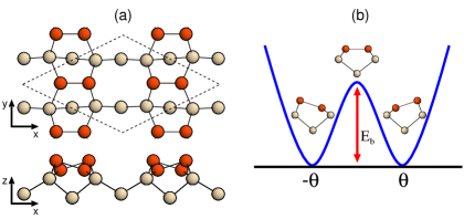
We begin to optimize both the symmetric dimer structure, forming a (21) periodicity (hereafter, designated as the (21) structure), and the (42) structure by using the DFT calculation within the generalized-gradient approximation (GGA) method . The optimized (42) structure is displayed in Fig. 1(a). We find that the (42) structure consisting of alternatively buckled dimers along and perpendicular to the dimer rows has a dimer bond length of = 2.357 Å and a dimer buckling angle of = 18.0∘. This (42) structure is found to be more stable than the symmetric-dimer structure by 255 meV per dimer, yielding = 255 meV [see Fig. 1(b)]. As shown in Fig. 2(a) and 2(b), the calculated band structure of (21) has a metallic band crossing the Fermi level , whereas that of (42) exhibits a semiconducting feature with a band gap of 0.27 eV. The present results for the geometry, energetics, and band structure of the (42) structure are in good agreement with those of previous DFT calculations Ram ; Sei .
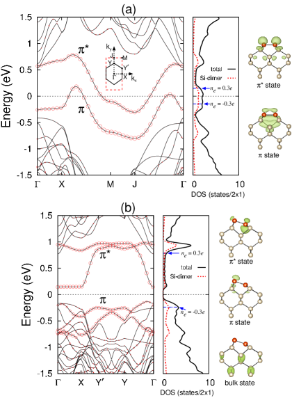
It has been known that below 40 K electrons or holes, injected through tunneling current in STM, result in surface charging due to a slow carrier relaxation between the surface layer and the semiconducting bulk Si Ono ; Bri ; Pol . In order to examine the influence of surface charging on the energetics of the (21) and (42) structures, we perform total-energy calculations for the two structures with electron or hole doping. For the simulation of surface charging, we use the virtual crystal approximation VCM to compensate excess electrons or holes (whose amount is represented as a negative value of ). Figure 3 shows the calculated values of as a function of ranging from 0.6 to 0.6 per (21) unit cell. We find that both the electron and hole dopings reduce the energy difference between the (21) and (42) structures. The resulting decrease of with electron or hole doping can be attributed to the metallic and semiconducting features of the (21) and (42) structures, respectively. As shown in Fig. 2(a) and 2(b), for instance of = 0.3, excess electrons in (21) are filled in the relatively lower unoccupied electronic states compared to those in (42), whereas holes in (21) are created in the relatively higher occupied electronic states compared to those in (42). Therefore, as electron (hole) doping increases, the total energy of the (21) [(42)] structure is expected to decrease (increase) more largely compared to the (42) [(21)] structure, leading to a decrease of .
As shown in Fig. 3, decreases more significantly with increasing hole doping, compared to the case of electron doping. This difference between electron and hole dopings may be due to the different characters of the unoccupied and occupied electronic states in the (42) structure: i.e., the lowest unoccupied states are mostly the surface states of orbitals, while the occupied states below consist of the surface states of orbitals as well as the bulk states [see the total density of states (DOS) and the local DOS of Si dimers in Fig. 2(b)]. We note that, for hole doping with = 0.3, the majority of the holes in the (42) structure is created in the bulk states around the point (see Fig. 1S of the Supplemental Material Supp ), possibly giving rise to a relatively larger strain energy compared to the (21) structure where holes are created mostly in the surface states. This fact may cause a more significant decrease of with hole doping, compared to electron doping where both the (42) and (21) structures occupy excess electrons mostly in their surface states.
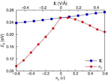
Next, we examine the influence of external electric field on the energetics of the (21) and (42) structures. Here, is simulated by superimposing an additional sawtooth potential along the [001] direction (taken as the + direction) with discontinuity at the mid-plane of the vacuum region of the supercell. Note that an STM bias voltage of 1.5 V and a tip-sample distance of 5 Å would give rise to an electrical field of 0.3 V/Å. Figure 3 also shows the calculated values of as a function of ranging between 0.5 and +0.5 V/Å. We find that increases (decreases) as increases along the + () direction. These different behaviors of depending on the direction of can be explained in terms of the different contributions of electrostatic energy due to external electric field between the (21) and (42) structures. Since the surface dipole moment pz (pointing direction) of the metallic (21) structure is larger in magnitude by 0.038 Å than that of the semiconducting (42) structure, an electric field applied along the + () direction gives a positively (negatively) larger electrostatic energy = of surface dipole in (21) compared to in (42), leading to an increase (decrease) of . We find that the variation of with respect to the external electric field of 0 0.5 V/Å is less than 20 meV, much smaller than that (160 meV) obtained from hole doping (see Fig. 3). Thus, we can say that the influence of hole doping on is much more pronounced than that arising from external electric field.
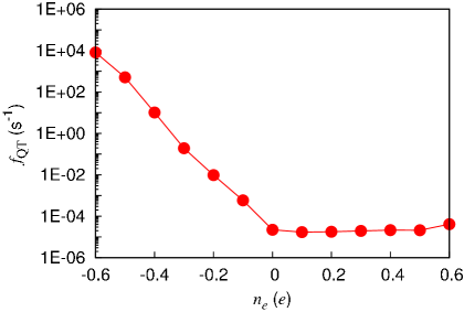
To account for the symmetric dimer images observed from low-temperature STM experiments Yokoyama1 ; Mitsui ; Ono ; Manzano , we investigate the flip-flop motion of buckled dimers driven by either thermal activation Hata2001 or quantum tunneling. For this, we assume a symmetric double-well potential [see Fig. 1(b)] that describes the potential energy surface of flipping dimers as a function of . Using a harmonic approximation, we obtain a vibration frequency for this potential well as = = 0.3 sec-1 in the absence of electron or hole doping, where the torsion constant and the inertia moment of flipping dimer can be estimated from = (: dimer buckling angle at the lowest-energy configuration) and = (: mass of Si atom). Based on an Arrhenius-type activation process, a thermally excited flipping rate can be expressed as = . With the calculated values of and as a function of 0.6, we obtain smaller than 0.8 sec-1 at 10 K. This thermal flipping rate is too small to explain the observed symmetric-dimer STM images with flicker noise Yokoyama1 ; Mitsui . As an alternative explanation for the flip-flop motion of buckled dimers, we consider quantum tunneling (QT) within the double-well potential, whose flipping rate can be approximated Fab ; Mer as
| (1) |
Contrasting with , is independent of temperature, while it is determined by the ratio of and the zero-point energy . The estimated values of are plotted as a function of . We find that sharply increases with increasing hole doping, while it is nearly flat with respect to electron doping. Here, note that electron doping decreases due to an increase of , thereby hardly changing the ratio of and . For hole doping with 0.3, becomes greater than 1.9 sec-1. Considering that it takes about 10-2 sec to obtain an STM image of a dimer, such a hole-doping induced flip-flop motion can produce the observed symmetric dimer images in low-temperature STM experiments Yokoyama1 ; Mitsui ; Ono ; Manzano . It is noticeable that the application of along the (+) direction decreases (increases) . Consequently, one expects that negative sample bias (equivalently, negative electric field) inducing hole doping at low temperature enhances the magnitude of . On the other hand, positive sample bias (positive electric field) inducing electron doping suppresses . These drastically different aspects of negative and positive bias voltages in low-temperature STM experiments account for the observations of symmetric and buckled dimer images in filled-state and empty-state images, respectively Ono ; Manzano .
Although we present a simple picture of the QT-driven flip-flop motion of buckled dimers with a double-well potential, we believe that it captures the microscopic mechanism underlying low-temperature symmetric-dimer STM images, as explained above. It is noted that the present DFT-GGA calculation may tend to somewhat overestimate the energy gain due to buckling. Indeed, the quantum Monte Carlo (QMC) calculation QMC which accurately describes electronic correlations extrapolates the value of up to 150 meV per dimer. Obviously, this reduction of should enhance the QT-driven flip-flop motion of buckled dimers. More rigorous QMC simulations with sufficiently large clusters or slab geometries will be a subject of future work.
In summary, we have performed a DFT-GGA calculation for the Si(001) surface to investigate the energy difference between the symmetric-dimer structure and the (42) structure under electron or hole doping as well as applied external electric field along the [001] direction. This energy difference corresponding to the energy barrier for the flipping of buckled dimers was found to decrease more significantly with respect to hole doping compared to electron doping. Consequently, we found that hole doping gives rise to a sizable QT-driven frequency of the flip-flop motion of buckled dimers while electron doping shows the marginal QT effects. These different QT aspects of hole and electron dopings are most likely to yield the imaging difference between the filled- and empty-state STM images at low temperature. Thus, we concluded that quantum tunneling enhanced by the tunneling-induced hole doping causes the observation of symmetric dimer images in low-temperature STM experiments.
ACKNOWLEDGEMENTS We thank Prof. Changgan Zeng, Prof. Shun-Fang Li, and Prof. Zhenyu Zhang for helpful discussions. This work was supported by the National Basic Research Program of China (Grant No. 2012CB921300), National Natural Science Foundation of China (Grants No. 11274280 and No. 61434002), and National Research Foundation of Korea (Grant No. 2015R1A2A2A01003248). The calculations were performed by KISTI supercomputing center through the strategic support program (KSC-2015-C3-017) for the supercomputing application research.
∗Corresponding author: chojh@hanyang.ac.kr
†Corresponding author: jiayu@zzu.edu.cn
References
- (1) J. Dabrowski and H.-J. Müssig, Silicon Surfaces and Formation of Interfaces (World Scientific, Singapore, 2000).
- (2) D. J. Chadi, Phys. Rev. Lett. 43, 43 (1979).
- (3) P.Krüger and J. Pollmann, Phys. Rev. Lett. 74, 1155 (1995).
- (4) J. T. Yates Jr., Science 279, 335 (1998).
- (5) G. Medeiros-Ribeiro, A. M. Bratkovski, T. I. Kamins, D. A. A. Ohlberg, and R. S. Williams, Science 279, 353 (1998).
- (6) R. A. Wolkow, Annu. Rev. Phys. Chem. 50, 413 (1999).
- (7) R. M. Tromp, R. J. Hamers, and J. E. Demuth, Phys. Rev. Lett. 55, 1303 (1985).
- (8) A. Ramstad, G. Brocks, and P. J. Kelly, Phys. Rev. B 51, 14504 (1995).
- (9) L. Kipp, D. K. Biegelsen, J. E. Northrup, L.-E. Swartz, and R. D. Bringans, Phys. Rev. Lett. 76, 2810 (1996).
- (10) T. Shirasawa, S. Mizuno, and H. Tochihara, Phys. Rev. Lett. 94, 195502 (2005).
- (11) R. A. Wolkow, Phys. Rev. Lett. 68, 2636 (1992).
- (12) Y. Kondo, T. Amakusa, M. Iwatsuki, H. Tokumoto, Surf. Sci. 453 L318 (2000).
- (13) T. Yokoyama and K. Takayanagi, Phys. Rev. B 61, R5078 (2000).
- (14) T. Mitsui and K. Takayanagi, Phys. Rev. B 62, R16251 (2000).
- (15) M. Ono, A. Kamoshida, N. Matsuura, E. Ishikawa, T. Eguchi, and Y. Hasegawa, Phys. Rev. B 67, 201306 (2003).
- (16) L. Perdigo, D. Deresmes, B. Grandidier, M. Dubois, C. Delerue, G. Allan, and D. Stivenard, Phys. Rev. Lett. 92, 216101 (2004).
- (17) K. Hata, S. Yoshida, and H. Shigekawa, Phys. Rev. Lett. 89, 286104 (2002).
- (18) C. Manzano, W. H. Soe, H. Kawai, M. Saeys, and C. Joachim, Phys. Rev. B 83, 201302(R) (2011).
- (19) I. Brihuega, O. Custance, M. M. Ugeda, N. Oyabu, S. Morita, and J. M. Gmez-Rodrguez, Phys. Rev. Lett. 95, 206102 (2005).
- (20) S. Polei, P. C. Snijders, S. C. Erwin, F. J. Himpsel, K.-H. Meiwes-Broer, and I. Barke, Phys. Rev. Lett. 111, 156801 (2013).
- (21) The present DFT calculations were performed using the FHI-aims code [V. Blum, R. Gehrke, F. Hanke, P. Havu, V. Havu, X. Ren, K. Reuter, and M. Scheffler, Comput. Phys. Commun. 180, 2175 (2009)] for an accurate, all-electron description based on numeric atom-centered orbitals, with “tight” computational settings. For the exchange-correlation energy, we employed the generalized gradient approximation of Perdew-Burke-Ernzerhof (PBE) [J. P. Perdew, K. Burke, and M. Ernzerhof,Phys. Rev. Lett. 77, 3865 (1996); 78, 1396(E) (1997)]. The Si(001) surafce (with the Si lattice constant = 5.418 Å) was modeled by a twelve-layer slab with 30 Å of vacuum in between the slabs, where each Si atom in the bottom layer was passivated by two H atoms. The -space integrations for the (21) and (42) structures were done equivalently with 32 points in the surface Brillouin zone of the (21) unit cell. Here, for the total-energy calculation of the (42) structure, we employed the equivalent (42) unit cell whose surface area is twice as large as that of the (42) structure. We used a dipole correction that cancels the artificial electric field across the slab [Neugebauer and Scheffler, Phys. Rev. B 272, 16067 (1992)]. All atoms except the bottom two layers were allowed to relax along the calculated forces until all the residual force components were less than 0.02 eV/Å.
- (22) K. Seino, W. G. Schmidt, and F. Bechstedt, Phys. Rev. Lett. 93, 036101 (2004)
- (23) For the simulation of surface charging, we used the virtual crystal approximation [Richter , Phys. Rev. Lett. 111, 045502 (2013)] to compensate excess electrons or holes, where the nuclear charge of Si atoms is modified by a small amount = / (: number of Si atoms within four deeper atomic layers).
- (24) See Supplemental Material at http://link.aps.org/supplemental/xx.xxxx/PhysRevLett.xxx.xxxxxx which includes the calculated surface band structure of the c(4 2) structure with a hole doping of = 0.3.
- (25) K. Hata, Y. Sainoo, and H. Shigekawa, Phys. Rev. Lett. 86, 3084 (2001).
- (26) F. Ronci, S. Colonna, and A. Cricenti, and G. Le Lay Phys. Rev. Lett. 99, 166103 (2007).
- (27) E. Merzbacher, Quantum Mechanics (J. Wiley, New York, 1970).
- (28) S. B. Healy, C. Filippi, P. Kratzer, E. Penev, and M. Scheffler, Phys. Rev. Lett. 87, 016105 (2001).