Titanium Nitride as a Seed Layer for Heusler Compounds
Abstract
Titanium nitride (\ceTiN) shows low resistivity at room temperature (), high thermal stability and thus has the potential to serve as seed layer in magnetic tunnel junctions. High quality \ceTiN thin films with regard to the crystallographic and electrical properties were grown and characterized by x-ray diffraction and 4-terminal transport measurements. Element specific x-ray absorption spectroscopy revealed pure \ceTiN inside the thin films. To investigate the influence of a \ceTiN seed layer on a ferro(i)magnetic bottom electrode in magnetic tunnel junctions, an out-of-plane magnetized \ceMn_2.45Ga as well as in- and out-of-plane magnetized \ceCo2FeAl thin films were deposited on a \ceTiN buffer, respectively. The magnetic properties were investigated using a superconducting quantum interference device (SQUID) and anomalous Hall effect (AHE) for \ceMn_2.45Ga. Magneto optical Kerr effect (MOKE) measurements were carried out to investigate the magnetic properties of \ceCo2FeAl. \ceTiN buffered \ceMn_2.45Ga thin films showed higher coercivity and squareness ratio compared to unbuffered samples. The Heusler compound \ceCo2FeAl showed already good crystallinity when grown at room temperature on a \ceTiN seed-layer.
I Introduction
Spintronic exploits the influence of the electron’s spin on its transport in solids. The key component of spintronic applications, like magnetic sensors or storage media, is the magnetic tunnel junction (MTJ). Spin dependent transport phenomena in MTJ’s, called tunnel magnetoresistance (TMR) effect, could be maximized for materials with high spin polarization. Thus half-metallic materials are preferred, due to a spin polarization of at the Fermi level. The half-metallic characteristic has been predicted for oxide compounds like \ceFe3O4 (Magnetite) and several Heusler compounds.Versluijs et al. (2001); Degroot et al. (1983) To achieve high crystalline ordering of the thin films, the lattice mismatch between the material and the substrate or seed layer has to be minimized. In addition a metallic buffer layer could act as a conduction layer. Common seed layers for Heusler compounds are \ceCr ( = ) and \cePt ( = ). Co-based Heusler compounds, like \ceCo2FeAl (\ceCFA), \ceCo2FeSi (\ceCFS), or \ceCo2MnSi (\ceCMS) have a lattice constant of . Therefore the use of a \ceCr buffer or \ceMgO substrate leads to epitaxial growth.Sterwerf et al. (2013) To maintain the thermal stability at shrinking device sizes, an out-of-plane oriented magnetization of the material is advantageous. Therefore perpendicularly magnetized \ceMn_3-xGa () compound found recently a lot of interest.
The perpendicular magnetocrystalline anisotropy (PMA) of the binary \ceMn-\ceGa compound is an intrinsic effect based on a crystal anisotropy. The spin polarization at the Fermi level of \ceMn-\ceGa is predicted to be for the tetragonally distorted phase.Balke et al. (2007) This crystalographic phase is formed if the mismatch between substrate and the thin film is small. In addition, the transition from the cubic into the tetragonal phase takes place at temperatures above 500.Glas et al. (2013a) To increase the applicability of these materials in magnetic tunnel junctions an optimized buffer layer is needed. \cePt is a promising material, due to the in-plane lattice constant of 3.92 Å and a lattice mismatch of 0.2 % to the in-plane lattice constant of the tetragonally distorted \ceMn-\ceGa (). Unfortunatly the favored growth direction of Pt on MgO (100) and \ceSrTiO3 (100) substrates is the (111) direction. Crystalline growth in the (001) direction is achieved by complicated preparation techniques. Furthermore \cePt is a critical raw material compared to Cr or Ti. For 45 degree rotated growth of the \ceMn-\ceGa the lattice mismatch with \ceCr is 5 %. Several groups reported crystalline \ceMn-\ceGa thin films on \ceCr buffered \ceMgO substrates. The diffusion temperature of Cr, however, is around 450, while \ceMn-\ceGa requires a deposition temperature of around 550. The diffusion problem also lowers the applicability of a Cr buffer for the Co-based Heusler compounds, like \ceCo2FeAl, Co2FeSi and Co2MnSi. To achieve high crystalline order of these compounds (L21 crystal structure) post-annealing processes have to be carried out at temperatures around . Investigations showed decreased TMR after the post annealing at such high temperatures, explained by \ceCr diffusion into the ferromagnetic electrode.Ebke et al. (2010); Sterwerf et al. (2013)
Due to the high thermal stability (melting point )Pritschow (2007) interdiffusion of \ceTiN is prevented. Another advantage is the low electrical resistivity of sputter deposited TiN () and a surface roughness below .Magnus et al. (2011); Krockenberger et al. (2012)
The lattice constant of \ceTiN (fcc structure) is and therefore suitable for various Heusler compounds. By rotating the unit cell of the Co-based Heusler compounds by 45 degree a lattice mismatch of about is achieved.
We investigated the structural properties of sputter deposited \ceTiN on single crystalline \ceMgO (001) and \ceSrTiO3 (001) substrates at different deposition temperatures using x-ray diffraction (XRD) and reflection (XRR). Since the surface properties are of large significancy for applications, atomic force microscopy (AFM) was carried out to verify the surface roughness. Temperature dependent transport measurements were realized in a closed cycled helium cryostat, with a temperature range from . X-ray absorption spectroscopy (XAS) was performed at beamline (BL) 6.3.1 of the Advanced Light Source in Berkeley. The Nitrogen -edge and Titanium -edges were investigated by surface sensitive total electron yield (TEY) and bulk sensitive luminescence mode (LM) in normal incidence. Furthermore, we investigated the crystallographic and magnetic properties of \ceCo2FeAl and \ceMn_3-xGa with \ceTiN seed layer deposited on \ceMgO and \ceSrTiO3 substrates.
II Experimental
DC and RF magnetron sputtering was used to prepare the samples. The \ceTiN as well as the \ceMn_2.45Ga layers were deposited in an UHV sputtering system with a base pressure below . Reactive sputtering in an Argon - Nitrogen atmosphere results in stoichiometric \ceTi1N1 thin films. During the sputtering a \ceN flow of combined with \ceAr was used, leading to a deposition pressure of . Because of the low lattice mismatch with \ceTiN (below ) \ceMgO (100) single crystalline substrates were used. \ceSrTiO3 (100) substrates were utilized, due to the low mismatch with the \ceMn-\ceGa crystal (below ). A \ceMn60Ga40 composite target and an Ar pressure of were used to deposit the \ceMn_2.45Ga thin films on top of the TiN. The deposition temperature of \ceTiN was , respectively. Whereas the \ceMn-\ceGa was deposited at . In addition \ceTiN buffered \ceCo2FeAl thin films on \ceMgO and \ceSrTiO3 substrates were prepared. For the \ceCo2FeAl, the substrates with a \ceTiN buffer layer were transfered to another magnetron sputtering machine, without vacuum break. Here the base pressure was . Stoichiometric \ceCo2FeAl was deposited from a composite target under an \ceAr pressure of . On top of the Heusler compound a thick \ceMgO layer was deposited to protect the stack from degradation.
III Results
III.1 Chrystallographic, structural and electrical properties of the TiN seed-layer
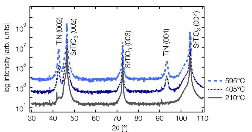
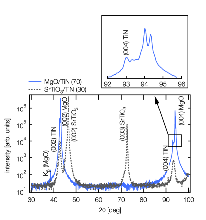
Crystallographic properties of the \ceTiN thin films () were determined using an X’Pert Pro diffractometer (\ceCu anode). The \ceTiN films showed no dependence of their crystalline quality on the deposition temperature on MgO substrates. Even at an epitaxial growth was obtained (not shown). On the contrary, \ceTiN layers on \ceSrTiO3 required a deposition temperature higher than to achieve epitaxial growth (Figure 1). Figure 2 shows an XRD pattern comparison of \ceTiN deposited on \ceMgO and \ceSrTiO3 substrate at . The thick \ceTiN film deposited on \ceMgO shows Laue oscillations, which are a clear evidence for high crystalline coherence (cutout in Figure 2). Due to the low lattice mismatch with \ceMgO the \ceTiN film reflexes are close to the substrate peaks and therefore difficult to investigate. The out-of-plane lattice constant, determined by the shoulder next to the (002) and (004) \ceMgO reflex, is Å. On \ceSrTiO3 substrates, the reflexes of the TiN layer are clearly visible and exhibit the same out-of-plane lattice constant.
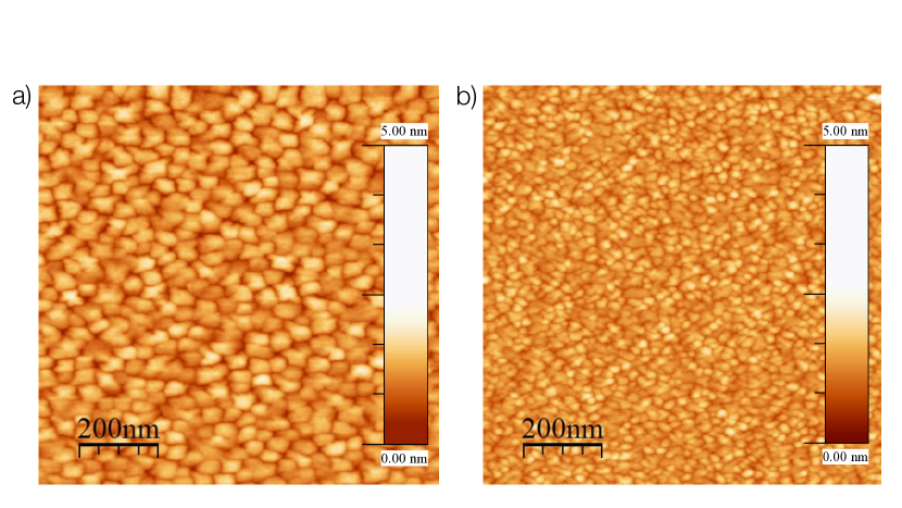
Atomic force microscopy and x-ray reflection measurements were carried out to investigate the surface roughness of the \ceTiN layers. The roughness obtained by XRR is between for all samples. The lowest value of was obtained for DC deposited \ceTiN with a deposition temperature of on both substrate types. AFM measurements of this samples (on a section) showed an RMS (root mean square) value of on \ceMgO (Figure 3 a) and on \ceSrTiO3 (Figure 3 b) substrate. The lower roughness values determined by AFM are attributed to the smaller scanned section compared to the XRR measurements. Another reason is that the AFM is only sensitive to the surface, so that possible gaps between the grains could not be detected. Whereas x-rays are penetrating into the sample surface and therefore are sensitive to steep grain boundaries. However, on \ceSrTiO3 both values are in good agreement, which was attributed to the smaller grain size of compared to on \ceMgO. Due to the reduced lateral grain size we obtain more grain boundaries on the scanned section, which leads to increased roughness.
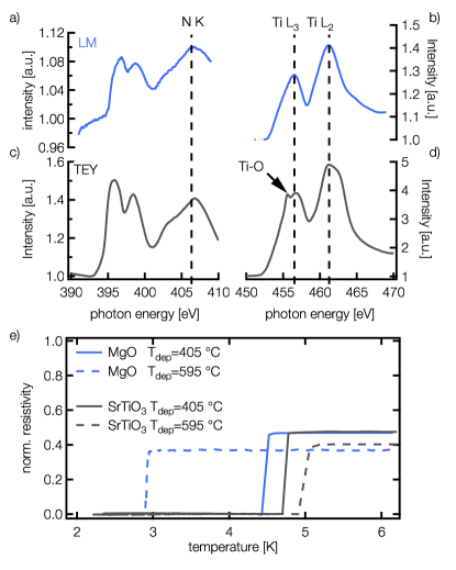
The chemical properties of \ceTiN thin films were investigated using XAS. Figure 4 a) - d) depicts the X-ray absorption spectra of \ceN and \ceTi taken in total electron yield TEY (grey) and luminescence mode LM (blue). The weak multiplet structure of the -\ceTi-edge indicates a small amount of \ceTi-\ceO on the surface. However, the bulk sensitive LM spectra of \ceTi and \ceN are in good agreement with the literature.Soriano et al. (1993)
| () | on \ceMgO (100) | on \ceSTO (100) |
|---|---|---|
| 405 | ||
| 595 |
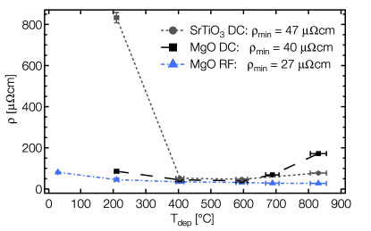
Temperature dependent transport measurements in a closed cycled \ceHe-cryostat revealed a transition into the superconducting state. The transition temperature showed a dependence on the substrate as well as on the deposition temperature of \ceTiN (Table 1 and Figure 4 e). The highest of was achieved for \ceTiN deposited at on \ceSrTiO3 substrate. However, the same stack on \ceMgO revealed the lowest of . Transport measurements at room temperature also showed a deposition temperature dependence of the resistivity (Figure 5). The lowest values of () for RF deposited \ceTiN on \ceMgO (DC deposited on \ceSrTiO3) was found for deposition temperatures of (). These data are in good agreement with the one reported by Shin et al.Shin et al. (2004) The high resistivity value of for \ceTiN deposited at (Figure 5) confirms the assumption that this temperature is too low to achieve crystalline growth of \ceTiN. The temperature and substrate dependence of the resistivity was attributed to the different grain sizes and film quality of \ceTiN obtained by different sputtering condicions. Due to the lower grain sizes on \ceSrTiO3 there are more grain boundaries inside the \ceTiN films and therefore more perturbations, which leads to a decreased conductance of the layer. Then again, this sample showed the highest transition temperature into the superconducting state, which is an evidence for high film quality with a low amount of impurities inside the layer. On the other hand, we obtained a reverse behavior for samples on \ceMgO. The low resistivity of the on \ceMgO substrates deposited thin films is attributed to bigger grains and high film quality of the \ceTiN compared to samples on \ceSrTiO3. In this case, increasing the deposition temperature leads to reduced . This reduction could be caused by oxygen impurities inside the \ceTiN.Münster and Sagel (1956) Increasing the deposition temperature causes a diffusion of oxygen atoms from the \ceMgO substrate into the \ceTiN layer leading to the formation of a \ceTi-\ceO interlayer between the substrate and the \ceTiN. \ceTi-\ceO is a semiconductor and therefore even a small amount inside the thin \ceTiN layer disturbes the transition into the superconducting state.
III.2 TiN buffered D022-Mn-Ga thin films
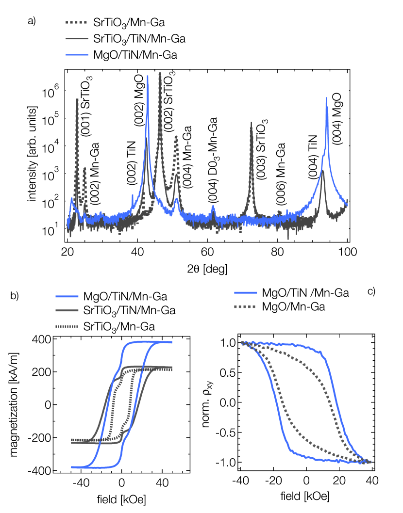
To investigate the suitability of \ceTiN as a seed layer, we deposited two different Heusler compounds on top of the \ceTiN. In a first attempt a perpendicularly magnetized \ceMn_Ga () thin film was deposited on a \ceTiN buffer layer on \ceMgO and \ceSrTiO3 substrates.
The \ceTiN seed-layer ( thickness) was DC sputter deposited at deposition temperatures of , respectively. The Mn-Ga was deposited at in order to achieve the tetragonally distorted D022 structure.Glas et al. (2013b) For all \ceTiN deposition temperatures the \ceMn-\ceGa shows two phases, a mixture of the tetragonal D022 structure with predicted out-of-plane magnetization and the cubic D03 phase with predicted in-plane magnetization (Figure 6 a). However, for \ceTiN deposited at a maximum amount of the D022 phase was observed. Furthermore, we added a \ceMn-\ceGa thin film on \ceSrTiO3 substrate without a \ceTiN buffer layer for comparison. The optimal deposition temperature to achieve the D022 structure of the \ceMn_Ga without a buffer layer was and therefore higher in contrast to \ceTiN buffered samples. All samples show the fundamental (004) D022-Mn-Ga reflex, corresponding to without \ceTiN buffer and with \ceTiN buffer. The lattice mismatch with the \ceTiN buffer leads to an expansion of the \ceMn-\ceGa unit cell along the - plane, which results in a lower lattice constant. Further to the fundamental D022 peak, the superlattice (002) reflex is visible for all samples. However, the superlattice (006) peak is only visible for \ceMn-\ceGa thin films without \ceTiN buffer. This indicates a lower amount and crystallinity of the tetragonally distorted D022 phase on \ceTiN buffered samples. The fundamental (004) peak of the D03 phase is weakly distinct, corresponding to on \ceSrTiO3 and on \ceMgO.
The magnetic properties of \ceMn-\ceGa were investigated using a superconducting quantum interference device. Figure 6 b) depicts the magnetization of \ceTiN buffered \ceMn-\ceGa thin films on \ceMgO (blue) and \ceSrTiO3 (grey). For comparison an unbuffered \ceMn-\ceGa thin film (grey dashed) is shown.
An overview of the coercivity c and the squareness of \ceTiN buffered \ceMn-\ceGa films on \ceMgO and \ceSrTiO3 is given in Table 2. We defined the squareness ratio by (0 kOe)/(60 kOe) for the SQUID measurements. \ceTiN buffered \ceMn_Ga shows increased coercivity and squareness on both substrate types. To prove this effect, additionally AHE measurements were carried out. Figure 6 c) shows normalized out-of-plane AHE hysteresis curves for \ceTiN buffered (blue) and unbuffered \ceMn-\ceGa layers (grey dashed). The c and values are given in Table 2. In this case we also observe an enhancement of the coercive field and squareness ratio for the \ceTiN buffered layer. The squareness ratio is defined by . It reveals a stronger enhancement compared to the sample on \ceSrTiO3 and increases from a value of to . \ceTiN buffered \ceMn-\ceGa thus requires lower deposition temperature compared to unbuffered samples to achieve an out-of-plane magnetization with high coercivity and squareness ratio. The saturation magnetization of on \ceMgO and on \ceSrTiO3 is in good agreement with the peviously reported results.Glas et al. (2013b) Interestingly, the saturation magnetization of the samples grown on \ceMgO, is twice as high as for the samples on \ceSrTiO3. This behavior was also observed for unbuffered samples and attributed to lower crystallinity due to bigger expansion in the - plane for \ceMn-\ceGa on \ceMgO substrates.Glas et al. (2013b) Obviously a \ceTiN layer does not change this behavior. Due to this expansion and therefore the imperfections in the crystal structure, the magnetic moments of the \ceMn atoms occupying the Wyckoff positons and are not compensating each other and this leads to an increase of the magnetization. The observed feature in the SQUID measurements around kOe field (Figure 6 b) is attributed to a second phase (soft magnetic) inside the \ceMn-\ceGa crystal structure, which has a different coercive field. The soft magnetic phase dominates at low field values and therefore leads to a sudden decrease or increase of the magnetization. A similar behavior was already observed for the ternary compounds \ceMn-\ceCo-\ceGa and \ceMn-\ceFe-\ceGa.Fowley et al. (2015); Gasi et al. (2013)
III.3 TiN buffered Co2FeAl thin films
| SQUID measurements | ||
| sample | (kOe) | |
| \ceSTO/ \ceMn_2.45Ga | ||
| \ceSTO/\ceTiN/\ceMn_2.45Ga | ||
| \ceMgO/\ceTiN/\ceMn_2.45Ga | ||
| AHE measurements | ||
| sample | (kOe) | |
| \ceMgO/\ceMn_2.45Ga | ||
| \ceMgO/\ceTiN/\ceMn_2.45Ga |
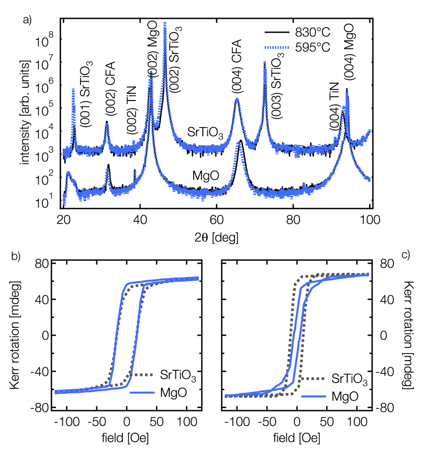
The influence of a TiN buffer layer on the magnetic and crystallographic properties of \ceCo2FeAl thin films was investigated in a second step. and thin \ceCo2FeAl layers were sputter deposited on a thick \ceTiN buffer on \ceMgO and \ceSrTiO3 substrates. The \ceTiN was DC sputter deposited at different temperatures (), whereas the \ceCo2FeAl deposition was carried out at room temperature. Figure 7 a) shows the obtained XRD spectra. Besides the characteristic \ceTiN reflexes, the fundamental and the superlattice peak of the \ceCo2FeAl are clearly visible. Even in the as deposited state, the XRD scan reveals a cubic structure with a (002) superlattice peak at 31.3 degree and a fundamental (004) reflex at 65.3 degree. Therefore a B2 order of the \ceCo2FeAl is proofed with an out-of-plane lattice constant of for \ceMgO substrates and for \ceSrTiO3 substrates. Interestingly, the lattice constant for samples on \ceSrTiO3 substrates is closer to the literature value of .Buschow et al. (1983) The \ceTiN deposition temperature does not influence the crystalline quality of the \ceCo2FeAl thin films.
In this case MOKE measurements were carried out to determine the magnetic properties. Figure 7 b) and c) illustrates the in-plane hysteresis loops for \ceTiN buffered thick \ceCo2FeAl films with a \ceTiN deposition temperature of . The \ceCo2FeAl films reveal sharp switching behavior and in-plane oriented easy magnetization axis, even in the as deposited state. The coercivity and squareness values of \ceCo2FeAl on \ceTiN are shown in Table 3. The squareness ratio is defined as Kerr rotation at Oe divided by Kerr rotation at Oe. The magnetic properties show a dependence on the substrate type as well as on the \ceTiN deposition temperature. With increasing \ceTiN deposition temperature, the coercive field decreases. In contrast the squareness ratio for samples on \ceSrTiO3 increases with increasing \ceTiN deposition temperature. As previously mentioned, different deposition temperatures affect the \ceTiN seed layer. The temperature during sputtering, and thus the surface energy has a strong influence on the crystal structure and grain size of the material. Structural changes of \ceTiN obviously influence the on top deposited material. Especially the grain sizes of the thin \ceCo2FeAl layers adjust to the grain structure of the seed layer. The coherence between grain size and coercivity of nanocrystalline ferromagnets was investigated by G. Herzer.Herzer (1990) He found a dependence of the coercivity for small grain sizes (up to ) and a dependence for bigger grains. In our case the grain size of \ceCo2FeAl is between . Therefore, the decrease of the coercive field of \ceCo2FeAl could be explained by a decrease of the grain sizes.
| substrate | (Oe) | ||
|---|---|---|---|
| \ceMgO | |||
| \ceSTO | |||
| \ceMgO | |||
| \ceSTO |
| (Oe) on \ceMgO | (Oe) on \ceSTO | |
|---|---|---|
Out-of-plane MOKE measurements for thin, TiN buffered, \ceCo2FeAl layers (Figure 8) revealed sharp switching (squareness ratio = ) and high thermal stability for both substrate types. Even for post annealing temperatures around strong perpendicular magnetic anisotropy and an increase of the coercivity was observed. The coercivity of the \ceCo2FeAl thin layers post annealed at is Oe on \ceMgO (blue curves) and Oe on \ceSrTiO3 (grey curves). Post annealing at leads to a Hc of Oe on \ceMgO and Oe on \ceSrTiO3. An overview is also given in Table 4. Compared to the results of Wen et al.Wen et al. (2011) for \cePt buffered \ceCo2FeAl thin films, where the PMA vanishes for post annealing temperatures of , the \ceTiN buffered \ceCo2FeAl layers provide high thermal stability, which in turn is beneficial for applications.
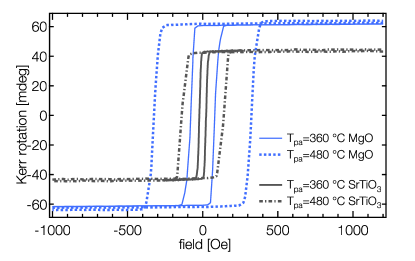
Additionally the \ceCo2FeAl shows a dependence of the coercivity on the used substrate. We also attribute this behavior to different grain sizes of \ceTiN on \ceMgO (\ceSrTiO3) substrates. As already shown in Figure 3 the grain size of \ceTiN on \ceMgO is twice as high () as on \ceSrTiO3 (). For the as deposited state we get a good agreement with a proportionality between coercivity and grain size. This behavior was explained theoretically by Alben et al. who found this proportionality for materials, where the induced anisotropy exceeds the structural anisotropy .Alben et al. (1978) In case of \ceCo2FeAl this is a necessary condition to obtain the perpendicular magnetocrystalline anisotropy, which we showed by the out-of-plane hysteresis curves. (Figure 8). A detailed discussion of the structural and magnetic properties of \ceTiN buffered \ceCo2FeAl thin films will be published elsewhere.
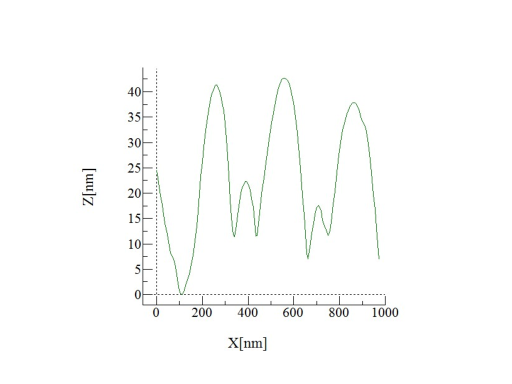
Investigations of the surface properties of the two compounds via AFM (Figure 9) revealed strong difference between the surface properties of \ceTiN buffered \ceMn_2.45Ga and \ceCo2FeAl. \ceMn_2.45Ga showed high roughness (RMS = ) and island growth ( grain size, determined using profiles of the AFM measurements (Figure 9), which is a strong drawback with regard to the applicability. However, \ceCo2FeAl thin films showed smooth surface (RMS = ), no island growth and small grains (). With regard to the integration of this layers into magnetic tunnel junctions, where low roughness plays an important role, \ceTiN buffered \ceCo2FeAl is a promissing candidate.
IV Conclusion
We successfully prepared (001) oriented \ceTiN thin films on \ceMgO and \ceSrTiO3 substrates. XAS measurements revealed the formation of pure \ceTiN in the thin films. A transition into the superconducting state was observed below . Transport measurements at room temperature showed a resistivity of on \ceMgO and \ceSrTiO3 substrates, respectively. It has been demonstrated that out-of-plane magnetized \ceMn_2.45Ga and \ceCo2FeAl thin films crystallize well on a \ceTiN seed layer. Even in the as deposited state \ceCo2FeAl provides the B2 crystal structure. \ceMn-\ceGa thin films exhibit higher coercivity and squareness ratio when prepared on a \ceTiN buffer. In addition a lower deposition temperature for \ceTiN buffered systems was observed. In-plane magnetized thick \ceCo2FeAl films revealed high squareness ratio even in the as prepared state. thin \ceCo2FeAl with out-of-plane oriented easy magnetization axis showed high thermal stability for temperatures up to . \ceTiN provides various advantages. The low resistivity makes \ceTiN a promising seed layer for Heusler compounds in MTJ’s. Besides the low roughness, high thermal stability and conductivity, it also enhances the out-of-plane magnetocrystalline anisotropy and optimizes the switching behavior of the used Heusler material. In case of \ceCo2FeAl, \ceTiN additionally enhances the thermal stability and therefore is highly preferable for applications.
Acknowledgments
The authors gratefully acknowledge financial support by the Deutsche Forschungsgemeinschaft (DFG, Contract No. RE 1052/32-1) and the opportunity to work at BL 6.3.1 of the Advanced Light Source, Berkeley, USA, which is supported by the Director, Office of Science, Office of Basic Energy Sciences, of the U.S. Department of Energy under Contract No. DE-AC02-05CH11231. D.E. is financially supported by the ERC Advanced Grant (291472 Idea Heusler).
References
- Versluijs et al. (2001) J. J. Versluijs, M. A. Bari, and J. Coey, Physical Review Letters 87, 026601 (2001).
- Degroot et al. (1983) R. Degroot, F. Mueller, P. Vanengen, and K. Buschow, Physical Review Letters 50, 2024 (1983).
- Sterwerf et al. (2013) C. Sterwerf, M. Meinert, J.-M. Schmalhorst, and G. Reiss, IEEE Transactions on Magnetics 49, 4386 (2013).
- Balke et al. (2007) B. Balke, G. H. Fecher, J. Winterlik, and C. Felser, Applied Physics Letters 90, 152504 (2007).
- Glas et al. (2013a) M. Glas, C. Sterwerf, J.-M. Schmalhorst, D. Ebke, C. Jenkins, E. Arenholz, and G. Reiss, Journal of Applied Physics 114, 183910 (2013a).
- Ebke et al. (2010) D. Ebke, P. Thomas, O. Schebaum, M. Schäfers, D. Nissen, V. Drewello, A. Hütten, and A. Thomas, Journal of Magnetism and Magnetic Materials 322, 996 (2010).
- Pritschow (2007) M. Pritschow, Ph.D. thesis, Institut für Mikroelektronik Stuttgart (2007).
- Magnus et al. (2011) F. Magnus, A. S. Ingason, S. Olafsson, and J. T. Gudmundsson, Thin Solid Films 520(5), 1621 (2011).
- Krockenberger et al. (2012) Y. Krockenberger, S.-i. Karimoto, H. Yamamoto, and K. Semba, Journal of Applied Physics 112, 083920 (2012).
- Soriano et al. (1993) L. Soriano, M. Abbate, H. Pen, M. T. Czyżyk, and J. C. Fuggle, Journal of electron spectroscopy and related phenomena 62, 197 (1993).
- Shin et al. (2004) C.-S. Shin, S. Rudenja, D. Gall, N. Hellgren, T.-Y. Lee, I. Petrov, and J. E. Greene, Journal of Applied Physics 95, 356 (2004).
- Münster and Sagel (1956) A. Münster and K. Sagel, Zeitschrift für Physik , 139 (1956).
- Glas et al. (2013b) M. Glas, D. Ebke, I. M. Imort, P. Thomas, and G. Reiss, Journal of Magnetism and Magnetic Materials 333, 134 (2013b).
- Fowley et al. (2015) C. Fowley, S. Ouardi, T. Kubota, O. Yildirim, A. Neudert, K. Lenz, V. Sluka, J. Lindner, J. M. Law, S. Mizukami, G. H. Fecher, C. Felser, and A. M. Deac, Journal of Physics D: Applied Physics 48, 164006 (2015).
- Gasi et al. (2013) T. Gasi, A. K. Nayak, J. Winterlik, V. Ksenofontov, P. Adler, M. Nicklas, and C. Felser, Applied Physics Letters 102, 202402 (2013).
- Buschow et al. (1983) K. Buschow, P. G. Van Engen, and R. Jongebreur, Journal of Magnetism and Magnetic Materials 38, 1 (1983).
- Herzer (1990) G. Herzer, IEEE Transactions on Magnetics 26, 1397 (1990).
- Wen et al. (2011) Z. Wen, H. Sukegawa, S. Mitani, and K. Inomata, Applied Physics Letters 98, 192505 (2011).
- Alben et al. (1978) R. Alben, J. Becker, and M. Chi, Journal of Applied Physics 49, 1653 (1978).