Modelling the intermixing effects in highly strained asymmetric InGaAs/GaAs quantum well
Abstract
In this work, we have theoretically investigated the intermixing effect in highly strained In0.3Ga0.7As/GaAs quantum well (QW) taking into consideration the composition profile change resulting from in-situ indium surface segregation. To study the impact of the segregation effects on the postgrowth intermixing, one dimensional steady state Schrodinger equation and Fick’s second law of diffusion have been numerically solved by using the finite difference methods. The impact of the In/Ga interdiffusion on the QW emission energy is considered for different In segregation coefficients. Our results show that the intermixed QW emission energy is strongly dependent on the segregation effects. The interdiffusion enhanced energy shift is found to be considerably reduced for higher segregation coefficients. This work adds a considerable insight into the understanding and modelling of the effects of interdiffusion in semiconductor nanostructures.
Key words: InGaAs/GaAs, quantum wells, modelling, interdiffusion, indium segregation, Fick’s law
PACS: 02.60.Cb, 02.70.Bf, 81.05.Ea, 81.07.St
Abstract
У данiй роботi ми теоретично дослiдили ефект взаємного перемiшування у сильнонапруженiй квантовiй ямi In0.3Ga0.7As/GaAs, беручи до уваги змiну концентрацiйного профiлю в результатi in-situ поверхневої сегрегацiї iндiю. З метою вивчення впливу ефектiв сегрегацiї на взаємне перемiшування в пiсляростовий перiод, чисельно розв’язанi одновимiрне рiвняння Шредiнгера в стацiонарному режимi i другий закон дифузiї Фiка, використовуючи методи скiнчених рiзниць. Розглянуто вплив взаємної дифузiї In/Ga на енергiю емiсiї квантової ями для рiзних коефiцiєнтiв сегрегацiї iндiю. Нашi результати показують, що енергiя емiсiї взаємноперемiшаних квантових ям сильно залежить вiд ефектiв сегрегацiї. Виявлено, що пiдсилений взаємною дифузiєю енергетичний зсув значно зменшується для вищих коефiцiєнтiв сегрегацiї. Ця робота значно поглиблює розумiння та моделювання ефектiв взаємної дифузiї у напiвпровiдникових наноструктурах.
Ключовi слова: InGaAs/GaAs, квантовi ями, моделювання, взаємна дифузiя, сегрегацiя iндiю, закон Фiка
1 Introduction
For the last decades, highly strained InGaAs/GaAs quantum wells (QWs) [1] have attracted considerable interest due to their fundamental physical properties and their potential capabilities for the fabrication of optoelectronic and photonic integrated circuits (PICs) [2, 3] high- power semi-conductor diode lasers [4, 5] and solar cells [6]. Due to its important role in adjusting the emission properties of quantum heterostructures, the interdiffusion process has been widely investigated theoretically and experimentally in various systems such as InGaAs/GaAs QW [7, 8, 9, 10, 11, 12, 13, 14] However, the interface broadening and distortion of In-concentration profiles result from the well-known indium surface segregation in InGaAs/GaAs QW during the growth process. This phenomenon leads to a significant deviation of the composition profiles from the expected rectangular shape of QWs [15]. This makes it difficult to accurately control the emission energy through the postgrowth intermixing process. That is why it is important to take into consideration this effect while modelling the QW electronic structure evolution as a function of the intermixing degree. Although In-segregation and In–Ga intermixing effects on InGaAs/GaAs heterostructure have been widely investigated as a separate phenomenon, less attention has been devoted to the investigation of the In-segregation impact on the intermixing process. In the present paper we theoretically investigate the intermixing effect for a strained InGaAs/GaAs QW taking into consideration the changes in the composition profile resulting from indium surface segregation during the growth process.
2 Theoretical considerations
During the growth of InGaAs layer on GaAs, a strong segregation of In atoms occurs which substantially alters the In distribution profile along the growth direction. Therefore, the quantum well optical and electronic properties are seriously changed by the segregation effects. This phenomena is mainly provoked by the high In mobility in the floating layer due to their small binding energy compared to that in the bulk material [16]. This effect has been quantified by Muraki et al. [13] in a phenomenological model, where a fraction of the deposited In atoms floats to the topmost surface and only the remaining portion will be incorporated. Accordingly, the In concentration in the -th layer is given by:
| (2.1) |
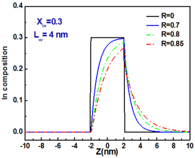
where is the segregation coefficient, is the nominal indium composition and is the number of InGaAs monolayers grown before depositing GaAs capping layer. Figure 1 shows the impact of the segregation coefficient on the In distribution profile of a 4 nm thick InGaAs QW with of In composition.
The asymmetrical In distribution profile complicates an accurate modelling of the emission energy dependence on the intermixing degree. Indeed, postgrowth intermixing process is highly required to voluntarily tune the QW emission energy for several applications. In this process, a thermally induced In/Ga atomic interdiffusion takes place leading to the modification of the In distribution profile and consequently alters the QW’s material band gap and the confined energy levels. It can be modelled by solving the conventional Fick’s second law of diffusion given by the equation (2.2) [17, 18]:
| (2.2) |
where presents the diffusivity, and it can be written as a function of the annealing temperature as follows:
| (2.3) |
where is the diffusion coefficient, is the activation energy for diffusion; is the Boltzmann constant, and respectively present the annealing temperature and the annealing time. The rate of indium concentration change is proportional to the concentration gradient . We assume that the diffusion coefficient is constant and all the atomic movement is independent of atomic concentration. The interdiffusion length is given as a function of the diffusivity and the annealing time by:
| (2.4) |
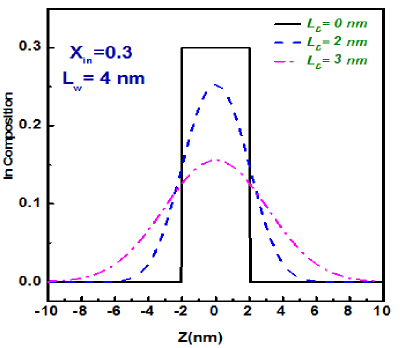
In most of the reported cases, where the segregation effect is neglected, an approximate solution based on the error function, given by the equation (2.5), is employed to model the QW intermixing at different diffusion lengths [20].
| (2.5) |
In this relation, represents the indium concentration at position , is the width of the InGaAs QW, is the indium mole fraction of the As-grown InGaAs layer and is the diffusion length. In the absence of segregation, a conventional rectangular QW has a symmetric In distribution profile. In this particular case , both equations (2.2) and (2.5) succeed in modelling the expected In distribution profile after postgrowth intermixing, as shown in figure 2, where the indium concentration profile is given for different diffusion lengths.
To evaluate the energy level and the emission energy for a strained In0.3Ga0.7As/GaAs QW and to study its dependence on the segregation and intermixing effects, the 1D stationary Schrödinger equation [21, 22] has been numerically solved:
| (2.6) |
where is the quantized energy level , ) and are, respectively, the wave function, the barrier potential energy, and the position dependent carrier’s effective mass in the growth direction is chosen to be along the axis. The numerical solution has been performed using the finite difference method within the framework of the effective mass approximation. The unstrained band gap energy InxGa1-xAs is given by the following formula:
| (2.7) |
where and are the unstrained band gap of InAs and GaAs materials and is the bowing parameter. The considered thickness and composition of the InGaAs material is below the critical thickness regime. Therefore, it can be considered as coherently strained. The mismatch between InxGa1-xAs and GaAs along the growth direction (-axis) result in a compressive strain leading to an increase in the band gap energy of the QW [18]. The uniaxial strain lifts the degeneracy of the light and heavy hole sub-bands at the centre of the brillouin zone [17]. The contribution of the hydrostatic strain to the bulk material’s band gap is given by:
| (2.8) |
and the change to the band gap due to the uniaxial component of the strain is given by:
| (2.9) |
where and are, respectively, the hydrostatic deformation potential and shear deformation potential, and are the stiffness constants, and the initial strain defined as:
| (2.10) |
and are, respectively, the lattice parameter of GaAs and InxGa1-xAs. All the parameters of the InxGa1-xAs material are deduced from those of GaAs and InAs materials by using Vegard’s law ensuring that their values depend on the In compositional profile [18]. The strained band gap is given by [20]
| (2.11) |
The confining potential for electrons in the conduction band and for holes in the valence band is equal to band gap discontinuity in each band.
| (2.12) |
where is the band offset taken to be for the conduction band and for the valence band.
3 Results and discussion
To achieve an accurate modelling of interdiffusion effect in InGaAs/GaAs QW, it is necessary to solve the exact Fick’s law equation.
Accordingly, we have applied equation (2.2) for In0.3Ga0.7As/GaAs QW ( nm) taking into account the indium segregation with an intermixing time t of 30 s. The solution of the Fick’s law allows to investigate the effect of the intermixing process on the band structure profile as a function of annealing temperature for different segregation coefficients.
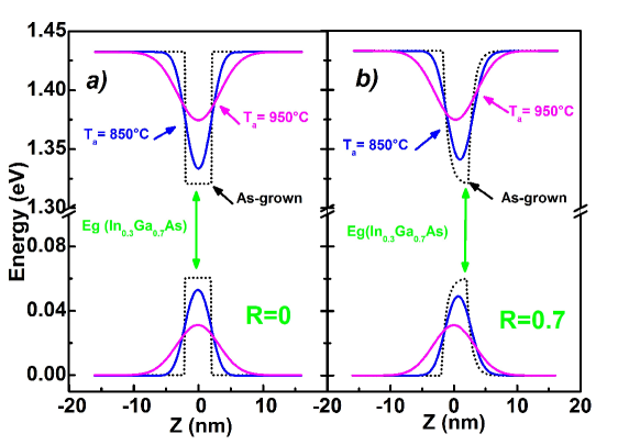
Figure 3 illustrates the typical intermixing effect of In0.3Ga0.7As QW at two annealing temperatures ℃, 950℃ for [figure 3 (a)] and [figure 3 (b)]. Under an annealing temperature of ℃, the band gap energy difference of InGaAs material arising from the segregation effects is found to be around 30 meV. In the meanwhile, for a higher intermixing degree, (℃), the InGaAs bandgap with segregation is only 10 meV higher than that of the reference QW (). The energy variation induced by the segregation effects is found to be reduced with an increase of the intermixing degree. This behavior is likely to arise from the overall decrease of the In concentration in the QW material [25]. This evolution also indicates that the intermixing induced energy shift may be strongly affected by the segregation phenomenon.
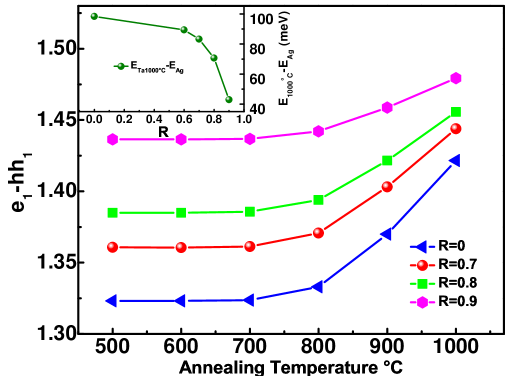
To illustrate this effect, we have calculated the evolution of the emission energy shift as a function of the annealing temperature for various values of the segregation coefficient , 0.7, 0.8, 0.9. The results are shown in figure 4, where the energy shifts are not significantly affected for ℃. However, for a higher annealing temperature, the results show an important energy shift. For example at ℃: it found to be about 100 meV for . However, it drops down to 45 meV for a larger segregation coefficient (). Indeed, the energy shift decreases as the segregation coefficient increases.
This evolution can be explained by an overall decrease in the indium composition and broadening in the InGaAs QW. As a result, the QW becomes poorer in indium and the interdiffusion effect becomes less sensitive to an increase of the annealing temperature. On the other hand, for high growth temperatures (℃), the segregation coefficient is generally accompanied by a decrease of the point defects’ density in the vicinity of the QW [19], thus enhancing the thermal stability of the QW structure which greatly reduces the phenomenon of interdiffusion.
4 Conclusion
In summary, we have theoretically investigated the interdiffusion effects in a single strained asymmetric InGaAs/GaAs QWs by numerically solving the Fick’s second law of diffusion and the one dimension Schrödinger equation. The calculations have been performed for QW with segregation effects and consequent asymmetric In distribution profile. The intermixing induced QW emission energy shift has been found to decrease with an increase of the segregation coefficient and interpreted in terms of overall reduction of In concentration. This work helps to improve the understanding of the intermixing effect in nanostructures.
Acknowledgement
The authors would like to extend their sincere appreciation to the Deanship of Scientific Research at king Saud University for its funding this Research group No. (RG–1436–014).
References
-
[1]
Sharma T.K., Jangir R., Porwal S., Kumar R., Ganguli T., Zorn M.,
Phys. Rev. B, 2009, 80, 165403;
doi:10.1103/PhysRevB.80.165403. -
[2]
Hatefi-Kargan N., Steenson D.P., Harrison P., Linfield E.H., Khanna S.,
Chakraborty S., Dean P., Upadhya P.C., Farrer I., Ritchie D.A., Sherliker B., Halsall M.,
Infrared Phys. Technol., 2007, 50, 106;
doi:10.1016/j.infrared.2006.10.024. - [3] Qiu Y.N., Sun H.D., Rorison J.M., Calvez S., Dawson M.D., Bryce A.C., Semicond. Sci. Technol., 2008, 23, 095010; doi:10.1088/0268-1242/23/9/095010.
- [4] Aimez V., Beauvais J., Beerens J., Ng. S.L., Ooi B., Appl. Phys. Lett., 2001, 79, 3582; doi:10.1063/1.1421234.
- [5] Paquette M., Aimez V., Bleauvais J., Beerens J., Poole J.P., Charbonneau S., Roth A.P., IEEE J. Sel. Top. Quantum Electron., 1998, 4, No. 4, 741; doi:10.1109/2944.720487.
- [6] Li X., Dasika V.D., Li P.-Ch., Ji L., Bank S.R., Yu E.T., Appl. Phys. Lett., 2014, 105, 123906; doi:10.1063/1.4896739.
- [7] Schiettekatte F., Aimez V., Chicoine M., Chevobbe S., Chabot J.F., Rajotte J.F., AIP Conf. Proc., 2003, 680, 609; doi:10.1063/1.1619790.
- [8] Chan M.C.Y., Surya C., Wai P.K.A., J. Appl. Phys., 2001, 90, 197; doi:10.1063/1.1370110.
- [9] Hulko O., Thompson D.A., Robinson B.J., Simmons J.G., J. Appl. Phys., 2009, 105, 073507; doi:10.1063/1.3103332.
- [10] Liu H.F., Liu W., Yong A.M., Zhang X.H., Chua S.J., Chi D.Z., J. Appl. Phys., 2011, 110, 063505; doi:10.1063/1.3638703.
- [11] Dixit V., Liu H.F., Xiang N., J. Phys. D: Appl. Phys., 2008, 41, 115103; doi:10.1088/0022-3727/41/11/115103.
-
[12]
Ghouma M., Hassen F., Sghaier H., Maaref H., Murray R.,
Microelectron. Eng., 1998, 43-44, 197;
doi:10.1016/S0167-9317(98)00164-6. - [13] Muraki K., Fukatsu S., Shiraki Y., Ito R., Appl. Phys. Lett., 1992, 61, 557; doi:10.1063/1.107835.
- [14] Yamaguchi K., Yasuda Y., Kovacs A., BarnavP.B., J. Appl. Phys., 2001, 89, 1; doi:10.1063/1.1331334.
- [15] Ilahi B., Sfaxi L., Bouzaiene L., Hassen F., Maaref H., Physica E, 2003, 17, 232; doi:10.1016/S1386-9477(02)00771-3.
-
[16]
Evans K.R., Kaspi R., Ehret J.E., Skowronski M., Jones C.R.,
J. Vac. Sci. Technol. B, 1995, 13, 1820;
doi:10.1116/1.587819. - [17] Chuang S.L., Physics of Optoelectronic Devices, Wiley, New York, 1995.
- [18] Vurgaftman I., Meyer J.R., Ram-Mohan L.R., J. Appl. Phys., 2001, 89, 5815; doi:10.1063/1.1368156.
-
[19]
Aziz Aghchegala V.L., Mughnetsyan V.N., Kirakosyan A.A.,
Superlattices Microstruct., 2011, 49, 99;
doi:10.1016/j.spmi.2010.11.008. - [20] Tsang J.S., Lee C.P.S., Lee H., Tsai K.L., Tsai C.M., Fan J.C., J. Appl. Phys., 1996, 79, 664; doi:10.1063/1.360810.
- [21] Ju G.-X., Cai C.-Y., Xiang Y., Ren Z.-Z., Commun. Theor. Phys., 2007, 47, 1001; doi:10.1088/0253-6102/47/6/007.
- [22] Zhanga A.-P., Shi P., Ling Y.-W., Hua Z.-W., Acta Phys. Pol. A, 2011, 120, 987.
-
[23]
Qu Y., Liu C.Y., Yuan S., Wang S.Z., Yoon S.F., Chan C.Y., Hong M.H.,
J. Appl. Phys., 2004, 95, 3422;
doi:10.1063/1.1651322. - [24] Charbonneau S., Poole P.L., Piva P.G., Aers G.C., Kotles E.S., Fallahi M., He J.-J., Mccaffery J.P., Buchanan M., Dion M., Goldberg R.D., Mitchell I.V., J. Appl. Phys., 1995, 78, 3697; doi:10.1063/1.359948.
-
[25]
Prol M., Moredo-Araujo A., Fraile-Pelaez F.J., Gomez-Alcala R., Superlattices Microstruct., 2001, 30, 2;
doi:10.1006/spmi.2001.0991.
Ukrainian \adddialect\l@ukrainian0 \l@ukrainian
Моделювання ефектiв взаємного перемiшування у сильнонапруженiй асиметричнiй InGaAs/GaAs квантовiй ямi
[]М. Соуаф, М. Байра, Г. Маареф, Б. Iлахi
Лабораторiя мiкроелектронiки i наноструктур, природничий факультет, Унiверситет Монастiр, Монастiр, Тунiс
Природничий коледж, унiверситет короля Сауда, Ер-Рiяд, Саудiвська Аравiя