Characterization of a gate-defined double quantum dot in a Si/SiGe nanomembrane
Abstract
We report the fabrication and characterization of a gate-defined double quantum dot formed in a Si/SiGe nanomembrane. In the past, all gate-defined quantum dots in Si/SiGe heterostructures were formed on top of strain-graded virtual substrates. The strain grading process necessarily introduces misfit dislocations into a heterostructure, and these defects introduce lateral strain inhomogeneities, mosaic tilt, and threading dislocations. The use of a SiGe nanomembrane as the virtual substrate enables the strain relaxation to be entirely elastic, eliminating the need for misfit dislocations. However, in this approach the formation of the heterostructure is more complicated, involving two separate epitaxial growth procedures separated by a wet-transfer process that results in a buried non-epitaxial interface 625 nm from the quantum dot. We demonstrate that in spite of this buried interface in close proximity to the device, a double quantum dot can be formed that is controllable enough to enable tuning of the inter-dot tunnel coupling, the identification of spin states, and the measurement of a singlet-to-triplet transition as a function of an applied magnetic field.
1 Introduction
Quantum dots in group-IV semiconductor heterostructures have the potential to be suitable for scalable quantum computing, and have made important steps in recent years towards that goal [1, 2]. Quantum dot qubits in silicon can be formed in several different ways by harnessing a combination of spin and/or charge states: successful realizations have demonstrated the single-spin qubit [3, 4, 5, 6], the singlet-triplet qubit [7, 8], the charge qubit [9, 10, 11], the exchange-only qubit [12], and the hybrid quantum dot qubit [13, 14]. While metal-oxide-semiconductor devices can confine electrons at the Si-oxide interface independent of the Si strain state, Si/SiGe heterostructures only confine electrons in the Si quantum well if that well is under tensile strain, a state that is typically achieved by epitaxial growth on relaxed SiGe [15]. Strain grading methods enable the growth of such relaxed SiGe buffer layers, allowing the confinement of electrons in a Si quantum well, and the formation of two-dimensional electron gases with very high mobility [16, 17].
However, the goal of making a large array of uniform Si/SiGe quantum dots is still a major challenge that must be overcome if they are to be used in a scalable quantum computer. A fault tolerant quantum computer may require as many as simultaneously tuned qubits [18], yet typical strain-graded heterostructures have qubit-affecting inhomogeneities on the length scale of a single qubit [19]. Three types of wafer inhomogeneities have been studied in detail: variation of lateral strain, mosaic structure, and disorder on Si/SiGe interfaces. Strain inhomogeneities will cause variation in the band gap offset [20], and strain-graded heterostructures have been shown to include 0.10% variations in strain over an area of 260 m2 [21]. Mosaic structure (i.e., tilting of crystalline lattice vectors) typically varies enough to impact spin qubits over length scales of one micron [19]. In addition, atomic level disorder on the interface between Si and SiGe layers, including single atomic steps, can greatly suppress the singlet-triplet splitting in quantum dots [22, 23].
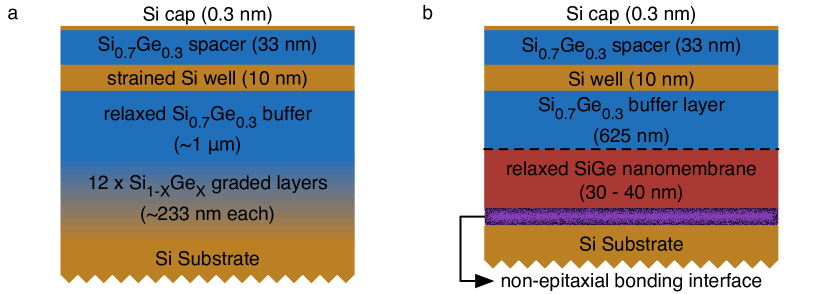
All three of these qubit-affecting defects are known to be caused by misfit dislocations, defects that are intentionally introduced as a part of the strain grading process [24]. A heterostructure formed through strain grading processes is depicted in Figure 1a. Regardless of how gradually strain is introduced into a heterostructure, strain grading processes will create a buried network of misfit dislocations [25]. As a consequence, one of the root causes of heterostructure inhomogeneities cannot be eliminated without adopting a new method of strain relaxation.
A liquid release method of elastic strain relaxation has been proposed as a path towards the production of highly uniform heterostructures, because it provides a path to the formation of relaxed SiGe without the introduction of misfit dislocations [26, 27, 21, 28]. The process begins by growing a layer of SiGe on silicon-on-insulator (SOI) such that its thickness is below the critical thickness necessary to form misfit dislocations. This single crystal SiGe nanomembrane is then released into liquid solution through subsequent HF, KOH, and H2O dips. Free of any rigid substrate, the nanomembrane elastically relaxes to its natural lattice constant. Finally, the nanomembrane is transferred to a new Si handle wafer where it can undergo further epitaxial growth to form the rest of the heterostructure. Figure 1b depicts a heterostructure created using the liquid release method of strain relaxation. Micro-Raman spectroscopy has shown that there is less lateral strain variation in such transferred nanomembrane heterostructures than in conventionally-strain-graded heterostructures [21]. Previous work has shown that electron gases formed in transferred nanomembranes have electron mobility above 40,000 cm2/(Vs) at a carrier density of 4 cm-2 [28], a mobility that in principle is high enough to form gate-defined quantum dots [29]. However, the nanomembrane transfer process necessarily introduces a non-epitaxial interface between the Si handle wafer and the transferred SiGe nanomembrane, and this interface has the potential to disrupt the tunability and stability of single-electron devices.
Here we report the first fabrication and characterization of a double quantum dot formed in a Si/SiGe nanomembrane heterostructure. We show that the nanomembrane heterostructure supports the formation and measurement of high-quality, gate-defined quantum dots, including the ability to reach the few electron regime, the ability to coherently tune the inter-dot tunnel coupling of two quantum dots, stability under the application of RF pulses, and sufficient repeatability to enable the performance of magnetospectroscopy of the quantum dot energy levels. These results provide strong evidence that the presence of a non-epitaxial interface between the silicon handle wafer and the wet-transferred nanomembrane does not degrade in an observable way the stability or performance of gate-defined quantum dots.
2 Methods
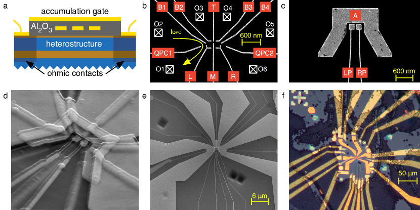
Figure 2a shows a schematic cross section of the Si/SiGe nanomembrane-based double quantum dot studied here, in which all carriers are induced by gates and no dopants are placed in the active area of the device [30, 31, 32, 33], eliminating a key source of charge noise [34]. After the second heterostructure growth on the elastically relaxed SiGe nanomembrane, a 10 nm layer of Al2O3 was grown by atomic layer deposition (ALD). To create ohmic contacts, regions of oxide were etched away, and at these locations 31P donors were implanted with a density of cm-2; these regions were subsequently covered with 4 nm Ti and 36 nm Au. The lower layer of gates was patterned using e-beam lithography and metallization with an e-beam evaporator (2 nm Ti/20 nm Au). Figure 2b shows a scanning electron microscope (SEM) image of a test pattern whose gate design is identical to the lower gate layer for the device studied here. This lower layer includes two quantum point contacts for charge sensing (QPC1,2), four barrier gates for controlling access to electron reservoirs (B1-4), left and right plunger gates outfitted for RF control of the dot (L and R), and a top (T) and middle gate (M) intended to control the inter-dot tunnel rate. A second layer of Al2O3 was grown using ALD, this time with a thickness of 80 nm, followed by an upper layer of accumulation gates, which was patterned and metallized with 2 nm Ti and 20 nm Au. Figure 2c shows a test pattern whose gate design is identical to the upper gate layer for the device studied here and includes a left and right paddle for changing dot occupation (PL and PR) and an accumulation gate to regulate access to the ohmic contacts (A). In a final lithography step, this accumulation gate was extended all the way to the ohmic contacts. Figure 2d is a tilt-view SEM image of the completed device.
Figure 2e is a larger-scale, top-down SEM image of the device and the surface of the surrounding heterostructure. Aside from a few pit defects, the heterostructure is quite uniform in the vicinity of the completed double quantum dot, demonstrating that membrane transfer is compatible with smooth and flat heterostructure regions. Figure 2f is an optical image at an even larger scale of the completed device; on this scale numerous tears and gaps are visible in the nanomembrane, and the device was carefully designed and fabricated to fit onto a clean and uniform portion of the nanomembrane. While this non-uniformity is present in the measured device and made the fabrication more challenging, it does not appear to be an inevitable part of nanomembrane devices; the damage observed in Figure 2f could have been avoided by carefully regulating the sonication power used during the cleaning step immediately prior to the second epitaxial growth. The completed double quantum dot structure was mounted in a dilution refrigerator with a base temperature of 40 mK.
3 Results and Discussion
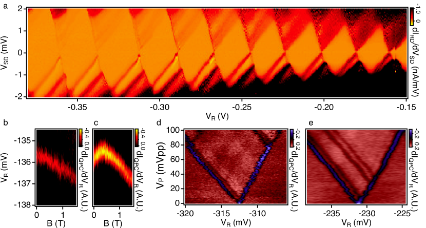
We first present measurements of a single quantum dot formed on the right side of the device (RD), which could be measured both by transport through the quantum dot between ohmic contacts O3 and O4 and by charge-sensing by measuring the current through the left quantum point contact, that is to say around QPC 1 and between ohmic contacts O1 and O2. Figure 3a shows the differential conductance across the quantum dot as a function of the applied source-drain bias voltage and the voltage on gate R. Numerous Coulomb diamonds are visible with no significant background charge rearrangement, demonstrating the stability of the background charge environment provided by the nanomembrane.
The Coulomb diamonds in Figure 3a increase in size with each expelled electron as gate voltage is made more negative, moving from right to left in the figure. Continuing in this direction, the quantum dot was brought into the few-electron regime by tuning the voltages on gates R and RP. Further characterization in the few-electron regime was performed by charge sensing using the left quantum point contact, performing a lock-in measurement of the current between ohmic contacts O1 and O2 while modulating . Figure 3b shows the results of magnetospectroscopy for a transition where the number of valence electrons changes from zero to one (below we show evidence that there may be an additional closed shell of electrons). As the in-plane magnetic field is increased from 0 T to 1.5 T, the transition from zero to one electron occurs at progressively lower values of , consistent with loading a spin-down electron. Figure 3c shows the results of an analogous magnetospectroscopy measurement on the 1-to-2 electron transition; in this case, as the applied magnetic field increases from 0 T to 0.38 T, the transition from one to two electrons occurs at progressively higher values of , consistent with a transition from a single spin-down electron to a two-electron singlet (S) state. In contrast, from T to 1.5 T the transition from one to two electrons occurs at progressively lower values of , consistent with the transition from a single spin-down electron to a two-electron triplet T- state. The transition of the two-electron ground state from singlet to triplet at T corresponds to a zero-field singlet-triplet splitting of 44 eV, comparable to values observed in quantum dots grown on conventional strain-graded heterostructures [37, 38, 7].
To probe the excited states of the dot, pulsed-gate spectroscopy was performed, with a square wave voltage applied to gate R enabling loading of excited states [39, 40]. The gate lever arms used to convert the voltage on gate R to the electrostatic energy of the right dot are eV/mV for the 0-to-1 electron transition and eV/mV for the 1-to-2 electron transition and were extracted from the slope of the transition lines in Figures 3b,c. Figure 3d shows data for the 0-to-1 transition; in this panel, a series of 420 ns square pulses with amplitude was applied to gate R with a repetition rate of 1 MHz. The single-electron excited state with the lowest energy is 56 eV above the ground state, an energy that is consistent with a predominately valley-like excitation in Si/SiGe quantum devices [23, 30, 41, 42]. In the upper left corner of Figure 3d a line extends towards the lower left and intersects with the so-called “loading line.” This line would correspond to an excited state of the 0-electron configuration, and thus it suggests the presence of a closed shell of electrons in the quantum dot. Figure 3e shows pulsed-gate spectroscopy for the 1-to-2 electron transition. For this transition, a series of 800 ns square pulses with amplitude was applied to gate R with a repetition rate of 500 kHz, which allowed loading of the two-electron excited states. Three two-electron excited states are visible; the two-electron excited state with the lowest energy sits 50 eV above the two-electron ground state, consistent with the singlet-triplet splitting observed in Figure 3c.
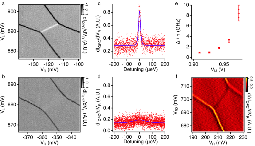
We now discuss the formation of a double quantum dot, for which gate M was used to control the inter-dot tunnel rate. Figures 4a,b show stability diagrams for the device, with Figure 4a acquired with V and Figure 4b acquired with V. The difference in tunnel rate between these two stability diagrams can be observed in two ways: first, while the polarization line in Figure 4a appears as a sharp, white line, the polarization line in Figure 4b is barely visible because the increased inter-dot tunnel rate leads to strong lifetime broadening. Second, whereas the dot-to-reservoir electron transitions in Figure 4a have sharp corners at their junction with the polarization line, the dot-to-reservoir electron transitions in Figure 4b show significant rounding near junctions with the polarization line.
To extract the tunnel coupling from Figure 4a, Figure 4c plots the lock-in signal as a function of the electrostatic energy difference between the left and right dots (the detuning), effectively superposing sections through the polarization line with many different values for the total double-dot energy. Each data point was projected onto the detuning axis using the pertinent gate lever arms; was established from the magnetospectroscopy data, and the other lever arms were determined geometrically from the slopes of the transition lines in Figure 4a and the value of . Following the approach of Ref. [36], we express , the current through the charge-sensing QPC, as
where is the detuning, is the energy difference between the two eigenstates, is the Boltzmann constant, is the electron temperature, is a current offset fit parameter, is a parameter for fitting the quantum point contact’s sensitivity to an inter-dot charge transition, and is a parameter characterizing gate-to-QPC crosstalk. The data from Figures 4c,d are fit with
where is the lever arm that converts changes in the voltage on gate R to changes in the detuning. The electron temperature T was taken to be 50 mK, consistent with the width of the dot-to-reservoir transitions (assumed to be primarily temperature broadened). The fits to the data in Figures 4c,d yield 0.970.08 GHz and 9.10.8 GHz, respectively, where is the inter-dot tunnel coupling. Figure 4e presents the results of a similar analysis for a total of 7 datasets, demonstrating the achievement of a wide range of tunnel couplings for various values of . The extraction of is difficult for very large tunnel couplings, as is clear from Figure 4d; for this reason, we plot two values of the tunnel coupling for V in Figure 4e, which were extracted from two different stability diagrams taken roughly a day and a half apart. Similarly, two values for the tunnel coupling are plotted for V, values which were extracted from separate stability diagrams taken roughly a day apart. In comparison to the data points for V, the two data points for V are in such close agreement that they are difficult to distinguish.
Finally, Figure 4f reports measurement of a double-dot stability diagram in the presence of short voltage pulses, demonstrating the stability of the device in the presence of very high-bandwidth driving. An arbitrary wave generator with a rise time of 40 ps was used to apply a series of 200 ps square pulses to gate L at a repetition rate of 20 MHz, which caused abrupt changes in the electric potential of the dots. When either dot was energetically close to a charge transition, applying such a series of pulses was likely to induce charge transitions in the dot, which caused a change in QPC current relative to a similar sequence of null pulses. Figure 4f shows the derivative of with respect to , which highlights regions where a charge transition is induced by the applied sequence of square pulses. The nanomembrane heterostructure of this device provides a stable electrostatic environment for the quantum dots, even when the double quantum dot system is driven by high-bandwidth voltage pulses.
4 Conclusions
The results discussed above demonstrate a new path towards the confinement of electrons in Si/SiGe gate-defined quantum dots: we have reported characterization of a double quantum dot formed in a heterostructure created using the liquid release method of strain relaxation. This method of strain relaxation is a powerful tool for the formation of heterostructures with much better uniformity than those created through conventional relaxation methods. The key advantage of this approach is that it does not depend on the insertion of misfit dislocations for strain relaxation, and instead it relies entirely on elastic relaxation of a single-crystal SiGe membrane. The measurements we report here address the stability of a double quantum dot fabricated on a Si/SiGe heterostructure grown epitaxially on such a transferred, relaxed SiGe nanomembrane. We demonstrated that the liquid release method of strain relaxation can produce quantum dots that are stable under a wide range of measurement conditions, and we showed that the inter-dot tunnel coupling was easily tuned over a wide range of values. The buried interface created during the wet transfer of the relaxed nanomembrane is far less controlled than the purely epitaxial heterostructures that in the past were used exclusively for Si/SiGe quantum dot experiments. The results presented above provide significant evidence that this interface formed 625 nm below the quantum well does not preclude the formation of high-quality and stable double quantum dots.
5 Acknowledgements
This work was supported in part by ARO (W911NF-12-0607), NSF (DMR-1206915, PHY-1104660), and the Department of Defense. The views and conclusions contained in this document are those of the authors and should not be interpreted as representing the official policies, either expressly or implied, of the US Government. Development and maintenance of the growth facilities used for fabricating samples is supported by DOE (DE-FG02-03ER46028). This research utilized NSF-supported shared facilities at the University of Wisconsin-Madison.
6 References
References
- [1] D. Loss and D. P. DiVincenzo. Quantum computation with quantum dots. Phys. Rev. A, 57(1):120–126, Jan 1998.
- [2] F. A. Zwanenburg, A. S. Dzurak, A. Morello, M. Y. Simmons, L. C. L. Hollenberg, G. Klimeck, S. Rogge, S. N. Coppersmith, and M. A. Eriksson. Silicon quantum electronics. Rev. Mod. Phys., 85:961, 2013.
- [3] E. Kawakami, P. Scarlino, D. R. Ward, F. R. Braakman, D. E. Savage, M. G. Lagally, M. Friesen, S. N. Coppersmith, M. A. Eriksson, and L. M. K. Vandersypen. Electrical control of a long-lived spin qubit in a Si/SiGe quantum dot. Nature Nanotech., 9:666–670, 2014.
- [4] M. Veldhorst, J. C. C. Hwang, C. H. Yang, A. W. Leenstra, B. de Ronde, J. P. Dehollain, J. T. Muhonen, F. E. Hudson, K. M. Itoh, A. Morello, and A. S. Dzurak. An addressable quantum dot qubit with fault-tolerant control-fidelity. Nature Nanotech., 9(12):981–985, 2014.
- [5] X. Hao, R. Ruskov, M. Xiao, C. Tahan, and H. W. Jiang. Electron spin resonance and spin–valley physics in a silicon double quantum dot. Nat. Comm., 5:3860, 2014.
- [6] M. Veldhorst, C. H. Yang, J. C. C. Hwang, W. Huang, J. P. Dehollain, J. T. Muhonen, S. Simmons, A. Laucht, F. E. Hudson, K. M. Itoh, A. Morello, and A. S. Dzurak. A two-qubit logic gate in silicon. Nature, 526:410, 2015.
- [7] B. M. Maune, M. G. Borselli, B. Huang, T. D. Ladd, P. W. Deelman, K. S. Holabird, A. A. Kiselev, I. Alvarado-Rodriguez, R. S. Ross, A. E. Schmitz, M. Sokolich, C. A. Watson, M. F. Gyure, and A. T. Hunter. Coherent singlet-triplet oscillations in a silicon-based double quantum dot. Nature, 481(7381):344–347, 2012.
- [8] Xian Wu, D. R. Ward, J. R. Prance, Dohun Kim, John King Gamble, R. T. Mohr, Zhan Shi, D. E. Savage, M. G. Lagally, Mark Friesen, S. N. Coppersmith, and M. A Eriksson. Two-axis control of singlet-triplet qubit with an integrated micromagnet. PNAS, 111:11938, 2014.
- [9] K. Wang, C. Payette, Y. Dovzhenko, P. W. Deelman, and J. R. Petta. Charge relaxation in a single-electron Si/SiGe double quantum dot. Phys. Rev. Lett., 111:046801, 2013.
- [10] Z. Shi, C. B. Simmons, D. R. Ward, J. R. Prance, T. S. Koh, J. K. Gamble, X. Wu, D. E. Savage, M. G. Lagally, M. Friesen, S. N. Coppersmith, and M. A. Eriksson. Coherent quantum oscillations and echo measurements of a Si charge qubit. Phys. Rev. B, 88(7):075416, 2013.
- [11] Dohun Kim, D. R. Ward, C. B. Simmons, John King Gamble, Robin Blume-Kohout, Erik Nielsen, D. E. Savage, M. G. Lagally, Mark Friesen, S. N. Coppersmith, and M. A. Eriksson. Microwave-driven coherent operations of a semiconductor quantum dot charge qubit. Nature Nanotechnol., 10:243–247, 2015.
- [12] Kevin Eng, Thaddeus D. Ladd, Aaron Smith, Matthew G. Borselli, Andrey A. Kiselev, Bryan H. Fong, Kevin S. Holabird, Thomas M. Hazard, Biqin Huang, Peter W. Deelman, Ivan Milosavljevic, Adele E. Schmitz, Richard S. Ross, Mark F. Gyure, and Andrew T. Hunter. Isotopically enhanced triple-quantum-dot qubit. Science Advances, 1(4), 2015.
- [13] Dohun Kim, Zhan Shi, C. B. Simmons, D. R. Ward, J. R. Prance, Teck Seng Koh, John King Gamble, D. E. Savage, M. G. Lagally, Mark Friesen, S. N. Coppersmith, and M. A. Eriksson. Quantum control and process tomography of a semiconductor quantum dot hybrid qubit. Nature, 511:70–74, 2014.
- [14] Dohun Kim, D. R. Ward, C. B. Simmons, D. E. Savage, M. G. Lagally, Mark Friesen, S. N. Coppersmith, and M. A. Eriksson. High fidelity resonant gating of a silicon based quantum dot hybrid qubit. preprint arXiv:1502.03156, 2015.
- [15] F. Schäffler. High-mobility Si and Ge structures. Semicond. Sci. Tech., 12(12):1515–1549, 1997.
- [16] K. Ismail, M. Arafa, K. L. Saenger, J. O. Chu, and B. S. Meyerson. Extremely high-electron-mobility in Si/SiGe modulation-doped heterostructures. Appl. Phys. Lett., 66(9):1077–1079, 1995.
- [17] T. M. Lu, D. C. Tsui, C.-H. Lee, and C. W. Liu. Observation of two-dimensional electron gas in a Si quantum well with mobility of 1.6106cm2/Vs. Applied Physics Letters, 94(18):182102, 2009.
- [18] Austin G. Fowler, Matteo Mariantoni, John M. Martinis, and Andrew N. Cleland. Surface codes: Towards practical large-scale quantum computation. Phys. Rev. A, 86:032324, 2012.
- [19] P. G. Evans, D. E. Savage, J. R. Prance, C. B. Simmons, M. G. Lagally, S. N. Coppersmith, M. A. Eriksson, and T. U. Schülli. Nanoscale distortions of Si quantum wells in Si/SiGe quantum-electronic heterostructures. Advanced Materials, 24(38):5217–5221, 2012.
- [20] Y. Sun, S. E. Thompson, and T. Nishida. Physics of strain effects in semiconductors and metal-oxide-semiconductor field-effect transistors. Journal of Applied Physics, 101(10), 2007.
- [21] D. M. Paskiewicz, D. E. Savage, M. V. Holt, P. G. Evans, and M. G. Lagally. Nanomembrane-based materials for group IV semiconductor quantum electronics. Scientific Reports, 4:4218, 2014.
- [22] M. Friesen, M. A. Eriksson, and S. N. Coppersmith. Magnetic field dependence of valley splitting in realistic Si/SiGe quantum wells. Appl. Phys. Lett., 89:202106, 2006.
- [23] S. Goswami, K. A. Slinker, M. Friesen, L. M. McGuire, J. L. Truitt, C. Tahan, L. J. Klein, J. O. Chu, P. M. Mooney, D. W. van der Weide, R. Joynt, S. N. Coppersmith, and M. A. Eriksson. Controllable valley splitting in silicon quantum devices. Nat. Phys., 3:41–45, 2007.
- [24] P. Mooney. Strain relaxation and dislocations in SiGe/Si structures. Materials Science and Engineering: R: Reports, pages 105–146, 1996.
- [25] P. M. Mooney, F. K. LeGoues, J. O. Chu, and S. F. Nelson. Strain relaxation and mosaic structure in relaxed SiGe layers. Applied Physics Letters, 62(26):3464–3466, 1993.
- [26] M. M. Roberts, L. J. Klein, D. E. Savage, K. A. Slinker, M. Friesen, G. Celler, M. A. Eriksson, and M. G. Lagally. Elastically relaxed free-standing strained-silicon nanomembranes. Nat Mater, 5:388–393, 2006.
- [27] Deborah M. Paskiewicz, Boy Tanto, Donald E. Savage, and Max G. Lagally. Defect-free single-crystal SiGe: A new material from nanomembrane strain engineering. ACS Nano, 5(7):5814–5822, 2011.
- [28] Y. S. Li, P. Sookchoo, X. Cui, R. Mohr, D. E. Savage, R. H. Foote, R. B. Jacobson, J. R. Sánchez-Pérez, D. M. Paskiewicz, S. Wu, D. R. Ward, S. N. Coppersmith, M. A. Eriksson, and M. G. Lagally. Electronic transport properties of epitaxial Si/SiGe heterostructures grown on single-crystal SiGe nanomembranes. ACS Nano, 9(5):4891–4899, 2015.
- [29] C. B. Simmons, M. Thalakulam, B. M. Rosemeyer, B. J. Van Bael, E. K. Sackmann, D. E. Savage, M. G. Lagally, R. Joynt, M. Friesen, S. N. Coppersmith, and M. A. Eriksson. Charge sensing and controllable tunnel coupling in a Si/SiGe double quantum dot. Nano Lett., 9:3234–3238, 2009.
- [30] M. G. Borselli, R. S. Ross, A. A. Kiselev, E. T. Croke, K. S. Holabird, P. W. Deelman, L. D. Warren, I. Alvarado-Rodriguez, I. Milosavljevic, F. C. Ku, W. S. Wong, A. E. Schmitz, M. Sokolich, M. F. Gyure, and A. T. Hunter. Measurement of valley splitting in high-symmetry Si/SiGe quantum dots. Appl. Phys. Lett., 98(12):123118, 2011.
- [31] D. R. Ward, D. E. Savage, M. G. Lagally, S. N. Coppersmith, and M. A. Eriksson. Integration of on-chip field-effect transistor switches with dopantless Si/SiGe quantum dots for high-throughput testing. Applied Physics Letters, 102:213107, 2013.
- [32] D. M. Zajac, T. M. Hazard, X. Mi, K. Wang, and J. R. Petta. A reconfigurable gate architecture for Si/SiGe quantum dots. Applied Physics Letters, 106:223507, 2015.
- [33] M. G. Borselli, K. Eng, R. S. Ross, T. M. Hazard, K. S. Holabird, B. Huang, A. A. Kiselev, P. W. Deelman, L. D. Warren, I. Milosavljevic, A. E. Schmitz, M. Sokolich, M. F. Gyure, and A. T. Hunter. Undoped accumulation-mode Si/SiGe quantum dots. Nanotechnology, 26:375202, 2015.
- [34] K. Takeda, T. Obata, Y. Fukuoka, W. M. Akhtar, J. Kamioka, T. Kodera, S. Oda, and S. Tarucha. Characterization and suppression of low-frequency noise in Si/SiGe quantum point contacts and quantum dots. Applied Physics Letters, 102:123113, 2013.
- [35] Hans Huebl, Christopher D. Nugroho, Andrea Morello, Christopher C. Escott, Mark A. Eriksson, Changyi Yang, David N. Jamieson, Robert G. Clark, and Andrew S. Dzurak. Electron tunnel rates in a donor-silicon single electron transistor hybrid. Phys Rev B, 81(23):235318, 2010.
- [36] L. DiCarlo, H. J. Lynch, A. C. Johnson, L. I. Childress, K. Crockett, and C. M. Marcus. Differential charge sensing and charge delocalization in a tunable double quantum dot. Phys. Rev. Lett., 92(22):226801, 2004.
- [37] Z. Shi, C. B. Simmons, J. R. Prance, John King Gamble, Mark Friesen, D. E. Savage, M. G. Lagally, S. N. Coppersmith, and M. A. Eriksson. Tunable singlet-triplet splitting in a few-electron Si/SiGe quantum dot. Appl. Phys. Lett., 99:233108, 2011.
- [38] J. R. Prance, Zhan Shi, C. B. Simmons, D. E. Savage, M. G. Lagally, L. R. Schreiber, L. M. K Vandersypen, Mark Friesen, Robert Joynt, S. N. Coppersmith, and M. A. Eriksson. Single-shot measurement of triplet-singlet relaxation in a Si/SiGe double quantum dot. Phys. Rev. Lett., 108:046808, 2012.
- [39] J. M. Elzerman, R. Hanson, L. H. Willems van Beveren, L. M. K. Vandersypen, and L. P. Kouwenhoven. Excited-state spectroscopy on a nearly closed quantum dot via charge detection. Appl. Phys. Lett., 84:4617–4619, 2004.
- [40] Madhu Thalakulam, C. B. Simmons, B. J. Van Bael, B. M. Rosemeyer, D. E. Savage, M. G. Lagally, Mark Friesen, S. N. Coppersmith, and M. A. Eriksson. Single-shot measurement and tunnel-rate spectroscopy of a Si/SiGe few-electron quantum dot. Physical Review B, 84(4):045307, 2011.
- [41] Zhan Shi, C. B. Simmons, Daniel R. Ward, J. R. Prance, Xian Wu, Teck Seng Koh, John King Gamble, D. E. Savage, M. G. Lagally, Mark Friesen, S. N. Coppersmith, and M. A. Eriksson. Fast coherent manipulation of three-electron states in a double quantum dot. Nature Comm., 5(3020):3020, 2014.
- [42] X. Mi, T. M. Hazard, C. Payette, K. Wang, D. M. Zajac, J. V. Cady, and J. R. Petta. Magnetotransport studies of mobility limiting mechanisms in undoped Si/SiGe heterostructures. Phys. Rev. B, 92:035304, 2015.