Quantum Transport Simulation of III-V TFETs with Reduced-Order Method
Abstract
III-V tunneling field-effect transistors (TFETs) offer great potentials in future low-power electronics application due to their steep subthreshold slope and large “on” current. Their 3D quantum transport study using non-equilibrium Green’s function method is computationally very intensive, in particular when combined with multiband approaches such as the eight-band method. To reduce the numerical cost, an efficient reduced-order method is developed in this article and applied to study homojunction InAs and heterojunction GaSb-InAs nanowire TFETs. Device performances are obtained for various channel widths, channel lengths, crystal orientations, doping densities, source pocket lengths, and strain conditions.
Keywords: III-V TFET; Heterojunction TFET; Source-pocket TFET; Strained TFET; method; Reduced-order method; Quantum transport.
1 Introduction
Scaling the supply voltage enables reduction of power consumption of integrated circuits. In order to continue reducing the supply voltage without degrading the performance, steep subthreshold swing (SS) transistors are highly needed. Steep tunneling field-effect transistors (TFETs) can achieve sub-60mV/dec SS at room temperature by using quantum-mechanical band-to-band tunneling (BTBT) ionescu2011tunnel ; seabaugh2010low . However, TFETs generally suffer from low “on” current () due to low tunneling probabilities. To enhance BTBT and increase , group III-V semiconductor based TFETs are very attractive since III-V materials can provide low band gap, small tunneling mass, and allow different band-edge alignments ionescu2011tunnel .
In order to achieve the best III-V TFET performances, it is required to systematically optimize various design parameters, such as the channel thickness, channel length, crystal orientations, doping densities, etc. In addition, many schemes have been proposed to further boost . The first scheme is to embed a pocket doping between the source and the channel nagavarapu2008tunnel ; jhaveri2011effect . The pocket increases the electric field near the tunnel junction and thus improves the and SS. 2-D quantum simulations has also been performed for this kind of device verreck2013quantum . The second scheme is to replace the homojunction with a heterojunction, for instance, a GaSb/InAs broken-gap heterojunction mohata2011demonstration ; dey2013high , or an InGaAs/InAs heterojunction zhao2014InGaAs . Due to the band offset between the two materials, the tunneling barrier height and distance are greatly reduced. 2-D and 3-D quantum transport simulations have also been performed for these heterojunction TFETs luisier2009performance ; jiang2013atomistic ; avci2013heterojunction . Other schemes include strain engineering conzatti2011simulation ; brocard2013design , grading of the molar fraction in the source region brocard2013design ; brocard2014large , adding a doped underlap layer between source and channel sharma2014GaSb , and embedding a quantum well in the source pala2015exploiting .
To understand the device physics, predict the performance, and optimize the design parameters of these structures, an efficient quantum transport solver is highly needed. The BTBT process can be accurately accounted for by combining non-equilibrium Green’s function (NEGF) approach datta2005quantum with tight binding or eight-band Hamiltonian. Unfortunately, these multi-band NEGF studies require huge computational resources due to the large Hamiltonian matrix. To improve their efficiency, equivalent but greatly reduced tight-binding models can be constructed for silicon nanowires (SiNWs) mil2012equivalent , which greatly speed up the simulation of p-type SiNW MOSFETs even in the presence of phonon scattering. Recently, this method has been extended to simulate III-V nanowire MOSFETs and heterojunction TFETs afzalian2015mode . Note that construction of the reduced tight binding models requires sophisticated optimization process. A mode space approach is also proposed for p-type SiNW MOSFETs and InAs TFETs shin2009full , which has been employed to simulate strain-engineered and heterojunction nanowire TFETs conzatti2011simulation ; brocard2013design . Though optimization process is not needed, this approach selects the modes only at the point, i.e., at , which is inefficient to expand the modes that are far away from .
In this work, we propose to construct the reduced-order models with multi-point expansion huang2013model ; huang2014model . We also extend this method to be able to simulate heterojunction devices. This efficient quantum transport solver is then applied to optimize device configurations such as crystal orientation, channel width, and channel length. Various performance boosters such as source pocket, heterojunction, and strain will be explored. Homojunction InAs and heterojunction GaSb/InAs nanowire TFETs will be the focus of this study.
The device structure is described in Section 2. The method is developed in Section 3, where the eight-band Hamiltonian and its matrix rotations are reviewed first. The rotated Hamiltonian is then discretized in a mixed real and spectral space. The accuracy of the method is benchmarked by comparing the band structures with tight binding method for several nanowire cross sections. The reduced-order NEGF method is developed in Section 4, where the reduced-order NEGF equations are summarized first. Then the problem of spurious bands, particular for the multi-point expansion, is identified. Afterwards, a simple procedure to eliminate these spurious bands is proposed. The method is finally validated by checking the band structures as well as the I-V curves. In Section 5, extensive simulations are carried out to understand and optimize the TFETs under different application requirements. Conclusions are drawn in Section 6.
2 Device Structure
The n-type gate-all-around (GAA) nanowire TFET to be simulated is illustrated in Fig. 1. The nanowire is P++ doped in the source and N+ doped in the drain, while it is intrinsic in the channel. A thin layer of N++ doping is inserted between the source and the channel to form a source pocket. The nanowire is surrounded by the oxide layer, through which the gate controls the channel (and the pocket).
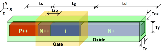
For homojunction TFETs in this study, all the source, pocket, channel, and drain are made of material InAs, because high “on” current is possible due to its small direct band gap and light effective masses luisier2009atomistic .
For heterojunction TFETs in this study, GaSb is used for the source while InAs is used for the pocket, channel and drain. These two materials form broken-gap heterojunction at the source-channel (or source-pocket) interface, though in reality staggered-gap heterojunction is formed due to lateral confinements luisier2009performance ; jiang2013atomistic .
Different channel width, gate length, and pocket length will be studied. The channel crystal orientations will be varied from [100] (with (010) and (001) surfaces), [110] (with (-1,1,0) and (001) surfaces), to [111] (with (-1,1,0) and (-1,-1,2) surfaces). The uniaxial stress will be applied along the direction while the biaxial stress will be applied in the and directions.
3 The Method
3.1 The Eight-Band Hamiltonian
To describe the band structure involving both the conduction and valence bands of III-V compound semiconductor materials, a widely used approach is the eight-band model. When the eight basis functions are chosen to be spin-up and spin-down and atomic orbital-like states, the zincblende Hamiltonian can be written as gershoni1993calculating ; enders1996exact ; wu2006impact ,
| (1) |
where the first part is spin-independent, the second part accounts for spin-orbit coupling, and the last part is deformation potential contribution due to strain.
With operator ordering (for heterostructures) taken into account, the four band Hamiltonian is
| (2) |
where and are the and identity matrices, and
| (3) |
| (4) |
| (5) |
| (6) |
Here the parameter is the conduction band edge with being the valence band edge and the band gap. is the valence band edge in the absence of spin-orbit coupling, with being the spin-orbit split-off energy. is proportional to the momentum matrix element and can be evaluated by its equivalent energy . is determined from the conduction band effective mass ,
| (7) |
The parameters , , and are related to the Luttinger parameters , , and ,
| (8) |
| (9) |
| (10) |
While the widely used symmetrized operator ordering evenly divides the terms leading to and , the correct Burt-Foreman ordering Foreman97 divides the terms according to different bands’ contribution, which leads to , , , and .
The spin-orbit terms and are
| (11) |
The strain Hamiltonian is Bahder90
| (12) |
where
| (13) |
| (14) |
Here is the strain vector in Voigt’s notation, is the deformation potential constant for the conduction band, , , , and , , are the Pikus-Bir deformation potential constants for the valence bands. Note that we only keep the independent terms.
The parameters for III-V compounds and their alloys can be found in Vurgaftman01 .
The Hamiltonian matrix defined in the above is in terms of in the crystal coordinate system (CCS). In practice, nanostructures can grow in different crystal directions, and thus the quantization directions and periodic directions are aligned with device coordinate system (DCS). Therefore it is more convenient to work in the DCS; and it requires coordinate transformation of the Hamiltonian matrix.
We first define a unitary rotation matrix from DCS to CCS , so that the vectors in the CCS and DCS, i.e., and , are related by
| (15) |
Note that the rows of are the coordinates of the CCS unit vectors in the DCS.
Then we rotate the matrix element by element. Each of the second order in terms in the CCS is of the form . Substituting (15), we have,
| (16) |
From above we can identify
| (17) |
Each of the first order in terms in the CCS is of the form , where is a matrix and is an matrix. Substituting (15), we have,
| (18) |
From above we can identify
| (19) |
and
| (20) |
The independent terms, such as the band edges and spin-orbit constants, do not need to rotate.
The strain and stress components are usually set in the DCS, however the strain components in the CCS are those that enter the Hamiltonian Esseni11 .
The rotation for the strain is given by
| (21) |
where and are the strain matrices in the CCS and DCS, respectively. Similar rotation holds for and , the stress matrices in the CCS and DCS.
It is convenient to transform directly the strain vector by
| (22) |
where and are the strain vectors in the CCS and DCS, respectively. is the transformation matrix, whose elements can be found by expanding equation (21). Similar rotation holds for and , the stress vectors in the CCS and DCS.
Finally, can be converted to via three elastic constants , , and ,
| (23) |
3.2 The Discretized Hamiltonian
For nanostructures, the periodicity is broken by the finite sizes and the external potentials. The eigen states can be found by solving the following coupled differential equation for envelop function (),
| (24) |
where is the slowly varying perturbed potential distribution, and operator is the element of with replaced by the differential operator .
In order to solve (24) numerically, the operator needs to be discretized first. To have a discretized form that is compact and valid for arbitrary nanowire orientation, we rewrite the eight-band operator (considering operator ordering) in (24) as,
| (25) |
where the matrices , , , and are the material- and orientation- dependent coefficients containing contributions from Löwdin’s renormalization, spin-orbit interaction, and strain.
In Ref. huang2013model , finite difference method (FDM) is adopted and it results in extremely sparse matrices. Therefore, the Bloch modes can be obtained efficiently with sparse matrix solvers. In fact, with shift-and-invert strategy implemented, the Krylov subspace based eigenvalue solver converges very quickly, as the eigenvalues of interest (close to the valence band top) distribute in a very small area. However, it is found that the Krylov subspace method is less efficient in the eight-band case. The reason is that the eigenvalues of interest distribute over a larger area, as both conduction and valence bands are to be sought and between them there is a band gap.
Therefore, the method used in Ref. shin2009full is employed, which is also generalized to arbitrary crystal orientations and to heterojunctions here. In this method, the transport direction is still discretized by FDM while the transverse directions are discretized by spectral method. Spectral method has high spectral accuracy (i.e., the error decreases exponentially with the increase of discretization points ) if the potential distribution is smooth paussa2010pseudospectral . This is true for devices that do not have any explicit impurities or surface roughness. So, the Hamiltonian matrix size of a layer, i.e., , can be kept very small (although it is less sparse or even dense), making direct solution of the eigenvalue problem possible.
To discretize the operator (25), the longitudinal component of the unknown envelope function is discretized with second-order central FDM,
| (26) |
| (27) |
| (28) |
where is the grid spacing.
The transversal components are expanded using Fourier series shin2009full , i.e.,
| (29) |
where and are the number of real space grid points in the and directions respectively, and are the coordinates of the th grid point in real space, and are the coordinates of the th grid point in the Fourier space,
| (30) |
where () is the nanowire thickness in the () direction. Note that hard wall boundary condition is enforced at the interfaces between the oxide layer and the semiconductor nanowire when the basis function (29) is used.
Operating (25) on (29), multiplying the result with (29) and performing integrations, we get the discretized form. It is block tridiagonal,
| (31) |
where is the on-site Hamiltonian for layer (), () is the coupling Hamiltonian between adjacent layers, and is the number of grids in the longitudinal direction .
The block of can be written down using very simple prescription,
| (32) | ||||
where and are the coordinates of the th and th grid points, respectively. is Kronecker delta function, for instance, is equal to 1 (0) if is an odd (even) number.
Similarly, the block of can be written as,
| (33) |
In this work, we use and have limited to be by employing the index scheme in shin2009full . This means 183 Fourier series are used to expand each wave function component, which is found to be sufficient. The dimension of is thus .
3.3 Comparison with TB Results
Since method is only valid in a small region around the point, there is a concern whether the method is accurate for small nanostructures. A comparison with full-band tight binding (TB) results will help answer this question. In order to have a fair comparison for confined structures, the parameters are fit to the bulk TB calculations. At first the bulk band structure is computed using the spin-orbit TB model, from which we have the band gap, spit-off energy, electron effective mass, heavy hole and light hole effective masses in both the [100] and [111] directions. These immediately determine parameters , , , , , and gershoni1993calculating ,
| (34) |
| (35) |
| (36) |
| (37) |
The remaining parameter is then slightly reduced from experiment value so as to avoid spurious solution veprek2007ellipticity . The fitted parameters for materials InAs and GaSb used in this work are list in Table 1, which slightly differ from those in Vurgaftman01 . The valence band offset (VBO) of GaSb relative to InAs is taken from Vurgaftman01 .
| Parameters | (eV) | (eV) | (eV) | VBO (eV) | ||||
| \svhline InAs | 0.368 | 0.381 | 0.024 | 19.20 | 8.226 | 9.033 | 18.1 | 0 |
| GaSb | 0.751 | 0.748 | 0.042 | 13.27 | 4.97 | 5.978 | 21.2 | 0.56 |
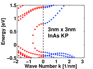
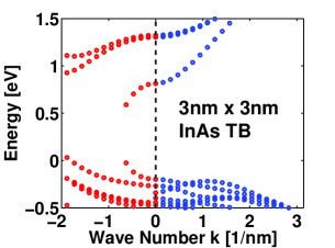
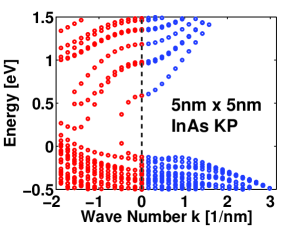
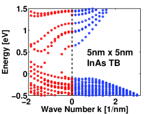
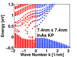
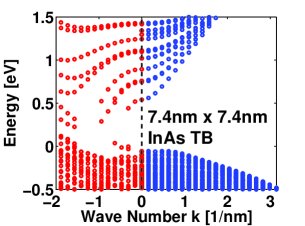
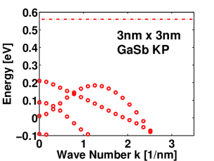
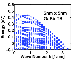
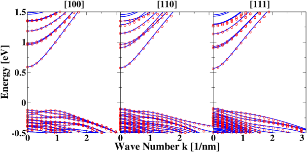
Fig. 2 compares the eight-band and spin-orbit TB band structures of three InAs nanowires with , , and cross sections, respectively. For , hard wall boundaries are imposed at the four surfaces while for TB the surface atoms are passivated with hydrogen atoms. Good matches are observed except for the case, where the model has larger separation of subbands though the band gaps are close.
The band edges and effective masses as functions of nanowire cross-section size are plotted in Fig. 3. The and TB results match quite well, except that band edges are slightly shifted downwards for small nanowires. These two models predict the same trends, i.e., as the nanowire size decreases both the band gap and the electron effective masses increase.
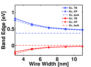
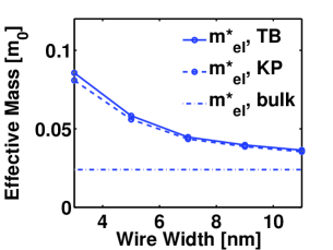
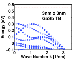
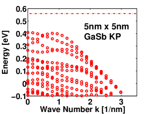
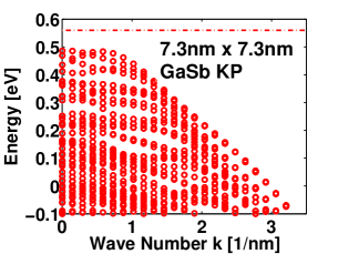
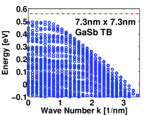
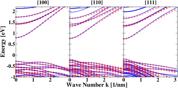
Fig. 4 compares and TB band structures of three GaSb nanowires with , , and cross sections, respectively. Only valence band is shown since it is the most relevant for transport in heterojunction GaSb/InAs TFET application here. Similar to InAs case, quantitative matches are observed except for the case where model predicts lower valence band edge and larger subband energies.
4 Reduced-Order NEGF Method
4.1 Reduced-Order NEGF Equations
The NEGF equations for the retarded and lesser Green’s function, and , in the mixed real and Fourier space can be written as,
| (38) |
| (39) |
where is the block three-diagonal Hamiltonian of the isolated device, is potential term that is block diagonal, and () is the retarded (lesser) self-energy matrix due to the semi-infinite leads, which is non-zero only in the first and last blocks. Phonon scattering has a very modest effect on the I-V curve conzatti2011simulation and coherent transport is sufficient for III-V homojunction and heterojunction TFETs with direct band gap luisier2010simulation ; Koswatta2010on , thus it is excluded in this work.
As the matrices involved are very large, to solve and efficiently for many different energy , the reduced-order matrix equations can be constructed,
| (40) |
| (41) |
and the reduced-order Green’s functions and are to be solved. Here, the reduced Hamiltonian, potential, self energy, and Green’s function are
| (42) |
where is a block-diagonal transformation matrix containing the reduced basis of each layer (with dimension , where is the number of reduced basis).
The gives the electron density. The hole density is obtained by subtracting electron density from the spectral function
| (43) |
In TFET, electrons can tunnel from valence band into conduction band and leave holes in the valence band. The charge density involving both electrons and holes is calculated by the method similar to Ref. guo2004toward .
| (44) | |||||
where is the layer dependent threshold (charge neutral level), which is taken as the mid band gap where is the average potential of layer . is the sign function. This model basically says that if a carrier is above (below) the threshold it is considered as an electron (hole). The required diagonal blocks of , i.e., , can be calculated with efficient recursive Green’s function (RGF) algorithm lake1997single , since the matrices are still block three-diagonal after the transformation.
The integrated is then transformed back into real space,
| (45) |
where is the transformation matrix from Fourier space to real space. Note that only diagonal terms are needed, which can be utilized to relieve the computational cost of back transformation. The transmission coefficient (and then ballistic current) can be calculated directly in the reduced space.
The problem now is how to construct this transformation matrix so that the reduced system is as small as possible, and yet it still accurately describes the original system. To construct the reduced basis for layer , the Hamiltonian of layer is repeated to form an infinite periodic nanowire. The reduction comes from the fact that only the electrons near the conduction band bottom and valence band top are important in the transport process. To approximate the band structure over that small region, then consists of the sampled Bloch modes with energy lying in that region. Multiple-point space sampling and (or) space sampling can be employed as has been demonstrated for the three- and six-band cases huang2013model . Here space sampling is adopted since space sampling is more costly and that the eight-band matrix is larger than the six- or three-band case.
4.2 Spurious Band Elimination
For three- and six-band models, as is shown in huang2013model , by sampling the Bloch modes at multiple points in the space and (or) space, a significantly reduced Hamiltonian can be constructed that describes very well the valence band top, based on which p-type SiNW FETs are simulated with good accuracy and efficiency. However, direct extension of this method to eight-band model fails. The problem is that the reduced model constructed by multi-point expansion generally leads to some spurious bands, a situation similar to constructing the equivalent tight binding models mil2012equivalent , rendering the reduced model useless.
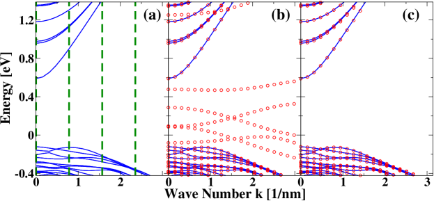
As an example, Fig. 5(a) plots the - dispersion for an ideal InAs nanowire orientated in the [100] direction. Fig. 5(b) is the result using the reduced Hamiltonian . The reduced basis ( is arbitrary here) is constructed by sampling the Bloch modes evenly in the Brillouin zone (at , , , and , as denoted in green lines in Fig. 5(a)), with the energy ( and are the confined valence and conduction band edges), which results in modes. Note that the modes at negative can be obtained by a transformation of those at positive huang2013model . Clearly, the reduced Hamiltonian reproduces quite well the exact dispersion in that energy window, demonstrating the number of sampling points is sufficient. However, there are also some spurious bands appearing in the conduction band and even in the band gap, making the reduced model useless. Moreover, different sampling points or sampling windows would change the number and position of the spurious bands. This situation is not encountered in the three- or six-band model involving only the valence bands, or in the one-band effective mass model involving the conduction band only. It should be caused by the coupling between the conduction and valence bands which makes the eight-band model indefinite. The coupling is important for materials with narrow band gaps.
The spurious bands must be suppressed. To this end, a singular value decomposition (SVD) is applied to the matrix . It is found that the singular values spread from a large value down to zero, indicating there are some linearly dependent modes. These linearly dependent modes give rise to null space of the reduced model and therefore must be removed. It is further found that the normal bands are mainly contributed by singular vectors having large singular values, in contrast to the spurious bands where singular vectors with small singular values also have large contribution. By removing the vectors with small singular values, i.e., vectors with where is the threshold, a new reduced basis is generated with . Using this new reduced basis, a new reduced Hamiltonian is constructed with its - diagram given in Fig. 5(c). It is observed that all the spurious bands have been eliminated at a cost of slightly compromised accuracy. The reduction ratio is , which is quite significant.
The value of is found to be crucial. A small might be insufficient to remove all the spurious bands while a large may degrade the accuracy severely. Moreover, adjustment of may be required when different sampling points or sampling energy windows are used. To determine automatically, we propose a search process as follows:
1. Sample enough Bloch modes and store them in matrix . Suppose points are sampled in the space, and modes with energy are obtained at the th point (), then the size of matrix is , where .
2. Do SVD of , i.e., .
3. Set an initial value for . Let us use here.
4. Use to construct a reduced basis by removing the singular vectors with in . The size of will be .
5. Use to build a reduced Hamiltonian . For each layer of , the size will be .
6. Solve the - relation of for certain , obtaining modes with . It is found that is a good choice.
7. If (which means that there are still some spurious bands), increase appropriately and go back to step 4. Otherwise, stop.
The above search process is fast, since step 5 and step 6 are much cheaper than step 1 although they have to be repeated many times. In fact, the complexity of step 1 is , step 2 is , step 5 is , and step 6 is . Note that .
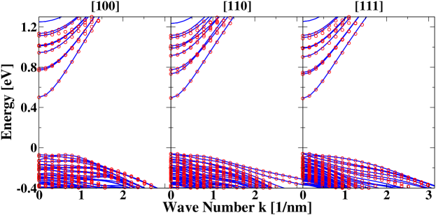
The used earlier is the result of the above search process. The above process also gives good results for nanowires in the [110] and [111] directions, as shown in Fig. 6. Different energy windows and are tested, again faithful results are obtained (not shown here). For other cross-section InAs nanowires such as the and in the [100], [110], and [111] orientations, this method gives reliable results, as shown in Fig. 7, and Fig. 8. It should be mentioned that this process results in a smaller basis set, which is different from the method for tight binding models mil2012equivalent where the basis is enlarged by putting in more modes to eliminate the spurious bands.
4.3 Error and Cost of the Reduced Models
Now this reduced model can be applied to simulate the TFET as shown in Fig. 1. Reduced NEGF equations and Poisson equation are solved self-consistently. To improve the efficiency, the reduced basis is constructed for an ideal nanowire with its potential term set to zero, so the reduced basis just needs to be solved only once for each material and it remains unchanged during the self-consistent iterations. The potential term in real devices then merely causes transitions between these scattering states. This assumption has been adopted in Ref. mil2012equivalent with good accuracy demonstrated. As will be shown below, it is also a fairly good approximation for the GAA nanowire TFET here.
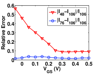
The - transfer characteristics of a cross section InAs homojunction TFET is plotted in Fig. 9(a). Three curves are compared. In the first, second, and third - curve, the valid energy window is , , and , respectively. The sampling k points are all at , , , and . This leads to , , and , with corresponding - curves denoted as , , and . Here can be considered as the reference, since with larger energy window and more modes the result is expected to have better accuracy. The relative errors of and relative to are calculated and plotted in Fig. 9(b). It is observed that has large deviations with respect to , especially when current is small. Instead is very close to and the relative errors are less than 4% for all bias points, indicating that the results have converged.
The - transfer characteristics of a cross section GaSb/InAs heterojunction TFET is plotted in Fig. 10(a). Burt-Foreman operator ordering is used at the material interface though symmetrized ordering gives similar results in this case. Due to the small lattice mismatch between GaSb and InAs, strain is small and is neglected here. Again, three I-V curves are compared. In the first, second, and third - curve, the energy window is , , and for GaSb, , , and for InAs. The sampling k points are all at , , , and . This leads to , , and for GaSb, , , and for InAs, with corresponding - curves denoted as , , and . The relative errors of and relative to are calculated and plotted in Fig. 10(b). It is observed that has very small deviations with respect to when above threshold current, but large errors when below threshold current. In contrast, has much better accuracy below threshold but larger error above threshold. Overall, the error of is still acceptable for predictive device modeling.
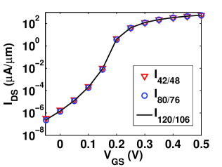
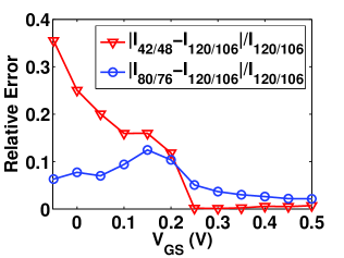
Table 2 lists the run time details for generating the above - curves. Note that homogeneous energy mesh with grid size is used which results in 359 energy points in total. Different energy points are calculated in parallel with 12 cores. All the simulations are performed on dual 8-core Intel Xeon-E5 CPUs. It is observed that the simulation time of one NEGF-Poisson iteration increases sub-linearly with ; different leads to small fluctuation of convergence (in terms of number of NEGF-Poisson iterations). In addition, the heterojunction TFET is harder to converge compared with homojunction case. Overall, the simulation time for one - curve took just a few hours, suitable for device design and optimization.
| - curves | ||||||
| \svhline One Iteration (minutes) | 2.38 | 2.96 | 4.09 | 2.47 | 3.02 | 4.21 |
| No. of Iterations | 41 | 47 | 43 | 87 | 82 | 98 |
| Total (minutes) | 97.6 | 139.1 | 175.9 | 214.9 | 247.7 | 412.6 |
5 Simulation Results
The above benchmarked quantum transport solver is used to study various device configurations as described in Section 2. Homojunction TFETs are simulated first with both n-type and p-type devices considered. Then various performance boosters are applied to the n-type devices, though the same ideas can be applied to p-type devices with qualitatively similar results expected. The device parameters are the same as those in Fig. 9 and Fig. 10 if not stated otherwise. In the following discussions, the current is normalized to the width of the nanowire to get unit of . We consider high performance (HP), low operating power (LOP), and low standby power (LSTP) applications, where the OFF currents are fixed to , , and , respectively.
5.1 Homojunction TFETs
Fig. 11 (a) compares the - curves with different gate lengths. It is found that the SS improves as gate length increases, while the turn-on characteristics remain unchanged. This is understandable since longer gate length has less source-to-drain tunneling leakage. As a result, improves when is fixed, as seen from Fig. 11 (b). The improvement is the largest for LSTP application and the smallest for the HP application. It is also found that will saturate when gate length becomes very long; the gate length at which saturates is shorter for HP application than for LSTP application. In the following simulations we fix the gate length to be 20nm.
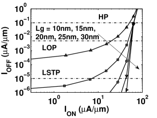
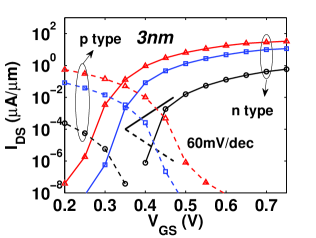
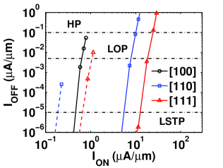
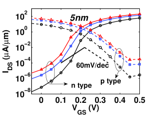
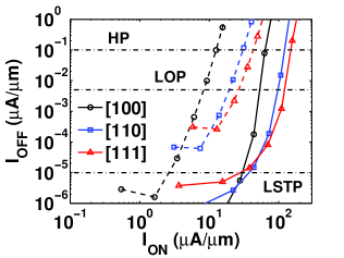
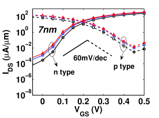
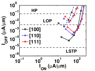
Fig. 12, 13, and 14 compare the - and - characteristics of InAs nanowire TFETs for three cross section sizes and for three transport directions. For p-type devices considered here, the doping density is set to at the source and at the drain, , . It is observed that, for small cross sections such as the 3nm case, although the SS are very small the are very limited, for all three orientations. This is due to their large electron effective masses and large band gaps. While for large cross sections such as the 7nm case, the SS degrades due to the smaller electron effective masses, smaller band gaps, as well as the weaker electrostatic control; the however are very good for both HP and LOP applications. It should be noted that are not sufficiently small which makes them unsuitable for LSTP application. The large are due to the direct source-to-drain tunneling leakage and ambipolar tunneling leakage at the channel-drain junction, these two components become more pronounced when band gap becomes smaller. Therefore, for LSTP application, medium sized cross section such as the 5nm case should be a better choice; otherwise, the channel length needs to be increased and/or the drain doping density needs to be decreased to suppress the leakage.
For small wire cross section, the performances of the three orientations differ a lot. In particular, for the 3nm case, [111] orientation gives the best for all three applications while [100] is the worst. When the cross section size increases, the three orientations tend to deliver similar performances. It also means that [111] orientation has the best cross-section scaling ability. In fact, when the confinement becomes stronger (as the nanowire size decreases) the band structure starts to differ from each other for the three orientations, as can be observed in Fig. 6, Fig. 7, and Fig. 8. In particular, the [100] orientation shows the fastest increase of band gap, while the [111] case shows the slowest increase of band gap meanwhile the hole effective mass decreases (as a result of strongly anisotropic heavy hole band).
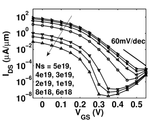
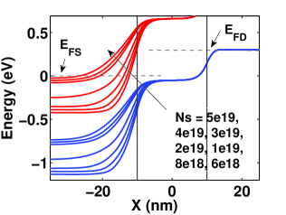
Comparing n-type and p-type devices, we found that p-type devices have worse SS and smaller . This is because the doping density has been set to at the source side, lower than that of n-type ones (which is ). This doping density is a compromise of SS and . In fact, as shown in Fig. 15, lower doping leads to smaller as a result of less abrupt tunneling junction. While higher doping leads to worse SS (approaching 60mV/dec) since larger Fermi degeneracy is created in the conduction band. The Fermi degeneracy creates thermal tail which counteracts the energy filtering functionality of TFETs. For 3nm (7nm) p-type TFETs here, smaller (larger) Fermi degeneracy in the source is observed because the electron mass and density of states increases (decreases) as cross section decreases (increases) (Fig. 3).
5.2 Improvements of Homojunction TFETs
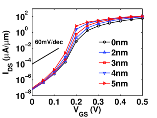
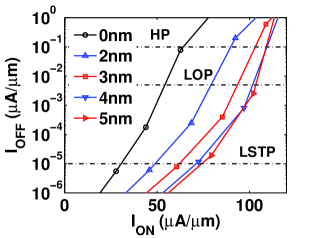
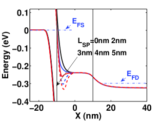
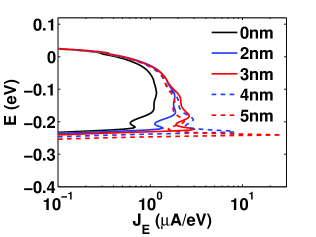
As shown in Fig. 16 (a) and (b), the source-pocket TFETs can improve for all HP, LOP, and LSTP applications, by up to . With 2nm to 5nm pocket lengths, first increases and then saturates. Further increasing the pocket length will decrease (not shown here). This can be explained by plotting the band diagram and current spectra, as shown in Fig. 16 (c) and (d). With 2nm to 5nm pocket lengths, the source pocket first increases the electric field across the source-channel tunneling junction and then starts to form a quantum well. This quantum well creates a resonant state leading to a very sharp tunneling peak. However, this peak is too narrow in energy to help the total current.
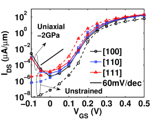
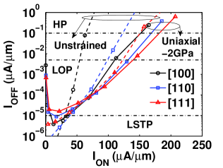
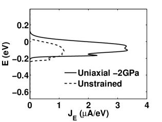
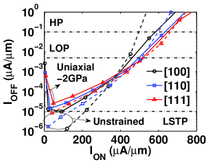
It has been shown in conzatti2011simulation that uniaxial compressive stress and biaxial tensile stress reduce InAs nanowire band gap and effective masses, which can be used to improve TFET performances. As shown in Fig. 17, the uniaxial compressive stress degrades the SS, but still improved is observed for both HP and LOP applications, consistent with conzatti2011simulation . The degraded SS can be explained by the large Fermi degeneracy of the source (due to lighter hole effective mass) creating thermal tail. It is found here that the strain induced improvement is more significant in the [100] orientation than in the [110] and [111] orientations, since the strain induced band gap and effective mass reductions are more pronounced in the [100] orientation. On the other hand, uniaxial tensile stress leads to increased band gap and effective masses and thus degraded (no shown here). Biaxial strain in the cross-section plane is hard to realize in experiments and therefore is not considered here.
5.3 Heterojunction TFETs
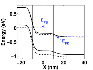
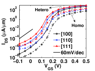
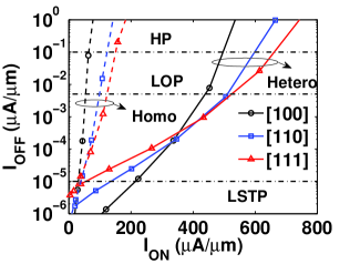
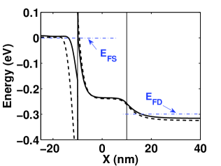
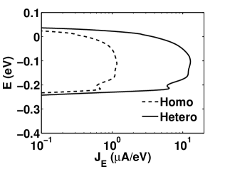
As shown in Fig. 18 (a) and (b), the GaSb/InAs heterojunction TFETs significantly improve for all HP, LOP, and LSTP applications. [111] orientation gives the best for both HP and LOP applications, while [100] gives the best for LSTP application. In Fig. 18 (c) and (d), we compare the band diagrams and current spectra of the GaSb/InAs heterojunction TFET with the InAs homojunction TFET. It is clear that the smaller tunneling height and distance of the heterojunction TFET, in particular at the GaSb side, leads to around larger tunneling current.
5.4 Improvements of Heterojunction TFETs
Employing the schemes for improving of homojunction TFETs, we get source-pocket heterojunction TFETs or strained heterojunction TFETs, which are expected to deliver even larger .
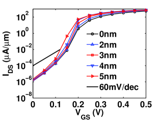
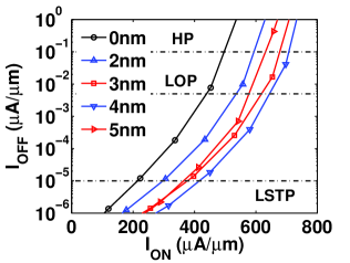
Indeed, as shown in Fig. 19 (a) and (b), the source pocket can improve for all HP, LOP, and LSTP applications, by up to . The optimal pocket length is found to be around 4nm, beyond which will drop. The physics is similar to the source-pocket homojunction TFETs and will not be repeated here.
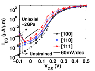
However, as shown in Fig. 20 (a) and (b), uniaxial compressive stress only slightly improves of [100] orientation for HP and LOP applications (and [110] orientation for HP application). In the [111] orientation, the stress even degrades . Again, uniaxial tensile stress leads to increased effective masses and thus degraded (no shown here). The physics is similar to the strained homojunction TFETs and will not be repeated here.
6 Conclusions
To efficiently simulate III-V nanowire based TFETs, a reduced-order NEGF method is developed. Through comparison with TB method, the method is shown to be able to describe quite well the band structures of very small nanowires. By introducing a spurious band elimination process, the reduced-order models can be constructed for reproducing the original band structures in an energy window near the band gap. The reduced models can also accurately capture the - characteristics of homojunction and heterojunction TFETs within a short simulation time.
InAs TFETs with different cross sections and channel orientations are compared, it is found that [111] direction has the best cross section scaling ability. Various performance boosters are studied. It is found that embedding source pockets can improve the “on” current due to the enhanced band bending at the source-to-channel junction, but this effect will saturate with increasing pocket length. Uniaxial compressive stress can also be used to boost the “on” current, which is found to be more effective in the [100] orientation than in the [110] and [111] orientations. Adopting GaSb/InAs heterojunction achieves a much larger “on” current due to the staggered-gap band alignment. Incorporating source pockets with proper pocket length into the heterojunction TFET is shown to further enhance the “on” current.
However, there is a large gap between theoretical projections and experiments lu2014tunnel . In experiments, the device performances are usually degraded by nonidealities such as phonon/dopant-induced band tails, defect-assisted tunneling, interface roughness and traps lu2014tunnel ; avci2015tunnel . To model these nonidealities, the Hamiltonian needs to be modified properly to account for these defects and the transport solver needs to be extended to incorporate various scattering events due to impurity, alloy, phonon, and surface roughness. These will be done in the future.
Acknowledgment
The use of nanoHUB.org computational resources operated by the Network for Computational Nanotechnology funded by the US National Science Foundation under Grant Nos. EEC-0228390, EEC-1227110, EEC-0228390, EEC-0634750, OCI-0438246, OCI-0832623 and OCI-0721680 is gratefully acknowledged.
References
- (1) A. M. Ionescu and H. Riel, “Tunnel field-effect transistors as energy-efficient electronic switches,” Nature, vol. 479, pp. 329–337, 2011.
- (2) A. C. Seabaugh and Q. Zhang, “Low-voltage tunnel transistors for beyond CMOS logic,” Proc. IEEE, vol. 98, no. 12, pp. 2095–2110, Dec. 2010.
- (3) V. Nagavarapu, R. Jhaveri, and J. C. Woo, “The tunnel source (pnpn) n-MOSFET: A novel high performance transistor,” IEEE Trans. Electron Devices, vol. 55, no. 4, pp. 1013–1019, 2008.
- (4) R. Jhaveri, V. Nagavarapu, and J. C. Woo, “Effect of pocket doping and annealing schemes on the source-pocket tunnel field-effect transistor,” IEEE Trans. Electron Devices, vol. 58, no. 1, pp. 80–86, 2011.
- (5) D. Verreck, A. Verhulst, K.-H. Kao, W. Vandenberghe, K. De Meyer, and G. Groeseneken, “Quantum mechanical performance predictions of p-n-i-n versus pocketed line tunnel field-effect transistors,” IEEE Trans. Electron Devices, vol. 60, no. 7, pp. 2128–2134, 2013.
- (6) D. K. Mohata, R. Bijesh, S. Mujumdar, C. Eaton, R. Engel-Herbert, T. Mayer, V. Narayanan, J. M. Fastenau, D. Loubychev, A. K. Liu, and S. Datta “Demonstration of MOSFET-like on-current performance in arsenide/antimonide tunnel FETs with staggered hetero-junctions for 300mV logic applications,” IEEE IEDM Tech. Dig., Dec. 2011, pp.33.5.1–33.5.4.
- (7) A. W. Dey, B. M. Borg, B. Ganjipour, M. Ek, K. A. Dick, E. Lind, C. Thelander, and L.-E. Wernersson, “High-current GaSb/InAs(Sb) nanowire tunnel field-effect transistors,” IEEE Electron Devices Lett., vol. 34, no. 2, pp. 211–213, 2013.
- (8) X. Zhao, A. Vardi, and J. A. del Alamo, “InGaAs/InAs heterojunction vertical nanowire tunnel FETs fabricated by a top-down approach,” IEEE IEDM Tech. Dig., Dec. 2014, pp.25.5.1–25.5.4.
- (9) M. Luisier and G. Klimeck, “Performance comparisons of tunneling field-effect transistors made of InSb, Carbon, and GaSb-InAs broken gap heterostructures,” IEEE IEDM Tech. Dig., Dec. 2009, pp. 1–4.
- (10) Z. Jiang, Y. He, G. Zhou, T. Kubis, H. G. Xing, and G. Klimeck, “Atomistic simulation on gate-recessed InAs/GaSb TFETs and performance benchmark,” DRC, Jun. 2013, pp. 145–146.
- (11) U. E. Avci and I. A. Young, “Heterojunction TFET scaling and resonant-TFET for steep subthreshold slope at sub-9nm gate-length,” IEEE IEDM Tech. Dig., Dec. 2013, pp.4.3.1–4.3.4.
- (12) F. Conzatti, M. G. Pala, D. Esseni, E. Bano, and L. Selmi, “Strain-induced performance improvements in InAs nanowire tunnel FETs,” IEEE Trans. Electron Devices, vol. 59, no. 8, pp. 2085–2092, 2012.
- (13) S. Brocard, M. G. Pala, and D. Esseni, “Design options for hetero-junction tunnel FETs with high on current and steep sub-threshold voltage slope,” IEEE IEDM Tech. Dig., Dec. 2013, pp.5.4.1–5.4.4.
- (14) S. Brocard, M. G. Pala, and D. Esseni, “Large on-current enhancement in hetero-junction tunnel-FETs via molar fraction grading,” IEEE Electron Devices Lett., vol. 35, no. 2, pp. 184–186, 2014.
- (15) A. Sharma, A. A. Goud, and K. Roy, “GaSb-InAs n-TFET with doped source underlap exhibiting low subthreshold swing at sub-10-nm gate-lengths,” IEEE Electron Devices Lett., vol. 35, no. 12, pp. 1221–1223, 2014.
- (16) M. G. Pala, and S. Brocard, “Exploiting hetero-junctions to improve the performance of III-V nanowire tunnel-FETs,” IEEE J. Electron Devices Soc., vol. 3, no. 3, pp. 115–121, 2015.
- (17) S. Datta, Quantum Transport: Atom to Transistor. Cambridge, U.K.: Cambridge Univ. Press, 2005.
- (18) M. Shin, “Full-quantum simulation of hole transport and band-to-band tunneling in nanowires using the method,” J. Appl. Phys., vol. 106, no. 5, pp. 054505-1 -054505-10, Sep. 2009.
- (19) G. Mil’nikov, N. Mori, and Y. Kamakura, “Equivalent transport models in atomistic quantum wires,” Phys. Rev. B, vol. 85, no. 3, pp. 035317-1 -035317-11, 2012.
- (20) A. Afzalian, J. Huang, H. Ilatikhameneh, J. Charles, D. Lemus, J. Bermeo Lopez, S. Perez Rubiano,T. Kubis, M. Povolotskyi, G. Klimeck, M. Passlack, and Y.-C. Yeo, “Mode space tight binding model for ultra-fast simulations of III-V nanowire MOSFETs and heterojunction TFETs,” in Proc. 18th Int. Workshop Comput. Electron., Sep. 2015.
- (21) J. Z. Huang, W. C. Chew, J. Peng, C.-Y. Yam, L. J. Jiang, and G.-H. Chen, “Model order reduction for multiband quantum transport simulations and its application to p-type junctionless transistors,” IEEE Trans. Electron Devices, vol. 60, no. 7, pp. 2111–2119, 2013.
- (22) J. Z. Huang, L. Zhang, W. C. Chew, C.-Y. Yam, L. J. Jiang, G.-H. Chen, and M. Chan, “Model order reduction for quantum transport simulation of band-to-band tunneling devices,” IEEE Trans. Electron Devices, vol. 61, no. 2, pp. 561–568, 2014.
- (23) M. Luisier and G. Klimeck, “Atomistic full-band design study of InAs band-to-band tunneling field-effect transistors,” IEEE Electron Devices Lett., vol. 30, no. 6, pp. 602–604, 2009.
- (24) D. Gershoni, C. Henry, and G. Baraff, “Calculating the optical properties of multidimensional heterostructures: Application to the modeling of quaternary quantum well lasers,” IEEE J. of Quantum Electronics, vol. 29, no. 9, pp. 2433–2450, Sep. 1993.
- (25) P. Enders and M. Woerner, “Exact block diagonalization of the eight-band Hamiltonian matrix for tetrahedral semiconductors and its application to strained quantum wells,” Semicond. Sci. Technol., vol. 11, no. 7, p. 983, 1996.
- (26) H.-B. Wu, S. J. Xu, and J. Wang, “Impact of the cap layer on the electronic structures and optical properties of self-assembled InAs/GaAs quantum dots,” Phys. Rev. B, vol. 74, no. 20, p. 205329, 2006.
- (27) B. A. Foreman, “Elimination of spurious solutions from eight-band k.p theory,” Phys. Rev. B, vol. 56, no. 20, R12748, 1997.
- (28) T. B. Bahder, “Eight-band k.p model of strained zinc-blende crystals,” Phys. Rev. B, vol. 41, no. 17, p. 11992, 1990.
- (29) I. Vurgaftman, J. R. Meyer, and L. R. Ram-Mohan, “Band parameters for III-V compound semiconductors and their alloys,” J. Appl. Phys. vol. 89, no. 11, p. 5815–5875, 2001.
- (30) D. Esseni, P. Palestri, and L. Selmi, Nanoscale MOS transistors: semi-classical transport and applications. Cambridge, U.K.: Cambridge Univ. Press, 2011.
- (31) A. Paussa, F. Conzatti, D. Breda, R. Vermiglio, D. Esseni, and P. Palestri, “Pseudospectral methods for the efficient simulation of quantization effects in nanoscale MOS transistors,” IEEE Trans. Electron Devices, vol. 57, no. 12, pp. 3239–3249, 2010.
- (32) R. G. Veprek, S. Steiger, and B. Witzigmann, “Ellipticity and the spurious solution problem of envelope equations,” Phys. Rev. B, vol. 76, no. 16, pp. 165320-1 -165320-9, 2007.
- (33) M. Luisier, and G. Klimeck, “Simulation of nanowire tunneling transistors: From the Wentzel Kramers Brillouin approximation to full-band phonon-assisted tunneling,” J. Appl. Phys, vol. 107, no. 8, p. 084507, 2010.
- (34) S. O. Koswatta, S. J. Koester, and W. Haensch, “On the possibility of obtaining MOSFET-like performance and sub-60-mV/dec swing in 1-D broken-gap tunnel transistors,” IEEE Trans. Electron Devices, vol. 57, no. 12, pp. 3222–3230, 2010.
- (35) J. Guo, S. Datta, M. Lundstrom, and M. Anantam, “Toward multiscale modeling of carbon nanotube transistors,” Int. J. Multiscale Comput. Eng., vol. 2, no. 2, pp. 257- 276, 2004.
- (36) R. Lake, G. Klimeck, R. C. Bowen, and D. Jovanovic,“Single and multiband modeling of quantum electron transport through layered semiconductor devices,” J. Appl. Phys, vol. 81, no. 12, pp. 7845–7869, 1997.
- (37) H. Lu and A. Seabaugh, “Tunnel field-effect transistors: state-of-the-art,” IEEE J. Electron Devices Soc., vol. 2, no. 4, pp. 44–49, 2014.
- (38) U. E. Avci, D. H. Morris, and I. A. Young, “Tunnel field-effect transistors: prospects and challenges,” IEEE J. Electron Devices Soc., vol. 3, no. 3, pp. 88–95, 2015.