The van der Waals and Casimir energy of anisotropic atomically thin metallic films
Abstract
We discuss the van der Waals (Casimir) free energies and pressures of thin metallic films, consisting from one to fifteen atomic layers, with regard to the anisotropy in their dielectric properties. Both free-standing films and films deposited on a dielectric substrate are considered. The computations are performed for a Au film and a sapphire substrate. According to our results, for free-standing Au films consisting of one and three atomic layers the respective relative error arising from the use of an isotropic (bulk) dielectric permittivity is equal to 73% and 37% for the van der Waals energy, and 70% and 35% for the pressure. We tabulate the energy and pressure van der Waals coefficients of thin Au films computed with account of their anisotropy. It is shown that the bulk permittivity of Au can be used for the films consisting of more than 30 atomic layers, i.e., more than approximately 7 nm thickness. The role of relativistic effects is also investigated and shown to be important even for the films consisting of two or three layers. The obtained results can find applications in the investigation of stability of thin films and development of novel nanoscale devices.
pacs:
78.20.-e, 78.66.-w, 12.20.Ds, 42.50.LcI Introduction
The van der Waals1 and Casimir2 energies and forces are also known under a generic name of dispersion interactions. They act between closely spaced material bodies and are caused by the vacuum and thermal fluctuations of the electromagnetic field whose spectrum is altered by the boundary surfaces. These are not two different forces. In fact the van der Waals force is a phenomenon which is quantum in nature but nonrelativistic. It acts at the shortest separation distances. With increasing separation, it gradually transforms into the Casimir force, which depends on both the Planck constant and the velocity of light . During the last few years the van der Waals and Casimir interactions attracted much experimental and theoretical attention in connection with several topical problems of condensed matter physics, atomic physics, elementary particle physics, and prospective applications in nanotechnology.1 ; 2 ; 3 ; 4 ; 5
Most of the works on the Casimir effect deal with two test bodies separated with either a vacuum or a liquid-filled gap. There is, however, an important direction in materials science using heterostructures based on atomically thin solid films. Such structures have already found numerous applications in technology of semiconductor devices, systems for heterogeneous catalysis and magnetic recording.6 Thus, in Ref. [7, ] it was shown that ultrathin crystals of MoS2 consisting from one to six monolayers exhibit considerably different properties, as compared with the bulk material, and can be employed as new direct-gap semiconductor. Another example is the use of atomically thin gold discs for the modification of light at high speeds which has great potential for nanoscale devices.8 Taking into account that the Casimir force between two components of a Si chip has already been measured,9 it is important to investigate the Casimir energies and pressures for atomically thin material films, both the free-standing and deposited on a substrate.
The role of dispersion forces in the stability of thin films has long been discussed in the literature (see, e.g., the review [10, ]). The Casimir energy of both the free-standing and deposited on a substrate thin metallic films was calculated in Refs. [11, ; 12, ] on the basis of the Lifshitz theory. In doing so the film metal was considered as an isotropic one. It was described either by the plasma11 or by the Drude12 model. All computations have been performed at room temperature11 and at zero temperature.12 It is known, however, that for metallic films of thickness less than about , where is the Fermi wavelength, the boundary effects cannot be neglected, and the dielectric properties become anisotropic.13 For example, for Au it holds14 nm. This means that for Au films containing up to several tens of atomic layers (such films are of interest for applications mentioned above) the theoretical description using an isotropic dielectric permittivity is not applicable.
For this reason, in Ref. [15, ] the Casimir pressure between two thin metallic films was calculated taking into account an anisotropy of dielectric permittivities by means of two (in-plane of the film and out-of-plane)l dielectric permittivities. These permittivities, however, did not allow for the interband transitions of core electrons, which contribute to the Casimir effect considerably at short separation distances.
Further important progress in the field was achieved16 in the case of atomically thin films of Au. On the one hand, in Ref. [16, ] the more reliable dielectric tensor of Au films was found within the density functional theory employing the local density approximation. On the other hand, the interband transitions were taken into account by using the tabulated optical data17 for the complex index of refraction for Au extrapolated down to zero frequency by means of the Drude model. As a result, the Casimir pressure between two parallel Au films, consisting of several atomic layers, was computed as a function of the gap width. It was shown16 that there is an enhancement of the Casimir pressure up to 20% when the proper anisotropic dielectric permittivities are used, as compared to the isotropic (bulk) case.
In this paper, we apply the anisotropic dielectric tensor of Ref. [16, ] to investigate the Casimir free energy (energy) and pressure of atomically thin Au films, both free-standing and deposited on a sapphire substrate. We calculate the Casimir energy and pressure in both configurations as functions of the number of atomic layers. From the comparison with similar results obtained using the bulk (isotropic) dielectric permittivity of Au, we find that the latter can be employed to calculate the Casimir energy of films containing no less than approximately 30 atomic layers (i.e., for film thicknesses exceeding approximately 7 nm). For thinner films the relative deviations of the Casimir energy calculated using the bulk dielectric properties from the correct results are equal to 73% and 37% for the free standing Au films consisting of one and three atomic layers, respectively. Hence it follows that film anisotropy leads to significant decrease in the magnitudes of the Casimir energy and pressure, as compared with computational results obtained using the bulk dielectric permittivity. This is important for numerous applications in nanotechnology mentioned above (we recall that in the configuration of two thin Au films interacting through a vacuum gap an account of film anisotropy enhances the magnitude of the Casimir force16 ). We have also computed the van der Waals energy and pressure of free-standing Au films and Au films deposited on a sapphire substrate in the nonrelativistic limit. A comparison with full computational results using the Lifshitz theory shows that the relativistic effects play an important role for the thin films containing at least two or three atomic layers.
The paper is organized as follows. In Sec. II we present the main expressions of the Lifshitz theory adapted for the configurations under consideration and calculate the Casimir energy and pressure for a free-standing Au film with account of its anisotropy properties. In Sec. III the Casimir energy and pressure for a film deposited on a sapphire substrate are computed. Section IV contains our conclusions and discussion.
II Free-standing gold film
We consider the free-standing Au film of thickness in vacuum consisting of atomic layers, so that , where Å is the thickness of one atomic layer.16 This film is assumed to be at temperature in thermal equilibrium with an environment. The anisotropic properties of film material are described by the diagonal tensor with the components and , i.e., as a uniaxial crystal, where the plane is parallel to the film and the axis is perpendicular to it.
In this case, the Lifshitz formula for the Casimir free energy per unit area can be found in Refs. [18, ; 19, ]. Here we follow modern notations19 typical for the scattering theory. Keeping in mind applications to another configuration in Sec. III, we also assume that there are thick isotropic plates (semispaces) below and above our film which are described by the dielectric permittivities and , respectively. Then, the Casimir free energy per unit area is given by
| (1) |
Here, is the Boltzmann constant, is the magnitude of the projection of the wave vector on the plane of the film, and the prime on the summation sign multiplies the term with by 1/2. The quantities contained in the powers of the exponents in Eq. (1) are defined as
| (2) |
for two independent polarizations of the electromagnetic field, transverse magnetic (TM) and transverse electric (TE), where with are the Matsubara frequencies, and . The reflection coefficients on the interfaces of an anisotropic film and thick isotropic plates take the form
| (3) |
where and
| (4) |
In this section we deal with a free-standing Au film in vacuum. Thus, and from Eqs. (3) and (4) we have
| (5) |
where
| (6) |
The dielectric permittivities of ultrathin Au films consisting of and 15 atomic layers were calculated in Ref. [16, ] within the density functional theory. They take into account both the effects of anisotropy and interband transitions of core electrons. In so doing, the tabulated optical data17 for the complex index of refraction of Au have been used extrapolated down to zero frequency by means of the Drude model.
It is well known that there is a problem of great concern in the Lifshitz theory with respect to this extrapolation. Specifically, theoretical predictions using the dielectric permittivity extrapolated by the Drude model are found to be excluded by the experimental data of all precise measurements of the Casimir interaction between metallic test bodies.20 ; 21 ; 22 ; 23 ; 24 ; 25 ; 26 ; 26a The same measurement data are in a very good agreement with theoretical predictions using the nondissipative plasma model for an extrapolation of the optical data to low frequencies.20 ; 21 ; 22 ; 23 ; 24 ; 25 ; 26 ; 26a This is somewhat mysterious if to take into account that the Drude model allows for the relaxation properties of conduction electrons, which play a role just at low frequencies, whereas the plasma model disregards the effects of relaxation.
Fortunately, for the case of an atomically thin Au film considered in this paper, the above problem does not influence the obtained results. Computations show that theoretical predictions using the optical data extrapolated to zero frequency by means of the Drude and the plasma models differ only for film thicknesses exceeding approximately 30 nm.26b
In Fig. 1, using the results of Fig. 1(a,b) in Ref. [16, ], we plot the ratio of the dielectric permittivities as a function of the dimensionless quantity . The lines from bottom to top are for Au films consisting of and 15 atomic layers, respectively. By putting one obtains the ratio as a function of the Matsubara frequency number . In an inset, the same information is given on an enlarged scale for the first five Matsubara frequencies. The extrapolation to lower frequencies shows that the ratio goes to zero when the frequency vanishes along the imaginary frequency axis. As is seen in Fig. 1, for several first Matsubara frequencies it holds , i.e., there is an anisotropy of dielectric properties. The effect of anisotropy decreases with increasing thickness of the film, as it should be. Thus, for it is preserved up to , whereas for the anisotropy disappears completely for .
Numerical computations of the Casimir free energy have been performed in terms of the dimensionless Matsubara frequencies . We also introduce two different dimensionless integration variables in the TM and TE contributions to Eq. (1) by putting and , respectively. Then Eq. (1) takes the form
| (7) |
where we have introduced the van der Waals coefficient
| (8) |
In terms of dimensionless variables the reflection coefficients are given by
| (9) |
Note that the form of does not coincide with that in Ref. [19, ]. Here, for the sake of convenience, we have introduced another dimensionless variable which ensures the common lower integration limit in the TM and TE contributions to Eq. (8). Recall that for a free-standing film .
Below we also compute the Casimir (van der Waals) free energy in the nonrelativistic limit. In this case from Eq. (9) we have
| (10) |
and Eq. (8) reduces to
| (11) |
Notice that for the films of small thickness the same computational results are obtained if we replace the discrete Matsubara frequencies in Eqs. (8) and (11) with the continuous variable and make a replacement
| (12) |
This means that for atomically thin films the quantities (8) and (11) do not depend on and have the meaning of the Casimir (van der Waals) energy per unit area of the film.
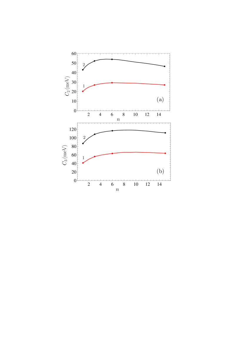
In Fig. 2(a) we present the computational results for the van der Waals coefficient in the free energy (7) as a function of the number of atomic layers of a Au film. The values of marked by dots on the solid and dashed lines labeled 1 were computed using the anisotropic dielectric permittivity of Fig. 1 by fully relativistic Eq. (8) and in the nonrelativistic limit (11), respectively. These results refer to the Au films consisting of and 15 atomic layers. For these films the anisotropic dielectric permittivities used in computations have been found in Ref. [16, ]. The values of coefficient for the intermediate values of were obtained by means of interpolation. The fully relativistic values of the van der Waals coefficient for the Au films, consisting of atomic layers are listed in the second column of Table I. As is seen in Fig. 2(a) (lines labeled 1), the relativistic effects contribute to the Casimir energy of the film considerably starting from atomic layers. Thus, the relative error of the nonrelativistic value of , defined as
| (13) |
quickly increases with increasing : %, 6.4%, 14.5%, and 43.7% for and 15, respectively.
The solid and dashed lines labeled 2 in Fig. 2(a) were computed using the bulk dielectric permittivity of Au by Eq. (8) in the relativistic case and by Eq. (11) in the nonrelativistic limit, respectively. From a comparison of the solid lines 1 and 2 in Fig. 2(a) it is seen that the anisotropy of dielectric properties results in important contribution to the Casimir energy of the atomically thin Au films. Thus, for films consisting of and 15 atomic layers the ratio of the van der Waals coefficients obtained using the isotropic and anisotropic dielectric permittivities is equal to 1.73, 1.37, 1.25, and 1.17, respectively. This means, for instance, that for the one- and three-layer films the respective deviation of the Casimir energy caused by a neglect of anisotropy is equal to 73% and 37%, respectively. The influence of film anisotropy practically disappears only for the films consisting of layers which corresponds to approximately 7 nm thickness.
Similar results can be obtained for the Casimir (van der Waals) pressure of an atomically thin metallic film. The Casimir pressure for the configurations under consideration is found from Eq. (1)
| (14) |
where the reflection coefficients are defined in Eq. (3).
In terms of the dimensionless variables introduced above, Eq. (14) takes the form convenient for numerical computations
| (15) |
where the van der Waals coefficient is given by
| (16) |
Here, the reflection coefficients are presented in Eq. (9).
In the nonrelativistic limit Eq. (16) is simplified to
| (17) |
and the reflection coefficients are defined in Eq. (10). Similar to the case of the van der Waals energy, for sufficiently thin films the substitution (12) can be made in both Eqs. (16) and (17). In so doing the computational results do not depend on .
The solid and dashed lines labeled 1 in Fig. 2(b) present the computational results for the van der Waals coefficient found from Eqs. (16) and (17), respectively. The computations have been performed for Au films of and 15 atomic layers, using the anisotropic dielectric permittivity of Ref. [16, ]. The obtained values of were interpolated for the intermediate numbers of layers. The fully relativistic values of are listed in the third column of Table I. The relative error in the nonrelativistic values of defined similar to Eq. (13) is equal to %, 2.3%, 5.8%, and 19.6% for Au films consisting of and 15 atomic layers, respectively. One can conclude that for the van der Waals pressure the relativistic effects are somewhat less than for the van der Waals energy.
The solid and dashed lines labeled 2 in Fig. 2(b) show the values of the van der Waals coefficient computed using the bulk dielectric permittivity of Au by Eqs. (16) and (17), respectively. Just as for the van der Waals energy, the role of relativistic effect increases with increasing film thickness. The role of anisotropy in the dielectric properties is also almost the same as for the van der Waals energy. From a comparison of the solid lines 1 and 2 in Fig. 2(b), for the ratio of the van der Waals coefficients , obtained using the isotropic and anisotropic , one finds 1.70, 1.35, 1.22, and 1.13 for and 15, respectively. Thus, in quantitative determination of the Casimir interaction of the atomically thin Au films, it is necessary to take into account an anisotropy of the dielectric permittivity of Au.
III Gold film on a substrate
Here, we consider an atomically thin Au film deposited on a thick dielectric substrate. In this case all the above equations apply with and equal to the dielectric permittivity of the substrate material. As an example, we consider the substrate made of Al2O3 (sapphire). The dielectric permittivity of sapphire at the imaginary Matsubara frequencies allows rather precise analytic representation27
| (18) |
where , , rad/s, and rad/s.
Numerical computations of the van der Waals coefficient defining the van der Waals (Casimir) energy (7) have been performed by Eq. (8) in the fully relativistic case using the anisotropic dielectric permittivity of Ref. [16, ]. The computational results are shown in Fig. 3(a) as four dots labeled 1 for the Au films consisting of and 15 atomic layers, respectively. The values of for films consisting of the intermediate numbers of layers were obtained by means of the interpolation procedure. They are listed in the fourth column of Table I. We have also performed respective computations in the nonrelativistic limit using Eq. (11). For an atomically thin Au film deposited on a sapphire substrate the relative error in the nonrelativistic values of defined in Eq. (13) for and 15 is equal to %, 7.3%, 15.0%, and 40.5%, respectively. This means that the relativistic effects contribute to the van der Waals energy significantly even for very thin films.
For comparison purposes, the line 2 in Fig. 3(a) reproduces the fully relativistic computational results for the van der Waals coefficient of a free-standing Au film [in Fig. 2(a) this line is labeled 1]. As is seen in Fig. 3(a), the magnitudes of the van der Waals energy of atomically thin Au films deposited on a sapphire substrate are considerably smaller than that of a free-standing film. Thus, the ratio of the respective van der Waals coefficients is equal to 0.47, 0.52, 0.54, and 0.58, for the Au films consisting of and 15 atomic layers, respectively. This means that the deposition on a dielectric substrate considerably decreases the van der Waals energy of the atomically thin Au films.
We have also performed numerical computations of the van der Waals coefficient for thin Au films deposited on a sapphire substrate. This coefficient determines the van der Waals (Casimir) pressure (15). The fully relativistic results computed by Eq. (16) using the anisotropic dielectric permittivity of Ref. [16, ] are shown as four dots labeled 1 in Fig. 3(b) for and 15 atomic layers, respectively. Together with the interpolated values of for other , they are included in the fifth column of Table I. The nonrelativistic values of for a thin Au film deposited on a sapphire substrate were calculated by Eq. (17). The relative error in the nonrelativistic values of is equal to %, 2.9%, 6.4%, and 19.0% for the Au films consisting of and 15 atomic layers, respectively.
The four dots and the line labeled 2 in Fig. 3(b) reproduce the computational results for the van der Waals coefficient of a free-standing in vacuum Au film [this line was labeled 1 in Fig. 2(b)]. As is seen in Fig. 3(b), the deposition on a sapphire substrate considerably decreases the van der Waals pressure of thin Au films. Quantitatively, the ratio of the van der Waals coefficients in the presence and in the absence of a sapphire substrate is equal to 0.48, 0.52, 0.54, and 0.57 for the Au films consisting of and 15 atomic layers, respectively. This opens opportunities to control the Casimir energy and pressure of the atomically thin metallic films.
IV Conclusions and discussion
In the foregoing we have investigated the van der Waals (Casimir) energies and pressures of metallic films consisting of only a few atomic layers with account of anisotropy of their dielectric properties. For this purpose, the dielectric tensor of Au obtained in Ref. [16, ] using the density functional theory was employed. Both the cases of free-standing films and films deposited on a substrate were considered. Although metallic films consisting of several atomic layers are not two-dimensional systems in a the strict sense, they are somewhat analogous to graphene because are described by the in-plane and out-of-plane dielectric permittivities (recent progress in calculation of the Casimir interaction in graphene systems28 ; 29 ; 30 ; 31 ; 32 ; 33 ; 34 ; 35 ; 36 resulted in explicit expressions for the dielectric functions of graphene in terms of the polarization tensor in (2+1)-dimensional space-time39 ; 40 ; 41 ; 42 ; 43 ; 44 ; 45 ; 46 ). Similar to the case of graphene, we have demonstrated that for atomically thin metallic films the effect of anisotropy contributes considerably to their van der Waals (Casimir) energy and pressure and cannot be neglected.
Numerical computations performed for thin Au films demonstrated that their actual van der Waals energies and pressures are much less than those computed using the bulk dielectric permittivity. Thus, for the free-standing Au films consisting of one and three atomic layers the relative error in the van der Waals energy per unit area arising from the use of bulk dielectric permittivity is equal to 73% and 37%, respectively (similar results hold for the Casimir pressure). This error decreases in magnitude with increasing number of atomic layers. According to our results, the bulk (isotropic) dielectric permittivity of Au becomes applicable only for films consisting of more than 30 atomic layers (i.e., for more than approximately 7 nm film thickness). We have also computed the van der Waals (Casimir) energies and pressures for a thin Au film deposited on a sapphire substrate and tabulated the energy and pressure van der Waals coefficients in both configurations considered for films consisting from 1 to 15 atomic layers.
To investigate the role of relativistic effects in the Casimir energy and pressure of atomically thin Au films, we have performed numerical computations in the nonrelativistic limit. It was shown that for a free-standing Au film the nonrelativistic results for the van der Waals energy are burdened by the relative error equal to 2.0% and 6.4% even for one- and three-layer films, respectively. The error increases to 43.7% for the Au film consisting of 15 atomic layers (similar errors arise in the nonrelativistic Casimir energy for a Au film deposited on a sapphire substrate). The nonrelativistic values of the Casimir pressure for thin films are somewhat more exact. Thus, for the one- and three-layer free-standing Au films the respective error is equal to 0.8% and 2.3%. For the film consisting of 15 atomic layers, the error in the nonrelativistic Casimir pressure increases up to 19.6%.
To conclude, we have shown that quantitative description of the van der Waals (Casimir) energies and pressures of atomically thin metallic films, both the free-standing and deposited on substrates, requires an account of anisotropy in their dielectric properties. Taking into account the wide application area of such films discussed in Sec. I, these results can be useful in development of novel heterostructures, semiconductor and nanoscale devices.
Acknowledgments
The authors are greatly indebted to Bo E. Sernelius for providing the numerical data of Fig. 1(a,b) in Ref. [16, ]. We are grateful also to L. B. Boinovich for attracting our attention to the problem of the van der Waals energy of thin films.
References
- (1) V. A. Parsegian, Van der Waals Forces: a Handbook for Biologists, Chemists, Engineers, and Physicists (Cambridge University Press, Cambridge, 2005).
- (2) M. Bordag, G. L. Klimchitskaya, U. Mohideen, and V. M. Mostepanenko, Advances in the Casimir Effect (Oxford University Press, Oxford, 2015).
- (3) G. L. Klimchitskaya, U. Mohideen, and V. M. Mostepanenko, Rev. Mod. Phys. 81, 1827 (2009).
- (4) R. H. French, V. A. Parsegian, R. Podgornik, et al., Rev. Mod. Phys. 82, 1887 (2010).
- (5) A. W. Rodriguez, F. Capasso, and S. G. Johnson, Nature Photon. 5, 211 (2011).
- (6) Q. Fu and T. Wagner, Surf. Sci. Rep. 62, 431 (2007).
- (7) K. F. Mak, C. Lee, J. Hone, J. Shan, and T. F. Heinz, Phys. Rev. Lett. 105, 136805 (2010).
- (8) A. Manjavacas and F. J. Garcia de Abajo, Nature Commun. 5, 3548 (2014).
- (9) J. Zou, Z. Marcet, A. W. Rodriguez, M. T. H. Reid, A. P. McCauley, I. I. Kravchenko, T. Lu, Y. Bao, S. G. Johnson, and H. B. Chan, Nature Commun. 4, 1845 (2013).
- (10) L. Boinovich and A. Emelyanenko, Adv. Colloid Interface Sci. 165, 60 (2011).
- (11) A. Benassi and C. Calandra, J. Phys. A: Math. Theor. 40, 13453 (2007).
- (12) A. Benassi and C. Calandra, J. Phys. A: Math. Theor. 41, 175401 (2008).
- (13) R. D. Loly and J. B. Pendry, J. Phys. C 16, 423 (1986).
- (14) C. Kittel, Introduction to Solid State Physics (Wiley, Hoboken, 2005).
- (15) A. Benassi and C. Calandra, Eur. Phys. Lett. 82, 61002 (2008).
- (16) M. Boström, C. Persson, and Bo E. Sernelius, Eur. Phys. J. B 86, 43 (2013).
- (17) Handbook of Optical Constants of Solids, ed. E. D. Palik (Academic, New York, 1985).
- (18) A. Šarlah and S. Žumer, Phys. Rev. E 64, 051606 (2001).
- (19) V. M. Mostepanenko, Phys. Rev. A 92, 012511 (2015).
- (20) R. S. Decca, E. Fischbach, G. L. Klimchitskaya, D. E. Krause, D. López, and V. M. Mostepanenko, Phys. Rev. D 68, 116003 (2003).
- (21) R. S. Decca, D. López, E. Fischbach, G. L. Klimchitskaya, D. E. Krause, and V. M. Mostepanenko, Ann. Phys. (N. Y.) 318, 37 (2005).
- (22) R. S. Decca, D. López, E. Fischbach, G. L. Klimchitskaya, D. E. Krause, and V. M. Mostepanenko, Phys. Rev. D 75, 077101 (2007).
- (23) R. S. Decca, D. López, E. Fischbach, G. L. Klimchitskaya, D. E. Krause, and V. M. Mostepanenko, Eur. Phys. J. C 51, 963 (2007).
- (24) C.-C. Chang, A. A. Banishev, R. Castillo-Garza, G. L. Klimchitskaya, V. M. Mostepanenko, and U. Mohideen, Phys. Rev. B 85, 165443 (2012).
- (25) A. A. Banishev, G. L. Klimchitskaya, V. M. Mostepanenko, and U. Mohideen, Phys. Rev. Lett. 110, 137401 (2013).
- (26) A. A. Banishev, G. L. Klimchitskaya, V. M. Mostepanenko, and U. Mohideen, Phys. Rev. B 88, 155410 (2013).
- (27) G. Bimonte, D. López, and R. S. Decca, arXiv:1509.05349v2.
- (28) G. L. Klimchitskaya and V. M. Mostepanenko, Phys. Rev. A 92, 042109 (2015).
- (29) L. Bergström, Adv. Colloid Interface Sci. 70, 125 (1997).
- (30) G. Gómez-Santos, Phys. Rev. B 80, 245424 (2009).
- (31) D. Drosdoff and L. M. Woods, Phys. Rev. B 82, 155459 (2010).
- (32) D. Drosdoff and L. M. Woods, Phys. Rev. A 84, 062501 (2011).
- (33) T. E. Judd, R. G. Scott, A. M. Martin, B. Kaczmarek, and T. M. Fromhold, New. J. Phys. 13, 083020 (2011).
- (34) Bo E. Sernelius, Phys. Rev. B 85, 195427 (2012).
- (35) A. D. Phan, L. M. Woods, D. Drosdoff, I. V. Bondarev, and N. A. Viet, Appl. Phys. Lett. 101, 113118 (2012).
- (36) M. Bordag, G. L. Klimchitskaya, and V. M. Mostepanenko, Phys. Rev. B 86, 165429 (2012).
- (37) G. L. Klimchitskaya and V. M. Mostepanenko, Phys. Rev. B 87, 075439 (2013).
- (38) G. L. Klimchitskaya and V. M. Mostepanenko, Phys. Rev. B 89, 035407 (2014).
- (39) M. Bordag, I. V. Fialkovsky, D. M. Gitman, and D. V. Vassilevich, Phys. Rev. B 80, 245406 (2009).
- (40) I. V. Fialkovsky, V. N. Marachevsky, and D. V. Vassilevich, Phys. Rev. B 84, 035446 (2011).
- (41) G. L. Klimchitskaya, V. M. Mostepanenko, and Bo E. Sernelius, Phys Rev. B 89, 125407 (2014).
- (42) G. L. Klimchitskaya and V. M. Mostepanenko, Phys. Rev. B 91, 045412 (2015).
- (43) M. Bordag, G. L. Klimchitskaya, V. M. Mostepanenko, and V. M. Petrov, Phys. Rev. D 91, 045037 (2015).
- (44) G. L. Klimchitskaya and V. M. Mostepanenko, Phys. Rev. B 91, 174501 (2015).
- (45) G. L. Klimchitskaya, C. C. Korikov, and V. M. Petrov, Phys. Rev. B 92, 125419 (2015).
- (46) M. Bordag, I. Fialkovsky, and D. Vassilevich, arXiv:1507.08693.
| Au film in vacuum | Au film on sapphire | |||
|---|---|---|---|---|
| (MeV) | (MeV) | (MeV) | (MeV) | |
| 1 | 42.9 | 86.8 | 20.3 | 41.3 |
| 2 | 49.0 | 100.0 | 24.7 | 50.0 |
| 3 | 52.2 | 108.5 | 27.0 | 56.3 |
| 4 | 53.7 | 112.8 | 28.2 | 59.5 |
| 5 | 54.1 | 115.1 | 29.0 | 61.8 |
| 6 | 53.9 | 116.7 | 29.4 | 63.4 |
| 7 | 53.6 | 117.8 | 29.3 | 65.1 |
| 8 | 52.8 | 118.2 | 29.1 | 66.1 |
| 9 | 51.9 | 118.3 | 29.0 | 66.2 |
| 10 | 51.0 | 118.0 | 28.9 | 66.5 |
| 11 | 50.3 | 117.8 | 28.5 | 66.1 |
| 12 | 49.5 | 115.8 | 28.2 | 65.8 |
| 13 | 48.6 | 114.2 | 27.8 | 65.2 |
| 14 | 47.6 | 112.8 | 27.5 | 64.6 |
| 15 | 46.5 | 111.8 | 27.1 | 63.9 |