Ultrafast exciton relaxation in monolayer transition metal dichalcogenides
Abstract
We examine a mechanism by which excitons undergo ultrafast relaxation in common monolayer transition metal dichalcogenides. It is shown that at densities 1 1011 cm-2 and temperatures K, excitons in well known monolayers (MoS2, MoSe2, WS2 and WSe2) exist as point-like structureless electron-hole quasi-particles. We evaluate the average rate of exciton energy relaxation due to acoustic phonons via the deformation potential and the piezoelectric coupling mechanisms and examine the effect of spreading of the excitonic wavefunction into the region perpendicular to the monolayer plane. Our results show that the exciton relaxation rate is enhanced with increase in the exciton temperature, while it is decreased with increase in the lattice temperature. Good agreements with available experimental data are obtained when the calculations are extrapolated to room temperatures. A unified approach taking into account the deformation potential and piezoelectric coupling mechanisms shows that exciton relaxation induced by phonons is as significant as defect assisted scattering and trapping of excitons by surface states in monolayer transition metal dichalcogenides.
I Introduction
In recent years, several works have examined the occurrences of large exciton binding energies ugeda2014giant ; hill2015observation ; makatom ; chei12 ; komsa2012effects ; thiljap as well as exciton mediated ultrafast processes mannebach2014ultrafast ; konabe2014effect ; wang2014ultrafast that are enhanced in atomically thin layered transition metal dichalcogenides MX2 (M = Mo, W, Nb, and X = S, Se) wilson ; wang ; he2014stacking . The monolayer Molybdenum and Tungsten dichalcogenides (MoS2, MoSe2, WS2 and WSe2) generally have similar lattice parameters and electronic configurations liu2015electronic ; mann20142 . Transition metal dichalcogenides are known to undergo a crossover from indirect band gap (bilayer) to direct gap in the monolayer configuration makatom where there is strong photoluminescence. The intrinsic band gap range from 0.5 eV to 2 eV, depending on the material composition and number of layers in the material system. Specifically, the confinement of charge carriers within a monolayer space results in an enhanced interaction of the exciton with light, a desirable property that can be exploited to fabricate highly sensitive photodetectors and sensor devices.
The study of exciton based quantum dynamical processes is important as excitonic interactions underlie the unique optoelectronic properties kumar2014tunable ; komsa2012effects ; qiu2013 ; jariwala2014emerging ; qiu2015nonanalyticity of monolayer dichalcogenides. Several applications lembke2015single ; pospischil2014solar ; zhang2014m ; tsai2014monolayer ; radisavljevic2011integrated ; yoon2011good can be linked to the rich many-body effects of excitons in low-dimensional transition metal dichalcogenides. The long lifetimes of excitons in transition metal dichalcogenides enable interaction with additional degrees of freedom linked to the unique optical selection rules of the momentum valleys xiao2012coupled ; suzuki2014valley of two-dimensional MX2 materials. This enables tuning of the coupling strength of the valley to spin degrees of freedom. which results in desirable valleytronics properties mai2013many essential for high speed logic devices A comprehensive understanding of the quantum dynamical processes of two-dimensional excitons is needed to fully exploit the unique properties of monolayer transition metal dichalcogenides for electrooptical and valleytronic devices
Exciton dynamics in monolayer and few-layer MoS2 2D crystals examined using femtosecond transient absorption spectroscopy and microscopy techniques shi2013exciton show a highly enhanced intraband relaxation rate 0.5 ps in the monolayer configuration compared to 20 ps in the bulk material. This enhanced relaxation rate was attributed to increased defect assisted scattering and trapping of excitons by surface states shi2013exciton . The rapid capture rates of excitons by mid-gap defects from Auger processes was estimated to be about less than a picosecond to a few picoseconds in monolayer metal dichalcogenides wang2015fast . The capture rates which display both linear and quadratic dependences on the exciton density arises primarily from the large overlap of the defect state wavefunction with the conduction or valence band Bloch state wavefunctions. The exciton capture rates are almost comparable to the exciton-exciton annihilation (EEA) rates sun2014observation ; konabe2014effect that becomes dominant as a result of the reduced Coulomb screening of spatially confined charge carriers in layered transition metal dichalcogenides.
The layered structures of metal chalcogenides give rise to a variety of phonon modes that interact via short range and long range forces with unique thickness dependences of phonons in layered transition metal dichalcogenides lee ; zhao13inter ; chakraborty2013layer . There exist two Raman active modes, and which exhibit frequency shifts with layer thickness in MoS2 lee ; mol11phonons ; zhao13inter . The mode is associated with the out-of-plane displacement of S atoms while the is associated with the in-plane but opposing displacements of Mo and S atoms lee ; mol11phonons . Photoluminescence studies of single-layer MoS2 korn2011low reveal a long-lived component due to exciton-phonon scattering, which highlights the importance of exciton interaction with phonons. The occurrence of interface and confined slab phonon modes hai1993electron and dimensionality dependent exciton-phonon interactions in low-dimensional material systems thilagam1997exciton has not been fully examined in monolayer metal dichalcogenides. To this end, the possibility of an enhanced exciton relaxation arising from phonon assisted mechanism remains to be explored in few-layer transition metal dichalcogenide systems. In this study we consider the critical role played by phonons during exciton relaxation processes and compare computed rates of exciton energy relaxation with estimates of enhanced exciton relaxation rates associated with surface defects shi2013exciton ; wang2015fast in monolayer and few-layer samples.
In the monolayer transition-metal dichalcogenides, a direct band gap between the conduction and valence band extrema occurs at the point. While an energy minimum occurs at the point along the axis at the lowest conduction band, energy is maximized at the point of the valence band jin2014intrinsic . Charge carriers are generally located in the conduction band valleys which are approximately parabolic for energies less than 300 eV chei12 . The direct excitonic transitions are enhanced at the two extremal locations of the point in the monolayer configuration. Newly formed quasi-two-dimensional excitons that possess a finite center-of-mass motion momentum wave vector undergo one of four main processes : (1) jump to higher energy band states via absorption of phonons, (2) relax to lower kinetic energies via emission of phonons, (3) decay non-radiatively or radiatively to the continuum state and lastly (4) decay into free electron and holes that subsequently relax via phonon emission to lower energy levels.
In this study, we consider that newly formed electron-hole pairs lose energy via emission of longitudinal-acoustic (LA) and/or transverse-acoustic (TA) phonons via the deformation potential coupling channel. The exciton relaxation is initiated by deformations of the lattice potentials by acoustic phonons which is applicable at the low temperature range. The low dimensional excitons are considered to undergo further energy relaxation along the exciton dispersion curves before reaching a minimum in exciton energy. The temperature range of 5 70 K considered here therefore excludes the possibility of exciton relaxation via optical phonon modes as these transitions involve higher energies. Piezoelectricity which arises from the linear coupling between the electrical polarization and mechanical strain within a crystal have reasonable strengths in monolayer metal dichalcogenides alyoruk2015 ; yin2014observation ; duerloo2013 ; reed2015 . The two-dimensional hexagonal crystal structure lacks an inversion symmetry, hence there occurs a strain field which gives rise to the piezoelectric properties in transition metal dichalcogenides. We therefore include the scattering of exciton due to the piezoelectric coupling via acoustic phonons in this study.
The paper is organized as follows. In Sec. II, we present the theoretical form of exciton wavefunction which is suitable for modeling the correlated electron-hole pair in monolayer transition metal dichalcogenides. In Sec. III, we discuss the Maxwell-Boltzmann and Bose-Einstein exciton distributions, and justify our choice of a suitable exciton distribution based on the material properties of the monolayer dichalcogenides given in Table-I. We also discuss the conditions required for a statistically degenerate system of excitons to occur in monolayer systems. In Sec. IV we present an explicit form of a quasi-two dimensional exciton-acoustic phonon interaction operator applicable in monolayer systems. This operator is used to derive the average rate of exciton energy relaxation, in Sec. V. Numerical results are presented for the monolayer transition metal dichalcogenides, MoS2, MoSe2, WS2 and WSe2 and differences in their relaxation properties are analyzed in Sec. V. The theory of exciton relaxation due to the piezoelectric coupling mechanism is presented in Sec. VI along with analysis of numerical results based on the piezoelectric properties of transition metal dichalcogenides. Lastly, conclusions are summarized in Sec. VII.
II Exciton wavefunction in the monolayer transition metal dichalcogenides
In transition metal dichalcogenides (MX2) the intra-layers of the M metal planes are held between the chalcogen X atomic planes by covalent bonding. The inter-layers can be easily separated into distinct layers cho2008 ; mouri2013 of just a few atomic layers. A hexagonally ordered plane of metal atoms sandwiched between two other hexagon planes of chalcogen atom represents a single monolayer which we examine using a quasi two-dimensional space. This is justified as the motion of the exciton is mostly confined within the parallel two-dimensional layers of the atomic planes and there is restricted exciton motion in the direction perpendicular to the monolayer plane. Accordingly, the exciton is represented by a quasi-two dimensional wavefunction thilagam2015excitonic , and for simplicity we introduce the two-band approximation involving the lowest electron subband and highest hole subband structure. The exciton state vector denoted by in the presence of phonons can then be written as
| (1) |
where is the volume of the unit cell and is a quantized length of the lattice space. We restrict this study to the the lowest exciton state without great loss in generality. The co-ordinate of the centre of mass of an exciton, is given by
| (2) | |||||
| (3) |
where ( ) is the effective mass of the electron (hole). The position vectors and wave vectors are decomposed into components parallel and perpendicular to the monolayer plane as and respectively. The creation operator of an electron in the conduction band at position is denoted by . The annihilation operator of an electron in the valence band at position is denoted by . The state in Eq.1 is given by
| (4) |
where is the electronic vacuum state of the system that represents completely filled valence bands and empty conduction bands. The occupation number of phonons with wavevector is given by
| (5) |
In Eq.1, denotes the th state exciton envelope function in the in the monolayer configuration. This state has the variational envelope function which appear as taka2
| (6) |
where is the normalization constant and is the relative separation of the electron-hole pair in the monolayer plane. We have assumed that the excitonic wavefunction undergoes a discontinuous transition to zero beyond the region and , where is the average displacement of electrons and holes in the direction. perpendicular to the monolayer surface. The parameters and are determined by minimalizing the energy of the exciton in the presence of phonons, a task that is not numerically trivial. We therefore treat and as adjustable parameters that appear as inverses of the confinement lengths parallel and perpendicular to the monolayer plane. For the exact two dimensional case, = 0.
III Maxwell-Boltzmann versus Bose-Einstein exciton distributions
The results of exciton relaxation kinetics is very much dependent on the type of exciton distribution employed during the modeling process. A widely used distribution is the Maxwell-Boltzmann function which appear as
| (9) |
where denotes the exciton temperature and is the boltzmann constant. The total number of excitons can be easily evaluated as
| (10) |
where is the quantization length and is the exciton mass. The distribution in Eq.10 is applicable to the classical model of quasi-equilibrium of low dimensional excitons. The Maxwell-Boltzmann statistical distribution of excitons is suited for the temperature range, where the degeneracy temperature is given by ivanov1999bose
| (11) |
where is the exciton density, and the degeneracy factor = 4, expressed a product of the spin and valley degeneracy factors kaasbjerg12 .
The exciton distribution function based on the Bose-Einstein distribution is given by
| (12) | |||||
| (13) |
where the quasi-two dimensional exciton chemical potential is dependent on the exciton temperature and exciton density ivanov1999bose . We evaluate the total number of excitons as
| (14) | |||||
From Eq. 14, it is seen that the Bose-Einstein distribution of excitons is the most appropriate model at low temperatures for which there exist a large exciton population with small wavevectors.
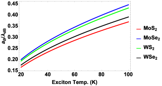
In the case of MoS2, we substitute the exciton density, = 1 1011 cm-2, and = 0.51, =0.58 jin2014intrinsic in Eq.11 which gives = 1.3 K. The exciton density of 1 1011 cm-2 corresponds to an inter-particle distance of 316 Å, which is about 35 times the size of the exciton radius of 9 Åthiljap . Thus at typical exciton temperatures greater than 10 K, the excitons in the MoS2 monolayer can be considered as well-defined correlated electron-hole quasi-particles. Excitons can also be modeled as point-like structureless systems provided the exciton de Broglie wavelength () far exceeds the exciton Bohr radius . Based on the material properties of the monolayer transition metal dichalcogenides, MoS2, MoSe2, WS2 and WSe2 (given in Table-I), the ratio is plotted as a function of the exciton temperature in Fig. 1a. There are subtle differences due to varying material properties of the four types of monolayer systems. In general, the Maxwellian distribution appears appropriate for comparatively low exciton temperatures, K and moderate exciton densities, 1011 cm-2 (see Fig. 1b). We therefore restrict to the classical temperature range and exciton concentration to examine the exciton relaxation pathways in this study.
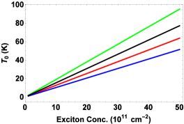
In Fig. 1b, the degeneracy temperature (Eq.11) is plotted as a function of the exciton density , for MoS2, MoSe2, WS2 and WSe2. The and values used in the calculations are retrieved from Ref. jin2014intrinsic (see Table-I). Tungsten sulphide yields the highest estimate of which can be partly attributed to its comparatively small exciton mass (+ ). The sulfides possess a higher than the selenides. The results in Fig. 1 show that at high enough exciton densities 1012 cm-2, there is possible occurrence of a statistically degenerate system of excitons. This gives rise to relaxation mechanisms that are dependent on the Bose-Einstein statistical distribution of the excitons. In this study, we choose a lower density = 1 1011 cm-2 so as to exclude degenerate effects.
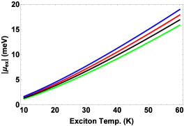
Applying Eq.13 to the monolayer MoS2, we obtain the negative exciton chemical potential = -4.8 meV at exciton temperature = 20 meV and the density, = 1 1011 cm-2. The chemical potential assumes negative values of magnitude larger than 5 meV for 20 meV, hence condensation processes can be excluded at typical operating conditions shi2013exciton ; wang2015fast in MoS2. In Fig. 1 c, the absolute value of the exciton chemical potential, is plotted as a function of the exciton temperature with exciton density fixed at = 1.5 1011 cm-2 for all the dichalcogenides. Molybdenum selenide yields the highest estimate of due to its comparatively large exciton mass (+ ). The selenides show slightly higher than the sulfides, while the Molybdenum dichalcogenides have higher than the Tungsten dichalcogenides.
IV Quasi-two dimensional exciton-acoustic phonon interaction operator
The three dimensional electron-phonon interaction due to the deformation-potential coupling can be written as
| (15) |
where and are the deformation potentials for the conduction and valence bands, is the mass density of the bulk system and is the sound velocity of the longitudinal-acoustic phonon mode in the material. The phonon creation and annihilation operators are indicated by and respectively. An explicit form of the quasi-two dimensional operator can be obtained by projecting the matrix element of the three dimensional electron-phonon interaction operator between two quasi-two dimensional exciton states taka2 . This approach assumes that the electron-hole internal motion remains unchanged during interaction with the phonons.
Using the wave function in Eq. (6), and the exciton state vector specified in Eqs. (7) and (8), the quasi-two dimensional exciton-phonon interaction operator can be obtained using Eq. (15)
| (16) |
where and . The term is the surface area of the monolayer plane, is the areal mass density and is the sound velocity of the phonon mode in the monolayer system. The delta function in Eq. (16) conserves the momentum of the scattered exciton and phonon along the plane. The function is given by taka2
| (17) |
The explicit form of the function is lengthy and we therefore derive at specific values of . At the limits and the function take simple forms
| (18) | |||||
| (19) |
V Relaxation of exciton kinetic energy
At low lattice temperatures ( 30 K), the exciton relaxes by losing its kinetic energy along the dispersion energy curves coupled with the emission of acoustic phonons. The overall rate at which phonons are emitted is dependent on the energy exchanges between the exciton and phonon during the intra-valley relaxation process. The net increase in the number of acoustic phonons is based on the emission rate of phonons with wave vector
| (21) |
where the thermalized average occupation of phonons , and is the energy of phonon with wavevector . The term denotes the distribution function associated with the exciton wave vector . During exciton scattering, the energy conservation rule is obeyed, where . The angle between the exciton wave vector and is denoted by .
The relation in Eq. 22 can be further simplified by assuming the action of comparatively large phonon wave vectors such that where to the following form
| (22) |
where . Substituting Eqs.9 and 10 into Eq.22, we obtain an expression for the average rate of exciton energy relaxation
| (23) | |||||
| (24) |
To obtain an explicit expression for the average rate of exciton energy relaxation in Eq.23, we employ the form of the quasi- two dimensional exciton-phonon interaction term in Eq.16
| (25) | |||||
| (26) |
where . To simplify the numerical evaluation of , we use , which does not affect the order of magnitude of the energy relaxation rate. Using the explicit form for derived using Eq.17, we numerically evaluate for the four monolayer transition metal dichalcogenides, MoS2, MoSe2, WS2 and WSe2 based on the material parameters provided in Table-I.
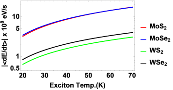
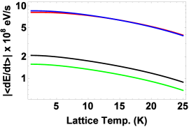
Fig. 2a shows the increase in with exciton temperature for various monolayer transition metal dichalcogenides at a given lattice temperature = 5 K and confinement parameter = 0.25. The energy relaxation rates for MoS2 lies in the range eV/s for exciton temperatures less than 60 K. The phonon induced relaxation rates when extrapolated to higher temperatures with assumption of the Maxwellian distribution for excitons, match the experimental estimates of about eV/s observed at room temperatures. The experimental results were previously attributed to defects assisted intra-band scattering processes shi2013exciton . We point out that only the relaxation channel via LO-phonons has been included to evaluate the results in Fig. 2a. We expect the additional channels provided by TO-phonons, as well scattering via piezoelectric coupling (Section VI) to further enhance exciton relaxation rates in monolayer systems. The results in Fig. 2 highlight the critical role played by acoustic phonons in inducing exciton relaxation processes and imply that exciton-phonon interactions can become as strong as exciton-defect interactions under favourable conditions.
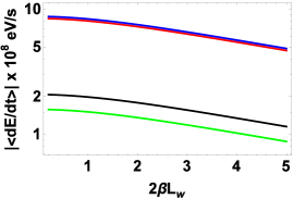
Fig. 2a shows that the Molybdenum dichalcogenides experience the fastest energy relaxation due to their high exciton effective masses, low mass densities and high deformation potential constants. Due to similar material properties, the estimated are approximately the same for MoS2 and MoSe2 monolayer systems. Fig. 2b displays the mean relaxation rate as function of the lattice temperature at the exciton temperature = 40K and = 0.25. The results indicate a decrease in the effectiveness of the exciton-acoustic phonon interaction channel as the lattice temperature is increased. The parameter yields a measure of confinement of the charge carriers in the direction perpendicular to the monolayer plane. The decline in with increase in in Fig. 2c shows that reduction in dimensionality enhances energy relaxation rates in monolayer systems.
VI Exciton relaxation due to the piezoelectric coupling mechanism
We express the piezoelectric exciton-phonon interaction operator in a form analogous to Eq.16 as
| (27) |
where () is the piezoelectric constant for the electron (hole), and is the dielectric constant that is independent of the piezoelectric effect. As given in Eq.16, is the areal mass density, is the sound velocity of the phonon mode in the monolayer system and , . Due to the coupling with the TA and LA phonons, piezoelectric interactions are anisotropic in nature. These anisotropic effects can be incorporated by considering the angular mean of the piezoelectric interaction, which introduces the factor in Eq.27.
The piezoelectric constant has been estimated to be C/m for monolayer MoS2 kaasbjergacou , which is an order of magnitude less than the estimate C/m provided by Duerloo et. al. duerlooemergent (Table-I). The reasons for the differences in the piezoelectric constant values for MoS2 from the two known sources kaasbjergacou ; duerlooemergent remain unresolved. According to the piezoelectric constants given in Ref.duerlooemergent , the Molybdenum dichalcogenides have higher piezoelectric strengths than the Tungsten dichalcogenides as can be seen in Table-I. So far all known piezoelectric constants kaasbjergacou ; duerlooemergent are linked to the linear coupling between the electrical polarization induced by the electron and strain field within the crystal. There is no mention of similar interactions associated with electrical polarization induced by the hole. In order to obtain numerical estimates of the exciton relaxation rates, we consider the difference = C/m where the parameter is varied from 0.1 to 1.5.
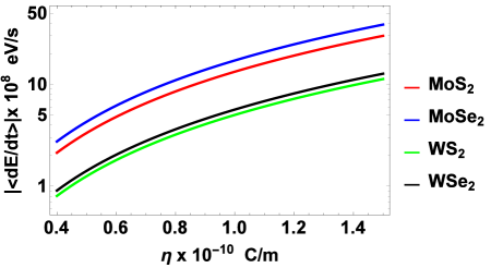
Using Eq.27 and the numerical scheme outlined in SectionV, we evaluate the average rate of exciton energy relaxation as a function of the difference in piezoelectric constants, C/m. The results evaluated by setting exciton temperature = 35 K, and lattice temperature, = 5 K are displayed in Fig. 3 for four monolayer transition metal dichalcogenides. In all materials, there is increase of with , and values for lie in the range eV/s for C/m. The order of rates evaluated in Fig. 3 are comparable to results in Fig. 2 computed previously for exciton-phonon interaction due to the deformation potential mechanism. These results indicate that a unified approach for exciton-phonon interactions taking into account both deformation potential and piezoelectric mechanisms will yield a higher rate of exciton relaxation than those shown in Figs 2, 3. The results obtained in this study imply that exciton relaxation induced by phonons can become as important as defects assisted intra-band scattering processes shi2013exciton . The role of exciton-exciton interactions during energy relaxation has not been considered in this work. An earlier work thilexci has shown that inter-excitonic interactions are sensitive to changes in the excitonic wavefunctions, indicating that such interactions may possibly be enhanced in monolayers compared to bulk systems. This can be attributed to the enhanced Coulomb coupling between electrons and holes. A detailed study of the role of inter-excitonic interactions on exciton-phonon interactions is beyond the scope of this work as this requires a refinement in the form of the variational envelope function employed in Eq.6. Nevertheless it would be worthwhile to examine whether exciton-exciton interactions will influence the phonon assisted exciton relaxation in future studies.
VII Conclusion
The confinement of excitons to a narrow region of space is an important property of monolayer structures that forms the basis for high excitonic binding energies and other desirable properties. In this work we have examined the relaxation of quasi-two dimensional excitons due to interactions with acoustic phonons via the deformation potential mechanism. The influence of piezoelectric coupling linked to electrostatic interaction between the acoustic phonons and the crystal polarisation field is also included in this study. The relaxation rates due to the corresponding scattering mechanisms are analyzed for common monolayer transition metal dichalcogenides (MoS2, MoSe2, WS2 and WSe2). The results obtained here indicate that exciton relaxation induced by phonons due to the deformation potential and piezoelectric coupling mechanisms are comparable to defects assisted intra-band scattering processes and trapping of excitons by surface states in monolayer transition metal dichalcogenides. The results also indicate that Molybdenum dichalcogenides undergo faster exciton energy relaxation than the Tungsten dichalcogenides.
The results obtained in this work have importance in the optimization of material properties for device applications and for further exploration of new ideas in physics for development of innovative optical and sensor devices. Future studies of the effects of phonons on the tunneling between valence and conduction band in a p-n junction tunnel based on MoS2 monolayer systems are expected to provide useful results relevant for device operations. The electronic structures of transition metal dichalcogenides are complex and highly sensitive to electric and magnetic fields. To this end, further investigations on the maneuverability of the electronic structures and the influence of external fields on exciton-phonon interaction is expected to provide an improved understanding of the origins of desirable properties that can be exploited in the development of new devices for future industries.
References
- (1) M. M. Ugeda et al., Nature materials 13, 1091 (2014).
- (2) H. M. Hill et al., Nano Letters 15, 2992 (2015).
- (3) K. F. Mak, C. Lee, J. Hone, J. Shan, and T. F. Heinz, Physical Review Letters 105, 136805 (2010).
- (4) T. Cheiwchanchamnangij and W. R. Lambrecht, Physical Review B 85, 205302 (2012).
- (5) H.-P. Komsa and A. V. Krasheninnikov, Physical Review B 86, 241201 (2012).
- (6) A. Thilagam, Journal of Applied Physics 116, 053523 (2014).
- (7) E. M. Mannebach et al., ACS Nano 8, 10734 (2014).
- (8) S. Konabe and S. Okada, Physical Review B 90, 155304 (2014).
- (9) H. Wang, C. Zhang, and F. Rana, Nano Letters 15, 339 (2014).
- (10) J. Wilson and A. Yoffe, Advances in Physics 18, 193 (1969).
- (11) Q. H. Wang, K. Kalantar-Zadeh, A. Kis, J. N. Coleman, and M. S. Strano, Nature Nanotechnology 7, 699 (2012).
- (12) J. He, K. Hummer, and C. Franchini, Physical Review B 89, 075409 (2014).
- (13) G.-B. Liu, D. Xiao, Y. Yao, X. Xu, and W. Yao, Chemical Society Reviews 44, 2643 (2015).
- (14) J. Mann et al., Advanced Materials 26, 1399 (2014).
- (15) A. Kumar and P. Ahluwalia, Tunable electronic and dielectric properties of molybdenum disulfide, in Mo, pp. 53–76, Springer, 2014.
- (16) D. Y. Qiu, H. Felipe, and S. G. Louie, Physical Review letters 111, 216805 (2013).
- (17) D. Jariwala, V. K. Sangwan, L. J. Lauhon, T. J. Marks, and M. C. Hersam, ACS Nano 8, 1102 (2014).
- (18) D. Y. Qiu, T. Cao, and S. G. Louie, Physical Review Letters 115, 176801 (2015).
- (19) D. Lembke, S. Bertolazzi, and A. Kis, Accounts of chemical research 48, 100 (2015).
- (20) A. Pospischil, M. M. Furchi, and T. Mueller, Nature nanotechnology 9, 257 (2014).
- (21) H. Zhang et al., Optics express 22, 7249 (2014).
- (22) M.-L. Tsai et al., ACS Nano 8, 8317 (2014).
- (23) B. Radisavljevic, M. B. Whitwick, and A. Kis, ACS Nano 5, 9934 (2011).
- (24) Y. Yoon, K. Ganapathi, and S. Salahuddin, Nano Letters 11, 3768 (2011).
- (25) D. Xiao, G.-B. Liu, W. Feng, X. Xu, and W. Yao, Physical Review Letters 108, 196802 (2012).
- (26) R. Suzuki et al., Nature nanotechnology 9, 611 (2014).
- (27) C. Mai et al., Nano Letters 14, 202 (2013).
- (28) H. Shi et al., ACS Nano 7, 1072 (2013).
- (29) H. Wang et al., Physical Review B 91, 165411 (2015).
- (30) D. Sun et al., Nano Letters 14, 5625 (2014).
- (31) C. Lee et al., ACS Nano 4, 2695 (2010).
- (32) Y. Zhao et al., Nano Letters 13, 1007 (2013).
- (33) B. Chakraborty, H. Matte, A. Sood, and C. Rao, Journal of Raman Spectroscopy 44, 92 (2013).
- (34) A. Molina-Sanchez and L. Wirtz, Physical Review B 84, 155413 (2011).
- (35) T. Korn, S. Heydrich, M. Hirmer, J. Schmutzler, and C. Schüller, Applied Physics Letters 99, 102109 (2011).
- (36) G. Hai, F. Peeters, and J. Devreese, Physical Review B 48, 4666 (1993).
- (37) A. Thilagam, Physical Review B 56, 9798 (1997).
- (38) Z. Jin, X. Li, J. T. Mullen, and K. W. Kim, Phys. Rev. B 90, 045422 (2014).
- (39) M. M. Alyoruk, Y. Aierken, D. Cakır, F. M. Peeters, and C. Sevik, The Journal of Physical Chemistry C 119, 23231 (2015).
- (40) H. Zhu, Y. Wang, J. Xiao, M. Liu, S. Xiong, Z. Wong, Z. Ye, Ziliang, Y. Ye, X. Yin, and X. Zhang, Xiang, Nature Nanotechnology 10, 151 (2015).
- (41) K.-A. N. Duerloo, M. T. Ong, and E. J. Reed, Piezoelectricity in monolayers and bilayers of inorganic two-dimensional crystals, in MRS Proceedings Vol. 1556, pp. Mrss13–1556, Cambridge Univ Press, 2013.
- (42) E. J. Reed, Nature nanotechnology 10, 106 (2015).
- (43) J. H. Cho et al., Nature materials 7, 900 (2008).
- (44) S. Mouri, Y. Miyauchi, and K. Matsuda, Nano Letters 13, 5944 (2013).
- (45) A. Thilagam, Physica B: Condensed Matter 464, 44 (2015).
- (46) T. Takagahara, Physical Review B 31, 6552 (1985).
- (47) A. Ivanov, P. Littlewood, and H. Haug, Physical Review B 59, 5032 (1999).
- (48) K. Kaasbjerg, K. S. Thygesen, and K. W. Jacobsen, Physical Review B 85, 115317 (2012).
- (49) K. Kaasbjerg, K. S. Thygesen, and A.-P. Jauho, Physical Review B 87, 235312 (2013).
- (50) K. Duerloo, M. Ong, and E. Reed. The Journal of Physical Chemistry Letters 3, 2871 (2012).
- (51) A. Thilagam, Physical Review B 63, 045321 (2001).
- (52) J. Kang, S. Tongay, J. Zhou, J. Li, and J. Wu, Applied Physics Letters 102, 012111 (2013).
- (53) Y. Ding et al., Physica B: Condensed Matter 406, 2254 (2011).
- (54) P. Solomon et al., Journal of Applied physics 95, 5800 (2004).
| System | , | (Å) | (Å) | (eV) | (eV) | cm/s | g/cm2 | C/m | Å | |
|---|---|---|---|---|---|---|---|---|---|---|
| MoS2 | 0.51, 0.58 | 3.18 | 3.13 | 4.5 | 2.5 | 6.6 | 1.56 | 3.64 | 0.006 | 7.5 |
| MoSe2 | 0.64, 0.71 | 3.32 | 3.35 | 3.4 | 2.8 | 4.1 | 2.01 | 3.92 | 0.005 | 8.0 |
| WS2 | 0.31, 0.42 | 3.18 | 3.14 | 3.2 | 1.7 | 4.3 | 2.36 | 2.71 | 0.003 | 10.6 |
| WSe2 | 0.39, 0.51 | 3.32 | 3.36 | 3.2 | 2.1 | 3.3 | 3.09 | 2.47 | 0.003 | 8.6 |