Subgap resonant quasiparticle transport in normal-superconductor quantum dot devices
Abstract
We report thermally activated transport resonances for biases below the superconducting energy gap in a carbon nanotube (CNT) quantum dot (QD) device with a superconducting Pb and a normal metal contact. These resonances are due to the superconductor’s finite quasi-particle population at elevated temperatures and can only be observed when the QD life-time broadening is considerably smaller than the gap. This condition is fulfilled in our QD devices with optimized Pd/Pb/In multi-layer contacts, which result in reproducibly large and “clean” superconducting transport gaps with a strong conductance suppression for subgap biases. We show that these gaps close monotonically with increasing magnetic field and temperature. The accurate description of the subgap resonances by a simple resonant tunneling model illustrates the ideal characteristics of the reported Pb contacts and gives an alternative access to the tunnel coupling strengths in a QD.
pacs:
73.23.Hk, 73.63.Kv, 74.45.+cQuantum phenomena in nanostructures with a superconductor (S) and a normal metal contact (N) coupled to low-dimensional electron systems like a quantum dot (QD)Gräber et al. (2004) have recently gained much attention due to potential applications in quantum technology. Especially prominent are transport phenomena at energies below the superconductor’s energy gap, , which typically comprise quasi-particle (QP) tunneling and Andreev processes due to Cooper pair transport. These processes result in a large variety of subgap features, for example Majorana Fermions,Mourik et al. (2012) which might be used for topological quantum computation,Das Sarma, Freedman, and Nayak (2015) Cooper pair splittingRecher, Sukhorukov, and Loss (2001); Hofstetter et al. (2009); Herrmann et al. (2010); Schindele, Baumgartner, and Schönenberger (2012); Das et al. (2012) as a source of entangled electrons, resonant and inelastic Andreev tunneling,Gramich, Baumgartner, and Schönenberger (2015) or Andreev bound states (ABSs)Pillet et al. (2010); Dirks et al. (2011); Lee et al. (2014); Schindele et al. (2014) which can be implemented as Andreev qubits.Bretheau et al. (2013); Janvier et al. (2015) Recent experiments have highlighted the importance to understand in detail the QP excitations in such structures, which, for example, lead to additional subgap features,Gaass et al. (2014); Ratz et al. (2014) or to a poisoning of the bound state parity lifetime.Higginbotham et al. (2015)
To identify subgap transport mechanisms, a transport gap much larger than the QD life time, , is very beneficial – a regime which is not easily achieved in S-QD hybrid devices. In addition, a strong suppression of the QP conductance in the subgap regime is required, which is commonly known as a “clean gap”. While the widely used superconductor AlHofstetter et al. (2009); Herrmann et al. (2010); Schindele, Baumgartner, and Schönenberger (2012) has yielded devices with good transport characteristics, long superconducting coherence lengths, , and more recently also clean gaps,Chang et al. (2015); Higginbotham et al. (2015); Taupin et al. (2016) it’s small gap renders spectroscopic investigations difficult. S-QD devices based on the large-gap superconductor Nb allowed the observation of several fundamental transport processesGrove-Rasmussen et al. (2009); Gaass et al. (2014); Ratz et al. (2014); Schindele et al. (2014); Gramich, Baumgartner, and Schönenberger (2015) and new effects due to the large critical field.Fülöp et al. (2015) However, Nb has rather short coherence lengths and the devices often exhibit strongly suppressed or “soft” gapsGrove-Rasmussen et al. (2009); Gaass et al. (2014); Fülöp et al. (2015) and complex magnetic field characteristics,Gramich, Baumgartner, and Schönenberger (2015); Fülöp et al. (2015) which make normal state control experiments difficult. In contrast, in the superconductor Pb one finds a large bulk coherence length of nm, a superconducting gap of meV, and a low critical field of mT.Poole (2000) In Pb-based devices large transport gaps have already been demonstrated for carbon nanotubes (CNTs) using tunnel barriersChen et al. (2009); Bronn and Mason (2013); Dirks et al. (2009) and allowed the observation of Cooper pair splitting in graphene.Borzenets et al. (2015) Here we present the growth and fabrication of well-defined, reproducible multi-layered Pb-based superconducting contacts to CNTs, which can be easily applied to other materials like graphene or semiconducting nanowires. We demonstrate reproducibly large and clean superconducting transport gaps in CNT QDs with a narrow Pb-based and a normal metal contact. While our fabrication scheme allows for different tunnel coupling strengths of the S contact to the QD due to an implemented Pd contact layer, we focus here solely on QP transport to demonstrate characteristics ideal for spectroscopy experiments. As an example, we report subgap transport resonances that originate from tunneling of thermally excited QPs through a CNT QD. These features were predicted recentlyWhan and Orlando (1996); Pfaller, Donarini, and Grifoni (2013) and reported for experiments in S-QD-S devices,Gaass et al. (2014); Ratz et al. (2014) whereas the lack of a large superconducting transport gap prohibited their observation in N-QD-S devices.
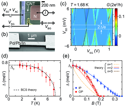
Figure 1(a) shows a false color scanning electron microscope (SEM) image of the N-QD-S device, including a schematic of the measurement setup. CNTs were grown by chemical vapor deposition on a highly p-doped Si/SiO2 substrate used as a backgate (BG). A subsequent surface treatment with radicals from an rf-induced hydrogen plasmaYang et al. (2010) leads to defect-free, clean CNTs for further processing.Schindele et al. (2014); Gramich, Baumgartner, and Schönenberger (2015) Using optimized electron beam lithography,Samm et al. (2014) we fabricate a nm wide S contact and an N contact at a distance of nm on a CNT, and a single sidegate (SG). We use nm of e-beam evaporated Pd for the N contact, SG, and for the outer leads and bonding pads of the narrow S contact. A direct, not optimized evaporation of Pb at room temperature (RT) typically results in a strong island growth, where oxidation between the grain boundaries can result in highly resistive normal conducting Pb strips. Here we deposit an optimized Pd/Pb/In (//nm) multi-layer in-situ as the last fabrication step using electron beam evaporation at a base pressure mbar with a Pb deposition rate of Å/s and a sample stage temperature of K. This favors a more uniform Pb growth and reduces Pb surface diffusion. In contrast to the tunnel barriers implemented in Refs. 26; 24; 25, we use a Pd wetting layer to the CNT which allows for some tunability of the S contact coupling strengths and for a smooth and homogeneous Pb growth, see Fig. 1(b). We employ the superconductor InPoole (2000) as a capping layer for oxidation protection, which forms a dense and self-limited native oxide layer.Eldridge, Van der Meulen, and Dong (1972) On test strips of the same dimensions as in the CNT devices we determine a critical temperature of K and a critical out-of-plane (OP) magnetic field of mT. S-CNT-N devices fabricated in this manner have RT resistances of , so that different tunnel coupling strengths of the S contacts are feasible. The device characteristics are stable on the timescale of a day under ambient conditions, but the S contacts are damaged during rapid temperature cycling in the cryogenic measurement setup. Here, we focus mainly on experiments performed on device A with a nm Pd wetting layer and a RT resistance of . Most measurements employed standard lock-in techniques on a device mounted in a variable temperature insert, allowing experiments at temperatures of K. The sample temperature is determined independently by a LakeShore Cernox resistance thermometer coupled to the device by a copper bridge.
In Fig. 1(c) the differential conductance of device A is plotted as a function of the bias applied to S and of the sidegate voltage , at K and the backgate voltage V. We observe regular Coulomb blockade (CB) diamonds that are separated due to a well-defined superconducting transport gap, where transport is suppressed for ,Dirks et al. (2009); Gramich, Baumgartner, and Schönenberger (2015) with meV at the lowest sample temperature. We reproducibly find large values of meV for all 12 measured devices with Pd interlayer thicknesses between nm. Since our devices indicate a reduced with increasing Pd thickness we ascribe the gap reduction from the bulk Pb value (meVPoole (2000)) to the proximity effect in the Pd interlayer.Kim et al. (2012); Serrier-Garcia et al. (2013) Similarly to Refs. 19; 20 for epitaxial Al-semiconductor nanowires, we find for weakly tunnel-coupled devices a strong ( times) suppression of the subgap conductance at mK compared to the normal state () or the above-gap conductance in traces along a CB resonance (not shown), for which the QD’s electrochemical potential is aligned with the one of the N contact. This corresponds to a clean and hard superconducting transport gap. seems not to depend on the RT device resistance, nor on the low-temperature tunnel coupling strength, which suggests that is the gap in the metallic Pd-Pb layer. The regular, 2-fold spin-degenerate periodic structure of the CB diamonds in Fig. 1(c) indicates a clean, defect-free CNT QD, for which a rich substructure of excited states can be resolved due to the sharp QP peaks in the Pb density of states (DOS).Grove-Rasmussen et al. (2009); Dirks et al. (2009); Gaass et al. (2014) We extract a charging energy of meV and a spacing of the lowest excited states of meV. From CB spectroscopy in the normal state at K, and , we determine a typical CB resonance width meV for device A. Fits with a Breit-Wigner (BW) line shape due to life-time broadeningGramich, Baumgartner, and Schönenberger (2015) agree well with the data, in spite of the relatively large temperature, with typical tunnel couplings and . Since we do not observe Andreev bound states,Pillet et al. (2010); Dirks et al. (2011); Schindele et al. (2014); Lee et al. (2014) we tentatively ascribe the smaller coupling to S, i.e. . This places device A in the regime , in which transport is dominated by Coulomb repulsion and quasi-particle tunneling,Levy Yeyati et al. (1997); Gaass et al. (2014) while Andreev tunnelingGramich, Baumgartner, and Schönenberger (2015) is strongly suppressed.
To demonstrate the relevant characteristics of our superconducting Pb contacts, we plot the temperature- and magnetic field dependence of extracted from individual CB measurements in Fig. 1(d) and (e). The temperature dependence of device A agrees well (dashed line) with the energy gap obtained from an approximation of the Bardeen, Cooper and Shrieffer (BCS) self-consistency equationThouless (1960); Douglass Jr. and Falicov (1964)
| (1) |
using meV and K. This BCS dependence of is expected to be also approximately valid for the superconductor Pb with a strong electron-phonon coupling.Gasparovic, Taylor, and Eck (1966) The -dependence of for a similar device B is plotted in Fig. 1(e), which was measured in a dilution refrigerator at a base temperature of mK. At zero field we find meV for this device. The field is either applied in-plane (IP) with an in-plane angle of to the Pb strip long axis, or out of plane (OP), i.e. perpendicular to the Pb film. The visible transport gap is reduced monotonically with increasing for both cases and vanishes at mT and mT for the OP and IP configuration, respectively, in reasonable agreement with the critical magnetic fields determined in the resistance measurements on metallic Pb reference strips. From the Pb-layer resistivity determined on reference strips, we estimate a mean free path of nm, which is comparable to the coherence length nm, but smaller than the penetration depth nm.Footnote:1 Because , the thin Pb films are expected to be type II superconductors. The experimental B-field dependence of the transport gap is well described by the theory of Ref. 30 in the dirty limit (dashed lines), with a pair-breaking parameter and exponents as indicated in Fig. 1(e).Footnote:2 Surprisingly, while the expected dependence for IP fields in thin filmsTinkham (2004) agrees well with the data, for the OP field we obtain as best exponent, though is expected in the vortex phase. Here, vortex pinning at Pb island boundaries, the exact local Pb growth configuration and the proximitized Pd layer may play a significant role. Nevertheless, the ideal temperature dependence of and its monotonic reduction with magnetic field demonstrate that sub-micron Pb contact strips are ideal for transport experiments.
As an example for transport spectroscopy in a Pb-based QD system, we now study in some detail the thermally activated QP transport in the transport gap of device A, i.e. for . If the temperature of a superconductor becomes comparable to the size of the superconducting gap, , QPs are excited thermally across the gap with an occupation probability given by the Fermi distribution in S. These QPs can tunnel through the QD to the normal contact and lead to additional subgap transport features, as proposed in Refs. 28; 29 and found in experiments on S-QD-S devices for both, the sequentialGaass et al. (2014) and the cotunnelingRatz et al. (2014) regime. While similar sequential tunneling resonances due to thermally excited QPs have been proposed theoretically also for N-QD-S devices,Pfaller, Donarini, and Grifoni (2013) no such features were reported so far.
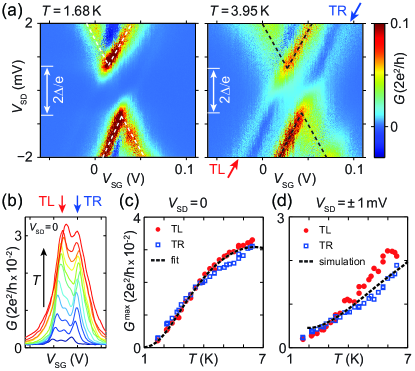
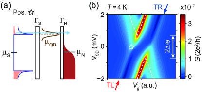
Figure 2(a) shows a detailed map of for a CB region of device A as function of and the gate voltage at K (left) and for an increased temperature of K (right). While we observe only the standard CB diamond edges separated by at the lowest , additional lines (arrows) labeled TL (left) and TR (right) appear for elevated temperatures besides the expected thermal broadening of CB features. At a finite bias , the conductance maxima of TL and TR are accompanied by regions of negative differential conductance (NDC, dark blue). We study the temperature dependence of these extra lines in cross-sections at and mV, shown for in the waterfall plot of Fig. 2(b). Each curve is an average over a small bias window in individual CB spectroscopy measurements using a moving average filter.Footnote:3 With increasing temperature the amplitude of the features TL and TR increase, while the background is zero due to CB.Footnote:4 To compare with the model below, we plot in Fig. 2(c) and (d) the temperature dependence of the maximum conductance of TL (red points) and TR (blue squares) for and mV, respectively, which show a qualitatively different, but distinctive monotonic increase in with increasing temperature. We ascribe the resonance lines TL and TR to the sequential tunneling of thermally excited QPs in the superconductor, as shown schematically in Fig. 3(a): at elevated temperatures of , the quasi-electron population at in S (light red) is finite. When the QD’s electrochemical potential is aligned with this population, i.e. , a current flows even for a bias smaller than , resulting in the additional resonance TL tuned by the bias and the gate voltages via the QD resonance condition. Similarly, the resonance TR is due to the condition for quasi-hole excitations.
We model these QP processes in a simple resonant tunneling picture.Levy Yeyati et al. (1997) If the bias is applied to S and we neglect superconducting correlations and the charge dynamics on the QD, the current can be approximated asLevy Yeyati et al. (1997); Gramich, Baumgartner, and Schönenberger (2015)
| (2) |
with the constant DOS in N and a BCS-type DOS in S normalized to the normal state, . are the Fermi functions in the respective contacts and is the BW transmission function of the QD, with , which also accounts for the gating of the QD by the gates (g, voltage ) and the contacts. The differential conductance can then be calculated directly. Figure 3(b) shows the resulting for meV, K, and . The model captures the gate voltage and bias dependence of the experiment very well, including the peak-dip structure with negative differential conductance (NDC) next to the TL/TR resonances due to the non-monotonic DOS of S. These results also agree with previous calculations using a microscopic model.Pfaller, Donarini, and Grifoni (2013)
To substantiate that the observed subgap features are due to thermal QP tunneling, we now analyze the temperature dependence of TL and TR’s resonance amplitudes at zero bias. The corresponding data are plotted in Fig. 2(c). For a zero-width QD resonance in Eq. 2, one finds at for . Thus, in agreement with a microscopic description,Gaass et al. (2014) we expect a low-temperature thermally activated characteristics of as and a decay at larger temperatures well known for sequential tunneling processes. Due to its large superconducting gap, device A is in the regime dominated by the term. To take into account both, the finite width of the resonance and the temperature dependence of ,Footnote:5 we fit Eq. 2 to the data using the BCS temperature dependence of the gap obtained from Eq. 1. Using meV and K determined independently, we obtain the tunnel couplings and as the only adjustable parameters for the best fit to the data. The fit is shown in Fig. 2(c) as a dashed line, which describes the data very accurately. The extracted coupling parameters agree well with the ones found from independent CB line shape fits in the normal state. This model also reproduces the finite-bias data: inserting the tunnel couplings obtained from the zero bias fit into Eq. 2, we obtain the mV amplitudes in a model simulation without additional fit parameters. The resulting curve is plotted as dashed line in Fig. 2(d) and also agrees well with the experiment. We note that for a given temperature, both, the experiment and the model exhibit only a very weak dependence of on for in the direction away from the CB diamond edge, see e.g. Fig. 2(a) and Fig. 3(b).
In conclusion, we demonstrate the growth and fabrication of an optimized Pd/Pb/In layer as narrow superconducting contact for carbon nanotube quantum dot devices, leading to reproducibly large and clean superconducting transport gaps. We illustrate ideal device characteristics, including a BCS-like temperature-dependence and a monotonic closing of the transport gap in magnetic fields. The large observed gaps allow us to identify subgap transport resonances as thermally activated quasiparticle tunneling. Their concise description by a simple resonant tunneling model corroborates a BCS-type density of states for the multi-layer contacts and provides an alternative possibility to determine the QD coupling strengths to the contacts. The implemented Pd coupling layer allows one to access different transport regimes with large and clean proximity gaps, a major advantage for the study of superconducting quantum dot hybrid structures.
This work was financially supported by the Swiss National Science Foundation (SNF), the Swiss Nanoscience Institute (SNI), the Swiss NCCR QSIT, the ERC project QUEST and the EU FP7 project SE2ND.
References
- Gräber et al. (2004) M. R. Gräber, T. Nussbaumer, W. Belzig, and C. Schönenberger, Nanotechnology 15, S479 (2004).
- Mourik et al. (2012) V. Mourik, K. Zuo, S. M. Frolov, S. R. Plissard, E. P. A. M. Bakkers, and L. P. Kouwenhoven, Science 336, 1003 (2012).
- Das Sarma, Freedman, and Nayak (2015) S. Das Sarma, M. Freedman, and C. Nayak, NPJ Quantum Information 1, 15001 (2015).
- Recher, Sukhorukov, and Loss (2001) P. Recher, E. V. Sukhorukov, and D. Loss, Phys. Rev. B 63, 165314 (2001).
- Hofstetter et al. (2009) L. Hofstetter, S. Csonka, J. Nygård, and C. Schönenberger, Nature 461, 960 (2009).
- Herrmann et al. (2010) L. G. Herrmann, F. Portier, P. Roche, A. Levy Yeyati, T. Kontos, and C. Strunk, Phys. Rev. Lett. 104, 026801 (2010).
- Schindele, Baumgartner, and Schönenberger (2012) J. Schindele, A. Baumgartner, and C. Schönenberger, Phys. Rev. Lett. 109, 157002 (2012).
- Das et al. (2012) A. Das, Y. Ronen, M. Heiblum, D. Mahalu, A. V. Kretinin, and H. Shtrikman, Nat. Commun. 3, 1165 (2012).
- Gramich, Baumgartner, and Schönenberger (2015) J. Gramich, A. Baumgartner, and C. Schönenberger, Phys. Rev. Lett. 115, 216801 (2015).
- Pillet et al. (2010) J.-D. Pillet, C. H. L. Quay, P. Morfin, C. Bena, A. Levy Yeyati, and P. Joyez, Nat. Phys. 6, 965 (2010).
- Dirks et al. (2011) T. Dirks, T. L. Hughes, S. Lal, B. Uchoa, Y.-F. Chen, C. Chialvo, P. M. Goldbart, and N. Mason, Nat. Phys. 7, 386 (2011).
- Lee et al. (2014) E. J. H. Lee, X. Jiang, M. Houzet, R. Aguado, C. M. Lieber, and S. De Franceschi, Nat. Nanotechn. 9, 79 (2014).
- Schindele et al. (2014) J. Schindele, A. Baumgartner, R. Maurand, M. Weiss, and C. Schönenberger, Phys. Rev. B 89, 045422 (2014).
- Bretheau et al. (2013) L. Bretheau, Ç. Ö. Girit, H. Pothier, D. Esteve, and C. Urbina, Nature 499, 312 (2013).
- Janvier et al. (2015) C. Janvier, L. Tosi, L. Bretheau, Ç. Ö. Girit, M. Stern, P. Bertet, P. Joyez, D. Vion, D. Esteve, M. F. Goffman, H. Pothier, and C. Urbina, Science 349, 1199 (2015).
- Gaass et al. (2014) M. Gaass, S. Pfaller, T. Geiger, A. Donarini, M. Grifoni, A. K. Hüttel, and C. Strunk, Phys. Rev. B 89, 241405 (2014).
- Ratz et al. (2014) S. Ratz, A. Donarini, D. Steininger, T. Geiger, A. Kumar, A. K. Hüttel, C. Strunk, and M. Grifoni, New J. Phys. 16, 123040 (2014).
- Higginbotham et al. (2015) A. P. Higginbotham, S. M. Albrecht, G. Kirs̆anskas, W. Chang, F. Kuemmeth, P. Krogstrup, T. S. Jespersen, J. Nygård, K. Flensberg, and C. M. Marcus, Nat. Phys. 11, 1017 (2015).
- Chang et al. (2015) W. Chang, S. M. Albrecht, T. S. Jespersen, F. Kuemmeth, P. Krogstrup, J. Nygård, and C. M. Marcus, Nat. Nanotechn. 10, 232 (2015).
- Taupin et al. (2016) M. Taupin, P. Krogstrup, H. Q. Nguyen, E. Mannila, S. M. Albrecht, J. Nygård, C. M. Marcus, and J. P. Pekola, arXiv:1601.01149 (2016).
- Grove-Rasmussen et al. (2009) K. Grove-Rasmussen, H. I. Jørgensen, B. M. Andersen, J. Paaske, T. S. Jespersen, J. Nygård, K. Flensberg, and P. E. Lindelof, Phys. Rev. B 79, 134518 (2009).
- Fülöp et al. (2015) G. Fülöp, F. Domínguez, S. d’Hollosy, A. Baumgartner, P. Makk, M. H. Madsen, V. A. Guzenko, J. Nygård, C. Schönenberger, A. Levy Yeyati, and S. Csonka, Phys. Rev. Lett. 115, 227003 (2015).
- Poole (2000) C. P. Poole, Handbook of Superconductivity, edited by C. P. Poole (Academic Press, San Diego, 2000).
- Chen et al. (2009) Y.-F. Chen, T. Dirks, G. Al-Zoubi, N. O. Birge, and N. Mason, Phys. Rev. Lett. 102, 036804 (2009).
- Bronn and Mason (2013) N. Bronn and N. Mason, Phys. Rev. B 88, 161409 (2013).
- Dirks et al. (2009) T. Dirks, Y.-F. Chen, N. O. Birge, and N. Mason, Appl. Phys. Lett. 95, 192103 (2009).
- Borzenets et al. (2015) I. V. Borzenets, Y. Shimazaki, G. F. Jones, M. F. Craciun, S. Russo, Y. Yamamoto, and S. Tarucha, arXiv:1506.04597 (2015).
- Whan and Orlando (1996) C. B. Whan and T. P. Orlando, Phys. Rev. B 54, R5255 (1996).
- Pfaller, Donarini, and Grifoni (2013) S. Pfaller, A. Donarini, and M. Grifoni, Phys. Rev. B 87, 155439 (2013).
- Skalski, Betbeder-Matibet, and Weiss (1964) S. Skalski, O. Betbeder-Matibet, and P. R. Weiss, Phys. Rev. 136, A1500 (1964).
- Yang et al. (2010) R. Yang, L. Zhang, Y. Wang, Z. Shi, D. Shi, H. Gao, E. Wang, and G. Zhang, Adv. Mat. 22, 4014 (2010).
- Samm et al. (2014) J. Samm, J. Gramich, A. Baumgartner, M. Weiss, and C. Schönenberger, J. Appl. Phys. 115, 174309 (2014).
- Eldridge, Van der Meulen, and Dong (1972) J. M. Eldridge, Y. J. Van der Meulen, and D. W. Dong, Thin Solid Films 12, 447 (1972).
- Kim et al. (2012) J. Kim, V. Chua, G. A. Fiete, H. Nam, A. H. MacDonald, and C.-K. Shih, Nat. Phys. 8, 464 (2012).
- Serrier-Garcia et al. (2013) L. Serrier-Garcia, J. C. Cuevas, T. Cren, C. Brun, V. Cherkez, F. Debontridder, D. Fokin, F. S. Bergeret, and D. Roditchev, Phys. Rev. Lett. 110, 157003 (2013).
- Levy Yeyati et al. (1997) A. Levy Yeyati, J. C. Cuevas, A. López-Dávalos, and A. Martín-Rodero, Phys. Rev. B 55, R6137 (1997).
- Thouless (1960) D. J. Thouless, Phys. Rev. 117, 1256 (1960).
- Douglass Jr. and Falicov (1964) D. H. Douglass Jr. and L. M. Falicov, in The Superconducting Energy Gap, Progress in Low Temperature Physics, Vol. 4, edited by C. Gorter (Elsevier, 1964) pp. 97 – 193.
- Gasparovic, Taylor, and Eck (1966) R. F. Gasparovic, B. N. Taylor, and R. E. Eck, Solid State Commun. 4, 59 (1966).
- (40) We use the Drude model to estimate the mean free path of our Pb strips from the measured low-temperature Pb strip resistivity. Assuming the bulk literature values of PbPoole (2000) for the coherence length nm and the penetration depth nm in the clean limit (), we estimate the coherence length and penetration depth of our Pb strips using the interpolation formulae suitable for the regime , and , Tinkham (2004) respectively.
- (41) We use the equations and of Ref. 30, valid in the dirty limit and for , to calculate the dependence of the visible transport gap (the spectral quasiparticle gap) as a function of . Here, is the order parameter, the experimentally determined transport gap at and at base temperature, and the pair-breaking parameter with the exponent .Skalski, Betbeder-Matibet, and Weiss (1964); Tinkham (2004) Note that we use as adjustable parameter so that vanishes at the experimentally determined values.
- Tinkham (2004) M. Tinkham, Introduction to Superconductivity, 2nd ed. (Dover, 2004).
- (43) We ascribe the small central subgap conductance peak between TL and TR to the thermally broadenend DOS in the S contact, coinciding with . The analysis at mV shows that this finite subgap conductance at elevated temperatures has no influence on our analysis.
- (44) We carefully controlled that no structures are lost or created in the averaging procedure.
- (45) In the studied temperature range , the closing of the transport gap for plays already a significant role.