Present address: ]High Field Magnet Laboratory (HFML-EMFL), Institute for Molecules and Materials, Radboud University, Toernooiveld 7, 6525 ED Nijmegen, The Netherlands
Excitons in atomically thin black phosphorus
Abstract
Raman scattering and photoluminescence spectroscopy are used to investigate the optical properties of single layer black phosphorus obtained by mechanical exfoliation of bulk crystals under an argon atmosphere. The Raman spectroscopy, performed in situ on the same flake as the photoluminescence measurements, demonstrates the single layer character of the investigated samples. The emission spectra, dominated by excitonic effects, display the expected in plane anisotropy. The emission energy depends on the type of substrate on which the flake is placed due to the different dielectric screening. Finally, the blue shift of the emission with increasing temperature is well described using a two oscillator model for the temperature dependence of the band gap.
Black phosphorus, the most stable of all the allotropes of phosphorus, has been intensively studied by different experimental methods from the early fifties of the last century.Keyes (1953); Warschauer (1963); Maruyama et al. (1981); Asahina et al. (1983); Jamieson (1963); Wittig and Matthias (1968); Sugai and Shirotani (1985) Bulk black phosphorus is a semiconductor, with a band gap of about .Keyes (1953); Asahina et al. (1983) The orthorombic bulk crystal has a layered structure, with atomic layers bound by weak van der Waals interactions. A single atomic layer is puckered, with the phosphorus atoms being parallel in the (010) plane.Narita et al. (1983); Takao et al. (1981); Maruyama et al. (1981) Atomically thin monolayers have been recently isolated using mechanical exfoliation,Castellanos-Gomez et al. (2014) adding black phosphorus to the rapidly growing family of emerging two dimensional materials. The band gap of black phosphorus is always direct and can be tuned from to the nearly visible part of the spectrumTran et al. (2014); Ling et al. (2015). In contrast, graphene is gapless,Novoselov et al. (2005) and the transition metals dichalcogenides (TMDs) have an indirect gap in bulk phase and only monolayer TMDs have a direct gap.Wang et al. (2012) Moreover, black phosphorus exhibits a strong in-plane anisotropyTran et al. (2014); Low et al. (2014); Xia et al. (2014); Qiao et al. (2014); Ling et al. (2015), absent in graphene and TMDs. Additionally, the relatively high mobilities measured at room temperature combined with the direct band gap result in an on/off ratio for FET transistors of the order of 105. Ling et al. (2015); Li et al. (2014); Liu et al. (2014)
Although black phosphorus has a wide range of possible applications, including tunable photodetectorsBuscema et al. (2014), field effect transistorsXia et al. (2014); Ling et al. (2015); Li et al. (2014); Liu et al. (2014) or photon polarizersTran et al. (2014); Low et al. (2014); Xia et al. (2014); Qiao et al. (2014); Ling et al. (2015), many of its electronic properties are not yet fully understood. The main difficulty arises from the sensitivity of black phosphorus to its environment, notably its high reactivity when exposed to air and laser light.Castellanos-Gomez et al. (2014); Koenig et al. (2014); Gan et al. (2015) Theoretical calculations predict a band gap of monolayer black phosphorus ranging from Liu et al. (2014); Tran et al. (2014) to Castellanos-Gomez et al. (2014); Tran et al. (2014), with a binding energy of the neutral exciton of in vacuum Tran et al. (2014) and of when placed on a SiO2 substrate Castellanos-Gomez et al. (2014). The measured photoluminescence (PL) emission energy from bilayers black phosphorus is between Zhang et al. (2014) and Castellanos-Gomez et al. (2014), while monolayer black phosphorus shows neutral exciton emission around Wang et al. (2015), Liu et al. (2014) or Yang et al. (2015). The latter value was related to the simultaneous observation of charged exciton emission at around .Yang et al. (2015) Using scanning tunneling microscopy the band gap of a single layer of black phosphorus was estimated to be .Liang et al. (2014) The exciton binding energy and consequently the emission energy strongly depend on the dielectric environment (substrate) Castellanos-Gomez et al. (2014); Woomer et al. (2015). This could partially explain the wide range of values for the black phosphorus emission energy found in the literature, possibly related also to a slightly different composition of the SiO2 substrates employed. Moreover, owing to the limited life time of the samples, the various characterization techniques used to identify monolayer black phosphorus (e.g. atomic force microscopy, Raman spectroscopy) could not always be performed on the same flake where the optical response was investigated.
In this paper we present a systematic investigation of the optical properties of monolayers of black phosphorus. We analyze the properties of the emission as a function of the dielectric constant of the substrate, excitation power, polarization and temperature. The single layer character of the investigated flakes is demonstrated using in situ Raman measurements on the same flake used for the PL. We show that the PL emission energy of monolayer black phosphorus depends on the substrate used. The PL spectra, dominated by excitonic effects, exhibit the expected in plane anisotropy. Finally, the blue shift of the emission energy with an increasing temperature is well described with a two-oscillator model for the temperature dependence of the band gap.
Single and few layer black phosphorus flakes have been obtained by mechanical exfoliation of a bulk crystal, purchased from Smart Elements (99.998% nominal purity). The mechanical exfoliation was performed in a glove box filled with argon (Ar) gas ( O2, H2O). The flakes were subsequently transferred onto a Si substrate, in most cases capped with a thick layer of SiO2 (Si/SiO2 hereafter). The samples were stored in vials, in the glove box, before their transfer to the cryostat under an Ar atmosphere.
For the optical measurements, the samples were mounted on the cold finger of a He-flow cryostat, which was then rapidly pumped to a pressure below , minimizing the exposure of the black phosphorus to air. The excitation was provided by a frequency-doubled diode laser, emitting at and focused on the sample by a 50 microscope objective (0.55 numerical aperture), yielding a spot size of . The PL and Raman signals were collected through the same objective and analyzed by a spectrometer equipped with a liquid nitrogen cooled Si CCD camera.
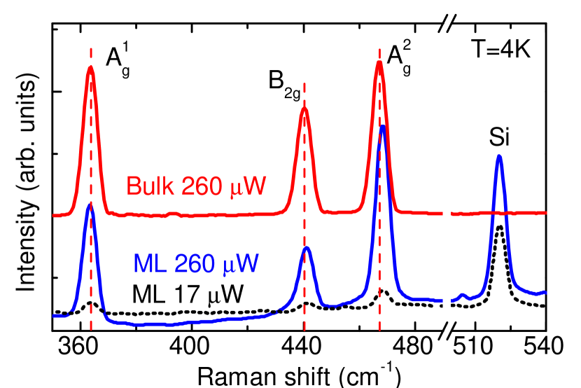
Raman spectroscopy, which has been shown to be a very precise tool for the determination of the number of layers in TMDs Lee et al. (2010); Guti rrez et al. (2013); Li et al. (2012a, b); Wang et al. (2012) and in graphene, Ferrari et al. (2006); Gupta et al. (2006) can also be used to identify monolayer black phosphorus. Bulk black phosphorus belongs to the space group. Of the 12 normal modes at the point of the Brillouin zone, six are Raman active.Sugai et al. (1981); Sugai and Shirotani (1985) The two B3g modes are forbidden in back scattering configuration and the B1g mode at is very weak. Therefore, only three Raman modes are expected for bulk black phosphorus: A, A and B2g at around , and , respectively.Sugai et al. (1981); Sugai and Shirotani (1985) The A and B2g modes are related to the in plane vibrations of the atoms, while A mode is related to the out of plane movement of the atoms Sugai et al. (1981); Sugai and Shirotani (1985).
Typical calibrated micro Raman (Raman) spectra of the bulk and single layer black phosphorus are presented in Fig. 1. For the bulk crystal three strong peaks are observed at , and corresponding well to the expected main Raman modes. A further peak was systematically observed at (Raman mode of the Si substrate), confirming the correct calibration of our Raman setup. The slight shift towards lower frequencies, compared to the previously cited literature values, can be related to the low temperature () at which our measurements have been carried out.Zhang et al. (2014) Under low excitation power (), initially used to avoid any risk of inducing damage by exposure to the laser light, the Raman spectrum of the monolayer flake is similar to that of the bulk crystal. This suggests that the monolayer black phosphorus remains crystalline and no oxidization occurred during the transfer of the sample from the glove box to the cryostat. Compared to bulk, the A mode does not shift within experimental error. Although this Raman mode was found to soften in a monolayer sample Liu et al. (2014), it was generally found to be rather insensitive to the number of layers.Favron et al. (2015); Lu et al. (2014) In contrast, the position of A and B2g Raman modes shift to higher frequencies in the monolayer flake. The A mode shifts by while the B2g shifts by 1.0. The change of the energy of the Raman modes as a function of the number of layers in black phosphorus has been already shown for both high Favron et al. (2015); Castellanos-Gomez et al. (2014); Liu et al. (2014) and low frequency modes Luo et al. (2015). The shifts we measure are in good agreement with the reported values for single layer black phosphorus ( and around for A Favron et al. (2015); Castellanos-Gomez et al. (2014); Liu et al. (2014); Lu et al. (2014) and B2g Favron et al. (2015); Castellanos-Gomez et al. (2014), respectively) demonstrating the single layer character of the investigated flake. Raman measured at high excitation power (, the same as used for the bulk crystal) does not show any additional features; the peak positions remain the same as for the data obtained for low excitation power. Thus there is no sign of laser induced chemical modification of our samples,Castellanos-Gomez et al. (2014) which is important since the excitation intensity used here is comparable to that used in our micro PL (PL) spectroscopy measurements.
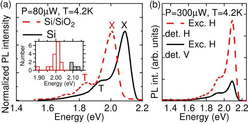
In Fig. 2(a) we show representative low temperature PL spectra for the monolayer flake previously characterized using Raman spectroscopy. The measurement was performed without removing the flake from the cryostat, which was maintained under vacuum. The spectrum is dominated by a very strong emission line centered at around identified with neutral exciton recombination. This line is consistently observed at this energy for all flakes transferred to Si/SiO2 substrates. The typical full width at half maximum is of (line broadening induced by scattering with vacancies and impurities in the exfoliated flakes). The observed value of the exciton recombination energy is relatively high as compared to the theoretical band gap of eV computed for black phosphorus single layer,Castellanos-Gomez et al. (2014); Tran et al. (2014) suggesting that the investigated sample is indeed a single layer. This is somewhat larger than the values already reported for black phosphorus single layers of Liu et al. (2014); Yang et al. (2015); Wang et al. (2015). This could be partly ascribed to the different stoichiometry of the SiO2 layers used as a substrate, which induces a shift in the emission because of the different dielectric constant of the surrounding medium.Choi and Strano (2007) To verify this hypothesis, we have transferred black phosphorus flakes onto a Si substrate covered by a thin () layer of native oxide. Such a substrate has a larger dielectric constant than the standard Si/SiO2 substrates. Thus, the exciton binding energy is expected to be lower and the emission energy should be blue shifted. A typical PL spectrum of a flake transferred onto a Si substrate is shown in Fig. 2(a). While the main spectral features resemble those of a flake on a Si/SiO2 substrate, there is a large shift of the emission energy of . This confirms the dependence of the emission energy on the dielectric environment, in agreement with previous results.Castellanos-Gomez et al. (2014); Woomer et al. (2015) The effect of the dielectric environment seems to be stronger than for atomically thin TMDs, in agreement with theory and experiment.Lin et al. (2014) However, we note that the effect of the dielectric environment alone is too small to account for the large variation of the emission energy reported in the literature.Liu et al. (2014); Yang et al. (2015); Wang et al. (2015)
In the spectrum measured on a Si/SiO2 substrate, in addition to the neutral exciton recombination, we observed additional features at , which can be attributed to charged exciton recombination (systematically present in all the investigated flakes)Yang et al. (2015) together with a low energy peak, typically at , and possibly related to excitons bound to impurities. The low energy feature is not always present, see e.g. the PL spectrum on a Si substrate in Fig. 2(a).
Because of the low symmetry of the crystal structure and the screening in black phosphorus Tran et al. (2014); Li and Appelbaum (2014), the exciton wave function is expected to be squeezed along the armchair direction, resulting in a polarization dependent PL emission Wang et al. (2015). The linear polarization dependence of the emission of our flakes was investigated by mounting polarizers/analyzers in both the excitation and the detection paths. For any fixed orientation of the analyzer in the detection path, the detected signal is always stronger for horizontally (H) polarized excitation. This stems from the polarization dependent absorption properties of black phosphorus Xia et al. (2014). Regardless of the polarization of the excitation beam, whenever the analyzer in the detection path was set to H, the intensity of the detected signal was a maximum, which is consistent with the strongly anisotropic nature of the exciton in black phosphorus Wang et al. (2015). For example, in Fig. 2(b), we show PL spectra excited with a H polarized laser light and detected with either H or vertical (V) direction of the analyzer.
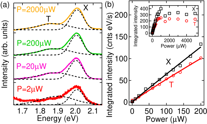
The evolution of the PL spectra as a function of the excitation power gives information concerning the nature of the observed transition lines. We have measured the power dependence of the PL spectra for several black phosphorus monolayer flakes. In Fig. 3(a) we show representative spectra measured at low, intermediate, and high excitation powers at . Even after exciting with , the emission efficiency did not decrease for any of the investigated samples, suggesting that our preparation method helps improve the stability of the exfoliated black phosphorus flakes. Two peaks appear in the spectra of Fig. 3(a) for all excitation powers used. The neutral exciton peak slightly blue shifts () at high excitation powers, possibly due to a localized heating effect induced by the high power of the incoming laser beam (see also below for a discussion of temperature dependence of the black phosphorus PL).
In Fig. 3(b) we present the dependence of the integrated PL intensity of neutral and charged excitons as a function of the excitation power. At low excitation power, both intensities increase linearly with the power (indicating the absence of biexciton emission), as demonstrated by the fits to the power law , with for the neutral exciton and for the charged exciton. At higher excitation power, both excitonic lines saturate at approximately the same level of excitation power [, see insert to Fig. 3(b)], confirming that the two observed transitions are related to the recombination of a single electron-hole pair.
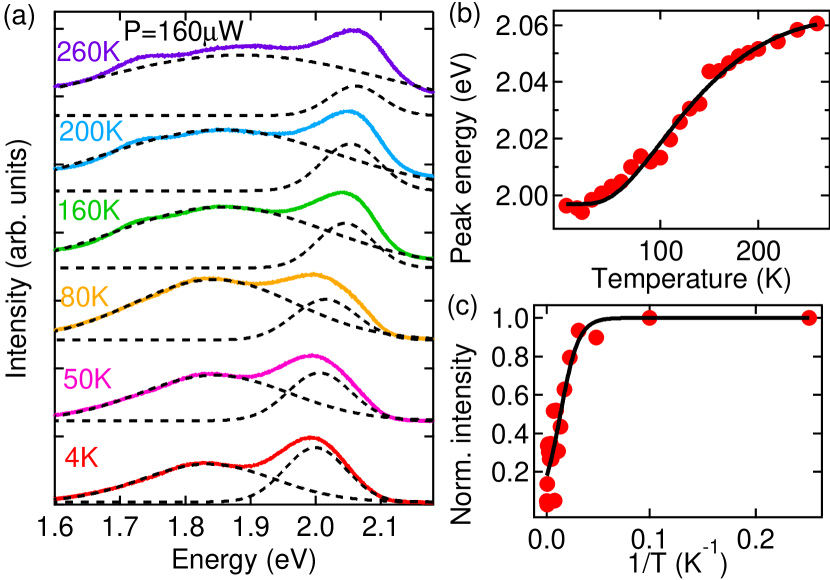
In view of the potential use of black phosphorus in a wide variety of electronic and optoelectronic applications, we have investigated the temperature dependence of its optical properties. In Fig. 4(a) we show normalized PL spectra measured at different temperatures. With increasing temperature the charged exciton peak broadens. The neutral exciton emission blue shifts (measured between and ), which is consistent with earlier reports of the temperature dependence of the band gap of bulk black phosphorus ( Warschauer (1963) or Baba et al. (1991)). The behavior of the emission energy of the excitonic peak is shown more in detail in Fig. 4(b). In bulk semiconductors, the variation of the band gap as a function of the temperature is direct consequence of the renormalization of the band gap via the electron-phonon interaction and of the thermal expansion of the lattice.Cardona and Thewalt (2005) In the framework of the two-oscillator modelViña et al. (1984); Cardona and Kremer (2014); Dey et al. (2013); Lian et al. (2006), the band gap is approximated by
where is the bare band gap (i.e. the low temperature band gap exhibited in the absence of zero point motion), is the renormalization energy and and denote the two oscillator energies, as extracted from the computed phonon density of states of monolayer black phosphorus.Aierken et al. (2015) The neutral exciton emission energy is then given by , where is the exciton binding energy. The solid curve shown in Fig. 4(b) is obtained by fitting the experimental data, yielding (larger than the observed low transition energy, suggesting the occurrence of band gap renormalization due to electron-phonon interaction), , and .
The integrated intensity of the excitonic transition as a function of the inverse substrate temperature is shown in Fig. 4(c). With increasing temperature, the emission intensity decreases, owing to the thermal activation of non-radiative recombination centers. To quantify the activation energy , the experimental data is fitted using ,Leroux et al. (1999) where is related to the ratio of the radiative and non-radiative lifetimes,Fang et al. (2015) to give , and . The significantly lower value of as compared to the computed exciton binding energy Castellanos-Gomez et al. (2014) confirms that the decrease of the PL intensity at high is brought about by the thermal occupation of non radiative recombination centers rather than the dissociation of the excitons.
In summary, we have performed a detailed investigation of the optical properties of monolayer black phosphorus mechanically exfoliated in an Ar atmosphere. No significant degradation of the PL emission was induced by the laser illumination, suggesting that this preparation method preserves the optical properties of the black phosphorus flakes. The shift of the Raman modes measured on the exfoliated flakes with respect to the bulk black phosphorus confirms the single layer character of the exfoliated black phosphorus flakes. The measured PL spectra exhibit strong emission lines, attributed to the recombination of neutral and charged excitonic complexes. It is not clear if the enhanced emission energy, compared to the previously reported values,Liu et al. (2014); Yang et al. (2015); Wang et al. (2015) is linked with a larger intrinsic band gap or a reduced exciton binding energy. The excitonic nature of the observed PL was confirmed by the observed polarization dependence and by the nearly linear increase of the emission intensity with the excitation power. The increase in the emission energy with temperature was modeled with a two-oscillator model to account for the temperature dependence of semiconductor band gap.
Acknowledgements.
The authors gratefully acknowledge Baptiste Vignolle for his assistance with the glove box and for his careful proof reading and Geert Rikken for providing the bulk black phosphorus. AAM acknowledges financial support from the French foreign ministry. This work was partially supported by ANR JCJC project milliPICS, the Région Midi-Pyrénées under contract MESR 13053031 and STCU project 5809.References
- Keyes (1953) R. W. Keyes, Physical Review 92, 580 (1953).
- Warschauer (1963) D. Warschauer, Journal of Applied Physics 34, 1853 (1963).
- Maruyama et al. (1981) Y. Maruyama, S. Suzuki, K. Kobayashi, and S. Tanuma, Physica B+C 105, 99 (1981).
- Asahina et al. (1983) H. Asahina, Y. Maruyama, and A. Morita, Physica B+C 117 118, Part 1, 419 (1983).
- Jamieson (1963) J. C. Jamieson, Science 139, 1291 (1963).
- Wittig and Matthias (1968) J. Wittig and B. T. Matthias, Science 160, 994 (1968).
- Sugai and Shirotani (1985) S. Sugai and I. Shirotani, Solid State Communications 53, 753 (1985).
- Narita et al. (1983) S. Narita, S. Terada, S. Mori, K. Muro, Y. Akahama, and S. Endo, Journal of the Physical Society of Japan 52, 3544 (1983).
- Takao et al. (1981) Y. Takao, H. Asahina, and A. Morita, Journal of the Physical Society of Japan 50, 3362 (1981).
- Castellanos-Gomez et al. (2014) A. Castellanos-Gomez, L. Vicarelli, E. Prada, J. O. Island, K. L. Narasimha-Acharya, S. I. Blanter, D. J. Groenendijk, M. Buscema, G. A. Steele, J. V. Alvarez, H. W. Zandbergen, J. J. Palacios, and H. S. J. van der Zant, 2D Materials 1, 025001 (2014).
- Tran et al. (2014) V. Tran, R. Soklaski, Y. Liang, and L. Yang, Physical Review B 89, 235319 (2014).
- Ling et al. (2015) X. Ling, H. Wang, S. Huang, F. Xia, and M. S. Dresselhaus, Proceedings of the National Academy of Sciences 112, 4523 (2015).
- Novoselov et al. (2005) K. S. Novoselov, A. K. Geim, S. V. Morozow, D. Jiang, M. I. Katsnelson, I. V. Grigorieva, S. V. Dubonos, and A. A. Firsov, Nature 438, 197 (2005).
- Wang et al. (2012) Q. H. Wang, K. Kalantar-Zadeh, A. Kis, J. N. Coleman, and M. S. Strano, Nature Nanotechnology 7, 699 (2012).
- Low et al. (2014) T. Low, A. S. Rodin, A. Carvalho, Y. Jiang, H. Wang, F. Xia, and A. H. Castro Neto, Physical Review B 90, 075434 (2014).
- Xia et al. (2014) F. Xia, H. Wang, and Y. Jia, Nature Communications 5, 4458 (2014).
- Qiao et al. (2014) J. Qiao, X. Kong, Z.-X. Hu, F. Yang, and W. Ji, Nature Communications 5, 4475 (2014).
- Li et al. (2014) L. Li, Y. Yu, G. J. Ye, Q. Ge, X. Ou, H. Wu, D. Feng, X. H. Chen, and Y. Zhang, Nature Nanotechnology 9, 372 (2014).
- Liu et al. (2014) H. Liu, A. T. Neal, Z. Zhu, Z. Luo, X. Xu, D. Tománek, and P. D. Ye, ACS Nano 8, 4033 (2014).
- Buscema et al. (2014) M. Buscema, D. J. Groenendijk, S. I. Blanter, G. A. Steele, H. S. J. van der Zant, and A. Castellanos-Gomez, Nano Letters 14, 3347 (2014).
- Koenig et al. (2014) S. P. Koenig, R. A. Doganov, H. Schmidt, A. H. Castro Neto, and B. Özyilmaz, Applied Physics Letters 104, 103106 (2014).
- Gan et al. (2015) Z. X. Gan, L. L. Sun, X. L. Wu, M. Meng, J. C. Shen, and P. K. Chu, Applied Physics Letters 107, 021901 (2015).
- Zhang et al. (2014) S. Zhang, J. Yang, R. Xu, F. Wang, W. Li, M. Ghufran, Y.-W. Zhang, Z. Yu, G. Zhang, Q. Qin, and Y. Lu, ACS Nano 8, 9590 (2014).
- Wang et al. (2015) X. Wang, A. M. Jones, K. L. Seyler, V. Tran, Y. Jia, H. Zhao, H. Wang, L. Yang, X. Xu, and F. Xia, Nature Nanotechnology 10, 517 (2015).
- Yang et al. (2015) J. Yang, R. Xu, J. Pei, Y. W. Myint, F. Wang, Z. Wang, S. Zhang, Z. Yu, and Y. Lu, Light-Science & Applications 4, e312 (2015).
- Liang et al. (2014) L. Liang, J. Wang, W. Lin, B. G. Sumpter, V. Meunier, and M. Pan, Nano Letters 14, 6400 (2014).
- Woomer et al. (2015) A. H. Woomer, T. W. Farnsworth, J. Hu, R. A. Wells, C. L. Donley, and S. C. Warren, ACS Nano 9, 8869 (2015).
- Lee et al. (2010) C. Lee, H. Yan, L. E. Brus, T. F. Heinz, J. Hone, and S. Ryu, ACS Nano 4, 2695 (2010).
- Guti rrez et al. (2013) H. R. Guti rrez, N. Perea-L pez, A. L. El as, A. Berkdemir, B. Wang, R. Lv, F. L pez-Ur as, V. H. Crespi, H. Terrones, and M. Terrones, Nano Letters 13, 3447 (2013).
- Li et al. (2012a) H. Li, Q. Zhang, C. C. R. Yap, B. K. Tay, T. H. T. Edwin, A. Olivier, and D. Baillargeat, Advanced Functional Materials 22, 1385 (2012a).
- Li et al. (2012b) S.-L. Li, H. Miyazaki, H. Song, H. Kuramochi, S. Nakaharai, and K. Tsukagoshi, ACS Nano 6, 7381 (2012b).
- Ferrari et al. (2006) A. C. Ferrari, J. C. Meyer, V. Scardaci, C. Casiraghi, M. Lazzeri, F. Mauri, S. Piscanec, D. Jiang, K. S. Novoselov, S. Roth, and A. K. Geim, Physical Review Letters 97, 187401 (2006).
- Gupta et al. (2006) A. Gupta, G. Chen, P. Joshi, S. Tadigadapa, and Eklund, Nano Letters 6, 2667 (2006).
- Sugai et al. (1981) S. Sugai, T. Ueda, and K. Murase, Journal of the Physical Society of Japan 50, 3356 (1981).
- Favron et al. (2015) A. Favron, E. Gaufres, F. Fossard, A.-L. Phaneuf-L’Heureux, N. Y.-W. Tang, P. L. Levesque, A. Loiseau, R. Leonelli, S. Francoeur, and R. Martel, Nature Materials 14, 826 (2015).
- Lu et al. (2014) W. Lu, H. Nan, J. Hong, Y. Chen, C. Zhu, Z. Liang, X. Ma, Z. Ni, C. Jin, and Z. Zhang, Nano Research 7, 853 (2014).
- Luo et al. (2015) X. Luo, X. Lu, G. K. W. Koon, A. H. C. Neto, B. Özyilmaz, Q. Xiong, and S. Y. Quek, Nano Letters 15, 3931 (2015).
- Choi and Strano (2007) J. H. Choi and M. S. Strano, Applied Physics Letters 90, 3114 (2007).
- Lin et al. (2014) Y. Lin, X. Ling, L. Yu, S. Huang, A. L. Hsu, Y.-H. Lee, J. Kong, M. S. Dresselhaus, and T. Palacios, Nano Letters 14, 5569 (2014).
- Li and Appelbaum (2014) P. Li and I. Appelbaum, Physical Review B 90, 115439 (2014).
- Baba et al. (1991) M. Baba, Y. Nakamura, K. Shibata, and A. Morita, Japanese Journal of Applied Physics 30, L1178 (1991).
- Cardona and Thewalt (2005) M. Cardona and M. L. W. Thewalt, Reviews of Modern Physics 77, 1173 (2005).
- Viña et al. (1984) L. Viña, S. Logothetidis, and M. Cardona, Physical Review B 30, 1979 (1984).
- Cardona and Kremer (2014) M. Cardona and R. K. Kremer, Thin Solid Films 571, 680 (2014).
- Dey et al. (2013) P. Dey, J. Paul, J. Bylsma, D. Karaiskaj, J. M. Luther, M. C. Beard, and A. H. Romero, Solid State Communications 165, 49 (2013).
- Lian et al. (2006) H. J. Lian, A. Yang, M. L. W. Thewalt, R. Lauck, and M. Cardona, Physical Review B 73, 233202 (2006).
- Aierken et al. (2015) Y. Aierken, D. Çakır, C. Sevik, and F. M. Peeters, Physical Review B 92, 081408 (2015).
- Leroux et al. (1999) M. Leroux, N. Grandjean, B. Beaumont, G. Nataf, F. Semond, J. Massies, and P. Gibart, Journal of Applied Physics 86, 3721 (1999).
- Fang et al. (2015) Y. Fang, L. Wang, Q. Sun, T. Lu, Z. Deng, Z. Ma, Y. Jiang, H. Jia, W. Wang, J. Zhou, and H. Chen, Scientific Reports 5, 12718 (2015).