Crystal-phase quantum dots in GaN quantum wires
Abstract
We study the nature of excitons bound to I1 basal plane stacking faults in ensembles of ultrathin GaN nanowires by continuous-wave and time-resolved photoluminescence spectroscopy. These ultrathin nanowires, obtained by the thermal decomposition of spontaneously formed GaN nanowire ensembles, are tapered and have tip diameters down to 6 nm. With decreasing nanowire diameter, we observe a strong blue shift of the transition originating from the radiative decay of stacking fault-bound excitons. Moreover, the radiative lifetime of this transition in the ultrathin nanowires is independent of temperature up to 60 K and significantly longer than that of the corresponding transition in as-grown nanowires. These findings reveal a zero-dimensional character of the confined exciton state and thus demonstrate that I1 stacking faults in ultrathin nanowires act as genuine quantum dots.
Spontaneously formed GaN nanowires are comparable in structural perfection to state-of-the-art freestanding GaN.Zettler et al. (2015) The nanowire geometry inhibits the propagation of threading dislocations along the nanowire axis, resulting in dislocation-free crystals regardless of the substrate.Hersee et al. (2011); Kishino and Ishizawa (2015) In contrast to group-III arsenide and phosphide nanowires, which are synthesized by vapor-liquid-solid growth and are prone to a pronounced polytypism,Bao et al. (2008); Corfdir et al. (2013) spontaneously formed GaN nanowires exclusively crystallize in the wurtzite lattice structure with only occasional I1 basal plane stacking faults (BSFs).Calleja et al. (2007); Geelhaar et al. (2011) Consequently, the radiative transitions related to excitons bound to I1 BSFs [] in GaN nanowires are spectrally well resolved and distinct from other excitonic transitions in GaN. This fact has been essential for shedding light on the nature of the .Corfdir et al. (2014); Korona et al. (2014) In particular, for nanowires with a diameter larger than 50 nm, the was shown to exhibit a two-dimensional density of states, i. e., I1 BSFs indeed act as quantum wells.Stampfl and Van de Walle (1998); Corfdir et al. (2014)
These so-called crystal-phase quantum structures are free of strain and alloy disorder, their interfaces are atomically abrupt.Akopian et al. (2010) In GaN nanowires, the decay of the is purely radiative up to 60 K.Corfdir et al. (2014); Korona et al. (2014) BSFs thus form an exceptionally well-defined model system for fundamental studies of confined excitons. In this context, the recent fabrication of ultrathin GaN nanowires with a diameter down to 6 nm is of great interest.Zettler et al. (2016) Due to the mismatch in dielectric constants between GaN and air, excitons in these ultrathin nanowires experience a strong radial confinement, i. e., the ultrathin GaN nanowires act as quantum wires despite the fact that their diameter still exceeds at least twice the exciton Bohr radius.Zettler et al. (2016) In addition, the thermal decomposition technique used for the controlled thinning of the as-grown nanowires does not affect their high structural perfection. Finally, despite their extremely small diameter, these nanostructures exhibit a high radiative efficiency due to a rather slow surface recombination velocity at the nanowires’ sidewall facets less than than 210 cm/s at 60 K.Corfdir et al. (2014)
In this work, we use continuous-wave (cw) and time-resolved (TR) photoluminescence (PL) spectroscopy to investigate the radiative decay and the dynamics of the in GaN quantum wire ensembles fabricated by partial thermal decomposition. We demonstrate that I1 BSFs in these nanowires act as quantum dots. With decreasing nanowire diameter, the transition blueshifts as a result of radial confinement. The radiative lifetime of the in crystal-phase quantum dots does not vary with temperature and is significantly longer than the one measured at 5 K for as-grown nanowires. Using self-consistent eight-band calculations, we show that the increase in radiative lifetime with decreasing diameter results from the reduced coherence area of the .
Ultrathin GaN nanowires with a length of about 1 µm have been obtained by partial thermal decomposition at 920 °C of GaN nanowire ensembles formed during molecular beam epitaxy on a Si(111) substrate.Zettler et al. (2016) The length and the diameter of the as-grown nanowires are 2 µm and 51 nm, respectively, and we estimate the density of I1 BSFs to be about 1 per nanowire (see the cathodoluminescence mappings in Ref. Corfdir et al., 2014). The concurrent layer-by-layer desorption of atoms from the top surface and from the sidewalls leads to tapering. The thinnest nanowires obtained exhibit an average base diameter nm while the diameter at their tip can be as small as 6 nm.Zettler et al. (2016) Following the results in Ref. Zettler et al., 2016, ultrathin nanowires are referred to as quantum wires in the remainder of the paper. Charging effects leads to an overestimation of the tip diameters when measuring such thin wires by top-view and cross-sectional secondary electron microscopy.Zettler et al. (2016); Loitsch et al. (2015) Therefore, the emission properties of GaN quantum wires were correlated with their average . Note, however, that the emission is very likely to originate from sections of the nanowires with diameter substantially smaller than .
Continuous-wave (cw) PL experiments were performed using the 325 nm line of a HeCd laser for excitation. The laser was focused onto the sample to a diameter of 60 µm. The PL signal was analyzed using a monochromator followed by a charge-coupled device camera for detection. Time-resolved (TR) PL spectroscopy was carried out using the second harmonic of fs pulses obtained from an optical parametric oscillator pumped by a Ti:sapphire laser (emission wavelength and repetition rate of 325 nm and 76 MHz, respectively). The energy fluence per pulse was kept below 0.3 µJ/cm2. The transient emission was spectrally dispersed by a monochromator and detected by a streak camera operating in single shot mode. For both cw and TR PL measurements, the samples were mounted in a coldfinger cryostat whose temperature can be varied between 5 and 300 K. For both experiments, the laser was polarized perpendicular to the nanowire axis. As the average nanowire diameter for all of samples is well within the sub-wavelength range, the coupling of light into the nanowires is getting less and less efficient with decreasing diameter, thus strongly reducing absorption. The photogenerated carrier density in the quantum wires should thus be lower as compared to the as-grown nanowires.
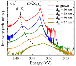
Figure 1 shows the PL spectra at 5 K for an ensemble of as-grown nanowires and for ensembles of partially decomposed, quantum wires with between 39 and 27 nm. The spectrum for the as-grown ensemble is dominated by the recombination of A excitons bound to neutral O donors at 3.471 eV []. The lower energy band centered at 3.410 eV is related to the recombination of excitons bound to I1 BSFs.Corfdir et al. (2014); Korona et al. (2014)
Decreasing from 51 to 27 nm, the energy of the transition increases from 3.471 to 3.481 eV (Fig. 1), indicating a progressively stronger confinement of the excitons in the corresponding nanowires. This confinement is caused by the mismatch in dielectric constants between GaN and vacuum at the nanowire sidewalls.Keldysh (1979); Kumagai and Takagahara (1989); Zettler et al. (2016) An even stronger blueshift (42 meV) with decreasing nanowire diameter is observed for the line, suggesting that the state in GaN quantum wires is radially confined. In other words, BSFs in GaN quantum wires seem to act as crystal-phase quantum dots. The larger blueshift of the as compared to the one observed for the line probably arises from the different location of the exciton states involved in these transitions: whereas donors are distributed uniformly along the entire length of the nanowire, I1 BSFs may be located preferentially in the top parts of the nanowires, where the diameter is smaller and the confinement of the exciton stronger. This result is consistent with the fact that BSFs result from the nanowire coalescence and form several hundreds of nm above the contact point between adjacent nanowires.Consonni et al. (2009) We also observe that the thinnest nanowires exhibit the broadest and lines at 5 K (Fig. 1). This finding is a direct consequence of the increase in confinement with decreasing diameter: the thinner the nanowire, the larger the impact of diameter fluctuations on the and energies and hence the larger the broadening of the corresponding emission lines. As a result of the significant spectral overlap between the and transitions for the thinnest nanowires (Fig. 1), we focus in the following on the optical properties of the quantum wires with and 32 nm.
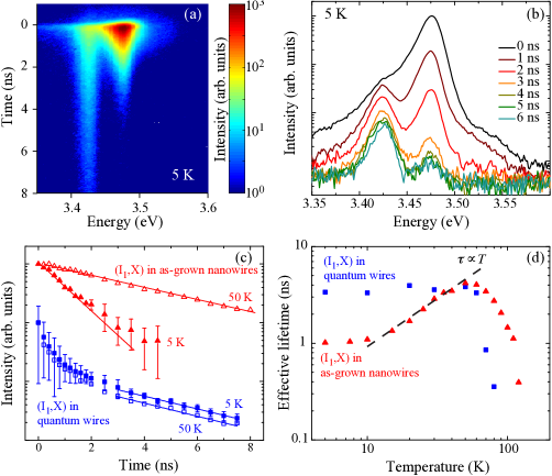
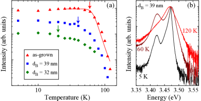
Figure 2(a) shows the temperature dependence of the integrated intensity of the line for the as-grown nanowire ensembles and for two quantum wire ensembles with and 32 nm. For the as-grown nanowire ensemble, the intensity of the transition remains constant between 4 and 60 K, indicating that the recombination of the is purely radiative up to 60 K.Corfdir et al. (2014) For temperatures above 60 K, excitons can thermally escape from the comparatively shallow crystal-phase quantum well, leading to an abrupt quenching of the line.Graham et al. (2013); Rudolph et al. (2013) The intensity of the transition follows an Arrhenius behavior with an activation energy meV [Fig. 1(b)], coinciding with the energy difference between the and the free exciton in fault-free segments.Rudolph et al. (2013); Corfdir et al. (2014) For the ensembles of quantum wires, the transition also shows a constant PL intensity in the low temperature range before decreasing strongly at high temperatures [Fig. 2(a)]. Figure 2(b) shows normalized PL spectra taken at 5, 60 and 120 K on the sample with nm. The intensity ratio between the and the free exciton decreases strongly between 60 and 120 K, indicating that the quenching of the PL in the quantum wires is also due to the thermal escape of the exciton from the BSFs. The range of constant PL intensity however decreases with decreasing , and the intensity quenching becomes less abrupt than for the as-grown nanowires. Both of these findings are easily understood: since a smaller diameter results in a larger confinement energy for the state (Fig. 1), it also results in a lower value of . Furthermore, the tapering of the quantum wires leads to a distribution of values, which manifests itself in a gradual quenching of the PL intensity as compared to that observed for the as-grown, non-tapered nanowire ensemble.
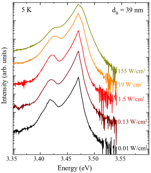
Figure 3(a) displays a streak camera image taken at 5 K on the sample with nm. Spectral profiles taken at various time delays are shown in Fig. 3(b). The PL decays exponentially with a decay time of 390 ps. This fast decay has a nonradiative origin and most probably arises from exciton recombination at point defects.Hauswald et al. (2014) Figure 3(c) shows PL intensity transients of the line at 5 and 50 K for the as-grown nanowires and for the quantum wire ensemble with nm. The integrated intensity of the line has been obtained by a spectral deconvolution of the transient spectra.Hauswald et al. (2013) Note that due to the significant spectral overlap between the and the transitions at the early stage of the decay [Fig. 3(b)], the values obtained for the PL intensities of the partially decomposed nanowire sample exhibit a comparatively large uncertainty for the initial 1 ns. At 5 K, the state for the as-grown nanowires decays exponentially, and the decay time ns is identical with the radiative lifetime . The PL decay for the quantum wires with nm is more complex: it is nonexponential during the first two ns after excitation, and becomes exponential with a decay time ns thereafter. Comparable results have been obtained for the sample with nm (not shown). Two different phenomena may, in principle, account for this initial nonexponential decay.
First, the discontinuity of the polarization field at the interfaces of I1 BSFs induces strong electrostatic fields along the nanowire axis, spatially separating the electron and hole wavefunctions.Sun et al. (2002); Lähnemann et al. (2012); Corfdir and Lefebvre (2012) A high initial carrier density created by pulsed excitation may screen these fields, giving rise to a minimum value for the radiative lifetime directly after excitation. Since the carrier density is subsequently reduced by recombination, the electric fields are restored again with time, resulting potentially in a continuous decrease in the energy as well as in a continuous increase in .Reale et al. (2003); Bretagnon et al. (2006) Since the recombination is purely radiative at low temperature [Fig. 2(a)], the latter increase could explain the nonexponential decay of the emission after pulsed excitation. However, the energy remains constant during the whole decay [Fig. 3(b)]. This finding suggests that the change in carrier density with time after pulsed excitation does not lead to strong modifications in the strength of built-in electric fields, and that the nonexponential PL decay seen in Fig. 3(c) is not due to the dynamical descreening of these fields. To confirm this result, we have recorded excitation-density dependent cw PL spectra at 5 K on the sample with nm (Fig. 4). Increasing the excitation density from 0.01 to 1.5 W/cm2 does not lead to any change in the energy of the , confirming that screening is negligible in this range of excitation densities.Reale et al. (2003) Note that the small blueshift observed for larger excitation densities most probably arises from band filling and/or heating effects (see the change in the and free exciton lineshapes when the density increases from 1.5 to 155 W/cm2). In view of the results in Figs. 3(b) and 4, it is unlikely that the nonexponential decay observed for the in the quantum wires [Fig. 3(c)] originates from the dynamical descreening of the built-in electric fields.
Second, the origin for the nonexponential decay may be associated with the pronounced tapering of the quantum wires. Since the BSFs are likely to occur at different positions along the nanowire axis, their radial dimension and thus the degree of radial confinement also varies. Since the radiative lifetime almost certainly depends on this degree of radial confinement,Kavokin (1994); Bellessa et al. (1998) a multiexponential decay would be an inevitable consequence. Following this interpretation, the experimental result of longer decay times for the quantum wires implies that the radiative lifetime increases with decreasing diameter. We will return to this issue after a discussion of the transients at 50 K and the temperature dependence of .
At a temperature of 50 K, for which the PL intensity of our samples is still close to that at 5 K [cf. Fig. 2(a)], the decay of the remains exponential for the as-grown nanowires, but increases from 1.0 to 4.2 ns. In contrast, the increased temperature does not affect the decay of the for the quantum wires. Figure 3(d) shows the evolution of between 5 and 120 K for both samples. Up to a temperature of 50–60 K, the decay of the is purely radiative and . Between 15 and 40 K, increases nearly linearly for the as-grown nanowires, demonstrating that (i) I1 BSFs in nanowires with a diameter of 51 nm act as quantum wells,Corfdir et al. (2011) and (ii) the is free to move along the BSF plane. The deviation from a linear behavior for temperatures lower than 15 K arises from exciton localization along the BSF plane due to the presence of donors as discussed in Ref. Corfdir et al., 2014. The significant reduction in for temperatures larger than 60 K is due to the thermal escape of excitons from the BSF plane. For the quantum wires, the long component of the nonexponential decay is independent of temperature and corresponds to the radiative lifetime of the in the thinnest nanowire segments according to the discussion above. The constant lifetime confirms unambiguously that BSFs in GaN quantum wires behave as crystal-phase quantum dots. The reduction of the dimensionality of the state from two to zero already when nm again suggests that the crystal-phase quantum dots are located in the top part of the nanowires, where the diameter is much smaller.
Finally, we address the origin of the increase in with decreasing diameter observed above. Considering that the exciton is coherent over the entire BSF, the radiative decay rate can be written approximately as:Brandt et al. (1992); Kavokin (1994)
| (1) |
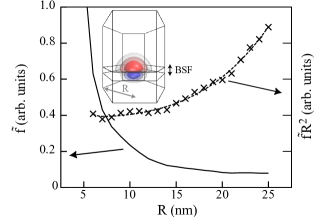
with the oscillator strength per unit area , the coherence area (which is assumed to be determined by the nanowire’s radius ),Brandt et al. (1992); Kavokin (1994); Bellessa et al. (1998) the overlap integral between the electron and hole wavefunctions along the nanowire axis , and the Bohr radius of the exciton in the BSF plane . For examining the change of with a decrease in , we calculate the wavefunction of the in nanowires of diameters between 10 and 50 nm using eight-band calculations.Marquardt et al. (2014) The BSF within the GaN nanowire is represented by 3 monolayers of zincblende GaN within a wurtzite GaN segment of 20 nm length. The nanowires are considered to be undoped, i. e., surface potentials are absent. The surface is considered as an infinite potential barrier. The spontaneous polarization of wurtzite GaN induces axial electrostatic fields in the BSF with a magnitude of 3 MV/cm.Corfdir and Lefebvre (2012) We average over all polarization directions, i. e., the oscillator strength is simply given by .
Figure 5 shows the dependence of and as a function of . As shown in the inset of Fig. 5 for a diameter of 20 nm, both the electron and the hole are located in the center of the quantum disk. With decreasing , the electron experiences a progressively stronger confinement which results in a strong increase of as displayed in Fig. 5. A radial separation between the electron and hole wavefunctions as observed in Ref. Marquardt et al., 2014 does not occur for the range of nanowire diameters considered here, a finding that still holds when considering the presence of surface potentials due to Fermi level pinning at the free sidewalls and a homogeneous background doping of cm-3 (not shown here). The increase in with decreasing should result in a decrease in , in contradiction to our experimental observation [cf. Fig. 3(c,d)].
As shown in Fig. 5, the dependence of the radiative decay rate on diameter is reversed when taking into account the factor in Eq. (1). This factor accounts for the fact that the exciton’s radiative decay is enhanced by its coherent macroscopic polarization.Brandt et al. (1992); Kavokin (1994); Bellessa et al. (1998) This enhanced radiative decay may also be understood in the context of the arguments of Rashba and Gurgenishvili (1962): the larger the coherence area of the exciton, the smaller the spread of its wavefunction in k space and thus the shorter . As shown in Fig. 5, the total oscillator strength is indeed predicted to decrease with decreasing , and the radiative lifetime is thus expected to increase correspondingly in agreement with the experiment.
To conclude, changing the diameter of GaN nanowires in a controlled fashion has allowed us to observe the transition from two- to zero-dimensional stacking-fault bound excitons. This transition occurs at diameters significantly larger than the exciton’s Bohr radius and is induced by dielectric confinement. Because of the absence of structural imperfections such as interfacial steps and alloy fluctuations, the radiative decay rate of these excitons scales with the nanowire diameter, which imposes a geometrical limitation of their coherence area.
We thank Alberto Hernández-Mínguez for carefully reading our manuscript. Partial funding from the Deutsche Forschungsgemeinschaft within SFB 951 is gratefully acknowledged. P.C. acknowledges partial funding from the Fonds National Suisse de la Recherche Scientifique through project 161032.
References
- Zettler et al. (2015) J. K. Zettler, C. Hauswald, P. Corfdir, M. Musolino, L. Geelhaar, H. Riechert, O. Brandt, and S. Fernández-Garrido, Cryst. Growth Des. 15, 4104 (2015).
- Hersee et al. (2011) S. D. Hersee, A. K. Rishinaramangalam, M. N. Fairchild, L. Zhang, and P. Varangis, J. Mat. Res. 26, 2293 (2011).
- Kishino and Ishizawa (2015) K. Kishino and S. Ishizawa, Nanotechnology 26, 225602 (2015).
- Bao et al. (2008) J. Bao, D. C. Bell, F. Capasso, J. B. Wagner, T. Mårtensson, J. Trägårdh, and L. Samuelson, Nano Lett. 8, 836 (2008).
- Corfdir et al. (2013) P. Corfdir, B. Van Hattem, E. Uccelli, S. Conesa-Boj, P. Lefebvre, A. Fontcuberta i Morral, and R. T. Phillips, Nano Lett. 13, 5303 (2013).
- Calleja et al. (2007) E. Calleja, J. Ristić, S. Fernández-Garrido, L. Cerutti, M. A. Sánchez-García, J. Grandal, A. Trampert, U. Jahn, G. Sánchez, A. Griol, and B. Sánchez, Phys. Status Solidi B 244, 2816 (2007).
- Geelhaar et al. (2011) L. Geelhaar, C. Chèze, B. Jenichen, O. Brandt, C. Pfüller, S. Münch, R. Rothemund, S. Reitzenstein, A. Forchel, T. Kehagias, P. Komninou, G. P. Dimitrakopulos, T. Karakostas, L. Lari, P. R. Chalker, M. H. Gass, and H. Riechert, IEEE J. Sel. Top. Quantum Electro. 17, 878 (2011).
- Corfdir et al. (2014) P. Corfdir, C. Hauswald, J. K. Zettler, T. Flissikowski, J. Lähnemann, S. Fernández-Garrido, L. Geelhaar, H. T. Grahn, and O. Brandt, Phys. Rev. B 90, 195309 (2014).
- Korona et al. (2014) K. P. Korona, A. Reszka, M. Sobanska, P. Perkowska, A. Wysmołek, K. Klosek, and Z. R. Zytkiewicz, J. Lumin. 155, 293 (2014).
- Stampfl and Van de Walle (1998) C. Stampfl and C. G. Van de Walle, Phys. Rev. B 57, R15052 (1998).
- Akopian et al. (2010) N. Akopian, G. Patriarche, L. Liu, J.-C. Harmand, and V. Zwiller, Nano Lett. 10, 1198 (2010).
- Zettler et al. (2016) J. K. Zettler, P. Corfdir, C. Hauswald, E. Luna, U. Jahn, T. Flissikowski, E. Schmidt, C. Ronning, A. Trampert, L. Geelhaar, H. T. Grahn, O. Brandt, and S. Fernández-Garrido, Nano Lett. 16, 973 (2016).
- Loitsch et al. (2015) B. Loitsch, D. Rudolph, S. Morkötter, M. Döblinger, G. Grimaldi, L. Hanschke, S. Matich, E. Parzinger, U. Wurstbauer, G. Abstreiter, J. J. Finley, and G. Koblmüller, Adv. Mater. , 2195 (2015).
- Keldysh (1979) L. V. Keldysh, Pis´ma Zh. Eksp. Teor. Fiz. 29, 716 (1979), [JETP Lett. 29, 658 (1979)].
- Kumagai and Takagahara (1989) M. Kumagai and T. Takagahara, Phys. Rev. B 40, 12359 (1989).
- Consonni et al. (2009) V. Consonni, M. Knelangen, U. Jahn, A. Trampert, L. Geelhaar, and H. Riechert, Appl. Phys. Lett. 95, 241910 (2009).
- Graham et al. (2013) A. M. Graham, P. Corfdir, M. Heiss, S. Conesa-Boj, E. Uccelli, A. Fontcuberta i Morral, and R. T. Phillips, Phys. Rev. B 87, 125304 (2013).
- Rudolph et al. (2013) D. Rudolph, L. Schweickert, S. Morkötter, L. Hanschke, S. Hertenberger, M. Bichler, G. Koblmüller, G. Abstreiter, and J. J. Finley, New J. Phys. 15, 113032 (2013).
- Hauswald et al. (2014) C. Hauswald, P. Corfdir, J. K. Zettler, V. M. Kaganer, K. K. Sabelfeld, S. Fernández-Garrido, T. Flissikowski, V. Consonni, T. Gotschke, H. T. Grahn, L. Geelhaar, and O. Brandt, Phys. Rev. B 90, 165304 (2014).
- Hauswald et al. (2013) C. Hauswald, T. Flissikowski, T. Gotschke, R. Calarco, L. Geelhaar, H. T. Grahn, and O. Brandt, Phys. Rev. B 88, 075312 (2013).
- Sun et al. (2002) Y. J. Sun, O. Brandt, U. Jahn, T. Y. Liu, A. Trampert, S. Cronenberg, S. Dhar, and K. H. Ploog, J. Appl. Phys. 92, 5714 (2002).
- Lähnemann et al. (2012) J. Lähnemann, O. Brandt, U. Jahn, C. Pfüller, C. Roder, P. Dogan, F. Grosse, A. Belabbes, F. Bechstedt, A. Trampert, and L. Geelhaar, Phys. Rev. B 86, 081302 (2012).
- Corfdir and Lefebvre (2012) P. Corfdir and P. Lefebvre, J. Appl. Phys. 112, 053512 (2012).
- Reale et al. (2003) A. Reale, G. Massari, A. Di Carlo, P. Lugli, A. Vinattieri, D. Alderighi, M. Colocci, F. Semond, N. Grandjean, and J. Massies, J. Appl. Phys. 93, 400 (2003).
- Bretagnon et al. (2006) T. Bretagnon, P. Lefebvre, P. Valvin, R. Bardoux, T. Guillet, T. Taliercio, B. Gil, N. Grandjean, F. Semond, B. Damilano, A. Dussaigne, and J. Massies, Phys. Rev. B 73, 113304 (2006).
- Kavokin (1994) A. V. Kavokin, Phys. Rev. B 50, 8000 (1994).
- Bellessa et al. (1998) J. Bellessa, V. Voliotis, R. Grousson, X. L. Wang, M. Ogura, and H. Matsuhata, Phys. Rev. B 58, 9933 (1998).
- Corfdir et al. (2011) P. Corfdir, J. Levrat, A. Dussaigne, P. Lefebvre, H. Teisseyre, I. Grzegory, T. Suski, J.-D. Ganière, N. Grandjean, and B. Deveaud-Plédran, Phys. Rev. B 83, 245326 (2011).
- Humphrey et al. (1996) W. Humphrey, A. Dalke, and K. Schulten, J. Mol. Graph. 14, 33 (1996).
- Brandt et al. (1992) O. Brandt, G. C. La Rocca, A. Heberle, A. Ruiz, and K. Ploog, Phys. Rev. B 45, 3803 (1992).
- Marquardt et al. (2014) O. Marquardt, S. Boeck, C. Freysoldt, T. Hickel, S. Schulz, J. Neugebauer, and E. P. O’Reilly, Comp. Mat. Sci. 95, 280 (2014).
- Rashba and Gurgenishvili (1962) E. I. Rashba and G. E. Gurgenishvili, Fiz. Tverd. Tela 4, 1029 (1962), [Sov. Phys. - Solid State 4, 759 (1962)].