Efficient polarization insensitive complex wavefront control using Huygens’ metasurfaces based on dielectric resonant meta-atoms
Abstract
Subwavelength-thin metasurfaces have shown great promises for the control of optical wavefronts, thus opening new pathways for the development of efficient flat optics. In particular, Huygens’ metasurfaces based on all-dielectric resonant meta-atoms have already shown a huge potential for practical applications with their polarization insensitivity and high transmittance efficiency. Here, we experimentally demonstrate a polarization insensitive holographic Huygens’ metasurface based on dielectric resonant meta-atoms capable of complex wavefront control at telecom wavelengths. Our metasurface produces a hologram image in the far-field with 82% transmittance efficiency and 40% imaging efficiency. Such efficient complex wavefront control shows that Huygens’ metasurfaces based on resonant dielectric meta-atoms are a big step towards practical applications of metasurfaces in wavefront design related technologies, including computer-generated holograms, ultra-thin optics, security and data storage devices.
keywords:
Wavefront control, Huygens’ surface, Metasurface, HolographyInstitute of Applied Physics, Abbe Center of Photonics, Friedrich-Schiller-University Jena, 07743 Jena, Germany \abbreviationsIR,NMR,UV
The ability to perform wavefront control using optical metasurfaces has gained significant attention in recent years as it provides a route to ultra-thin optics that can potentially replace all bulky optical components 1, 2, 3. A number of studies have demonstrated the wavefront control capabilities of optical metasurfaces by realizing various flat optical elements, including beam deflectors 4, 5, 6, beam shapers 4, 7, 8, 5, 9, flat lenses 10, 7, 11, and holograms 12, 13. Metasurface holograms, in particular, represent the ultimate examples of complex wavefront control, as they can transform an incident plane wave into a desired arbitrary wavefront in the far-field. As such, a number of groups have developed optical holographic metasurfaces 12, 13, 14, 15, 16, 17, 18, 19, 11, 20 aiming at applications such as holographic displays, data storage and optical tweezers. While borrowing from the vast knowledge of the field of computer generated holograms, metasurface holograms enable, for the first time, ultra-high efficiency of the image reconstruction based on a single-step lithographic process. Indeed, efficiencies of holographic reproduction in metasurfaces of more than 80% have been demonstrated recently 19, 21.
However, most metasurfaces to date are based on plasmonic elements that are intrinsically lossy in the optical spectral region due to the absorption in metals 1, 2, 3. In addition, the need for the ability to control the optical phase-front in the full range of imposes more restrictions on the design parameters of metasurfaces, therefore leading to the introduction of several undesirable losses, including reflection, diffraction and polarization conversion losses. These issues have triggered a rapid move towards all-dielectric metasurfaces 5, 9, 11, 22, 23. While dielectric resonators in the microwave regime are known since the 80s 24 and earlier, dielectric metasurfaces in the optical regime have attracted great interest only recently. By exploring resonant effects in dielectric nanostructures 23, 5, 6, 25, 9, 11, 26, 27, 8, 28, 29, 30, 31, 32, 33, 22 that exhibit significantly lower losses than their metallic counterparts, such all-dielectric metasurfaces can offer practical solutions for a diverse range of efficient wave-shaping applications 22, 9, 8, 11.
Out of this large body of work, the concept of Huygens’ 34 dielectric metasurfaces 22 has proven to be an important advance for achieving full phase control and high transmittance efficiencies. Huygens’ metasurfaces rely on the overlap of the electric and magnetic resonances of the high-index dielectric nanoparticles 35 to provide full phase coverage and complete elimination of reflection losses. These particles furthermore show polarization insensitive operation 9, 6 while, at the same time, absorption losses are negligible due to the use of lossless high-index dielectric materials.
Following this progress, recent works have demonstrated that all-dielectric Huygens’ metasurfaces consisting of silicon nanoparticle arrays 22 enable efficient wavefront control, where the spatial variation of the phase can be achieved by tuning the lattice periodicity 9 or nanoparticle dimensions 23, 22, 6, 33. Such convenient control of the spatially dependent transmittance phase of the arrays, as required for wavefront shaping, has enabled the demonstration of some basic functionalities, including Gaussian-to-vortex beam shaping 9, 33 and beam deflecting 6, 33. However, simple wavefront control with a homogeneous phase profile (in either linear or azimuthal directions) across a metasurface can provide only limited functionalities.
One of the main capabilities of metasurfaces is the on-demand generation of arbitrary wavefronts. An on-demand metasurface is able to imprint arbitrarily complex wavefronts on incident light with an inhomogeneous phase profile and thereby realize holographic images of any designs. Despite the desirability of such a metasurface, the well-sought capability of complex wavefront control has not yet been demonstrated with both high efficiency and polarization independence.
Here, we experimentally realize a dielectric holographic metasurface that produces an arbitrarily designed hologram image to demonstrate complex wavefront control. Our holographic metasurface has a 82% transmittance efficiency and a 40% imaging efficiency, where the latter value represents the total amount of light that ends up in the pre-defined hologram pattern (see Method section). These high efficiency values make our metasurface the most efficient polarization insensitive holographic metasurfaces to-date.
Additionally, while existing computer-generated-holographic technology can also produce arbitrarily designed hologram images, most of these holograms rely on diffractive optics that require multi-step lithography processes, which by itself could lead to alignment and other fabrication errors36, 37. Furthermore, conventional holography suffers from other disadvantages, including the twin image generation that fundamentally limits the hologram efficiency as well as the strong polarization sensitivity due to the holographic gratings. Here, our holographic metasurface presents a completely new approach to holography by using lossless resonant meta-atoms as Huygens’ sources, fabricated in a single step in the lithography process. This opens the door to incorporating all types of metasurface functionalities as well as resolving problems with existing computer-generated-holograms.
Figure 1(a) shows a conceptual image of our experiment; a monochromatic laser beam ( nm) passes through a holographic Huygens’ metasurface which acts as a phase mask to modulate the wavefront of the incident beam, thereby generating a holographic image of the letters “h” 12 mm behind the sample.
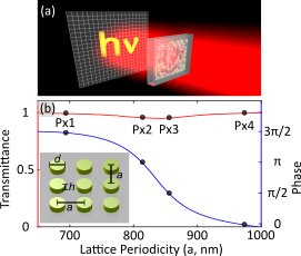
In order to experimentally realize the holographic metasurface, we employ silicon nanodisks as meta-atoms, which have previously allowed the realization of polarization insensitive beam-shaping metasurfaces with high transmittance efficiencies 22, 9. All nanodisks forming the metasurface have the same diameter and the same height, and are embedded into a nm thick layer of silicon dioxide (silica). The height of the silicon nanodisks is set to nm. The diameter of nm has been chosen to tune the electric and magnetic dipole resonances into spectral overlap, which enables a phase shift at the resonance 22, thereby providing a full range of accessible phase values.
The spatial gradient of transmittance phases in the metasurface plane required for holographic image generation is obtained by the local variation of the lattice periodicity only. Since a variation of lattice periodicity would lead to a spectral shift of the resonance, the spatial transmittance phases introduced at a particular frequency would then be dependent on the range of lattice periodicity selected. Our operation wavelength of 1477 nm is chosen such that the silicon nanodisk arrays with the selected parameters provide the largest range of transmittance phases for a physically realizable variation of lattice periodicity, as well as the highest transmittance across the same range of lattice periodicity values. Fig. 1(b) shows the numerically calculated transmittance intensities and phases of the four optimized silicon nanodisk arrays. A schematic of an example array is shown in the inset of Fig. 1(b).
The range of transmittance phases accessible by the variation of the lattice periodicity for our metasurface is , as shown in Fig. 1(b), and is only limited due to our choice of using only one tuning parameter (the lattice periodicity ). Although the maximum phase range can easily be extended by additionally changing the diameter and/or the height of the nanodisks, our design can already allow for a simple, discretized and pixelated implementations of the metasurface with equidistant phase steps, namely a four-level phase mask with phase steps of . The selected phase values are denoted by black dots on the blue curve in Fig. 1(b), showing the corresponding lattice periodicities of nm, nm, nm, and nm. The close-to-unity transmittance of the nanodisk arrays with the selected periodicities is also shown as black dots on red curve in Fig. 1(b).
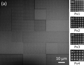
For fabrication of the silicon nanodisk metasurface, we use electron-beam lithography (EBL) on a back side polished silicon-on-insulator (SOI) wafer, followed by reactive-ion etching of the top silicon layer. The resulting nanodisks are then embedded in a 580 nm thick silica layer by low-pressure chemical vapor deposition (LPCVD). More details of the fabrication process can be found in the Method section. Fig. 2(a) shows the scanning-electron microscopy (SEM) image of a small section of a typical fabricated sample before LPCVD. Figs. 2(b)-(e) show magnified views of the structure from each of the four realized pixel types characterized by their lattice periodicities.
For the arrangement of the pixels in the metasurfaces, we calculate the phase mask required for a particular input image using the Gerchberg-Saxton algorithm 38 and the angular spectrum method 39. The calculation uses the source image shown in Fig. 3(a), and several selected parameters, namely the resolution of the hologram image (28x28 pixels), pixel size (17.35x17.35 m) and the distance of the hologram image from the phase mask (12 mm), to compute the phase mask pattern required to reproduce the source image as a hologram. These parameters are chosen in order to provide a high-quality hologram while at the same time keeping the EBL exposure time reasonably short. Naturally, larger writing fields (more pixels) allow for higher-resolution and more complex holograms. On the other hand, increasing the number of pixels under a restricted EBL writefield size of 500x500m can also enhance the hologram resolution. However, minimizing the pixel size will affect the performance of the metasurface due to interparticle coupling effects or disturbances at the pixel borders, which are not taken into account in our design. Hence, the current pixel size of 17.35x17.35 m was carefully chosen to balance all of these factors.
Figure 3(b) shows the calculated phase mask where the four distinct colors represent the phase shifts imprinted onto the incident wave in different spatial positions to generate the hologram image. A simulated image (Fig. 3(c)) of the reproduced hologram is also calculated by numerically propagating a 1477 nm plane wave through the phase mask pattern generated previously. A true-color optical microscopy image at visible wavelengths of the fabricated phase mask, where the required phase shifts have been translated into silicon nanodisk arrays of the respective lattice periodicities, is shown in Fig. 3(d), and can be compared directly with the original design in Fig. 3(b).
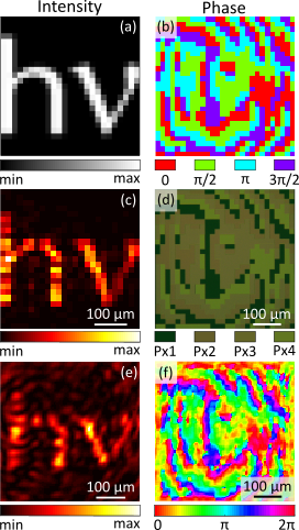
To optically characterize our holographic metasurface phase mask, we first observe the generated hologram by transmitting a linearly polarized 1477 nm laser beam through the sample and imaging the hologram plane 12 mm behind the sample onto an Infrared (IR) camera. The obtained image is shown in Fig. 3(e), clearly showing the letters “h, where the bright and dark features, as well as the size of the letters, agree very well with the calculated hologram in Fig. 3(c). Next, we measure the phase of the generated hologram by recording a set of four interferograms using a home-built Mach-Zehnder interferometer with the same laser source and IR camera as used for imaging. Based on these measurements, we perform a phase retrieval process 40. The reconstructed experimental phase shown in Fig. 3(f) is in good agreement with the calculated phase in Fig. 3(b).
While our holographic metasurface has been optimized for the operational wavelength of 1477 nm, this device can also operate and create visually similar hologram images within nm of 1477 nm. This bandwidth of 40 nm is dependent on and limited by the resonance width of the dipole resonances. Such dispersive behavior associated with the narrow resonances provides additional degrees of freedom for engineering optical responses. While a weakly dispersive metasurface will show a similar optical response for a broad range of frequencies, a resonant metasurfaces can in principle allow for tailoring a frequency selective response, e.g. displaying different holographic images for different colors.
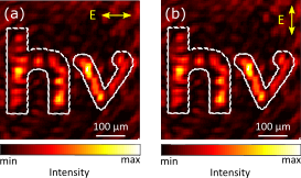
In order to provide a quantitative evaluation of the performance of the realized holographic metasurface, we measured the transmittance efficiency using an IR camera. The transmittance efficiency of the holographic metasurface is measured to be 82% for horizontal and vertical polarizations. Additionally, we measure the imaging efficiencies of the metasurfaces, i.e. the total amount of light that ends up in the letters “h, by masking the recorded hologram image as indicated by the dashed lines in Fig. 4. The imaging efficiency is measured as 39% and 40% for horizontal and vertical polarizations respectively. Details of the measurement method and definitions of the efficiencies are explained in the Method section.
Our imaging efficiency can be further improved by increasing the numbers of pixel of our hologram and reducing the pixel size. In this proof-of-principle experiment, the imaging efficiency and resolution of the hologram are limited by the writing time in the EBL process and our choice of source image resolution in order to produce a phase profile with more connecting pixels for each phase level to minimize stitching errors and proximity effects. Further optimization of the hologram quality can be achieved for smaller pixel sizes, however large scale numerical simulations are needed to take into account the meta-atom interactions at pixel borders. Therefore, higher quality hologram images can in principle be achieved.
The visually identical hologram images recorded for the two polarizations, as shown in Figs. 4(a) and (b) furthermore directly confirm the polarization insensitivity of the metasurface hologram, a property which cannot be achieved using holographic metasurfaces based on the acquisition of geometric phase.
In conclusion, we have demonstrated complex wavefront control using a highly efficient polarization-insensitive holographic Huygens’ metasurface based on resonant silicon meta-atoms. By varying only one geometrical parameter (lattice periodicity) that can be controlled easily during the fabrication process, we can effectively generate arbitrary hologram images with four phase-discretization levels. The transmission efficiency and the imaging efficiency of our device is measured to be as high as 82% and 40% respectively. The functionality of our holographic Huygens’ metasurface is polarization insensitive and therefore allowing it to be used in any optical system without pre-conditioning the incident beam, unlike metasurfaces that exploit geometric phase. Notably, by simply choosing an asymmetric design of the meta-atoms, one can also realize polarization sensitive holographic Huygens’ metasurfaces, if required. By further increasing the number of phase levels of the hologram and reducing the size of the pixels, the hologram efficiency, resolution, and complexity can be further increased, leading to potential applications in holographic displays, data storage and security devices based on computer-generated holography.
1 Method
1.1 Fabrication
For fabrication of the holographic metasurface, we performed electron-beam lithography (EBL) on a backside polished silicon-on-insulator wafer (243 nm top silicon thickness, 3 m buried oxide thickness). We first cleaned the top silicon surface by oxygen plasma (2 min, 200 W), then spin-coated HMDS as an adhesion promoter (3000 rpm, 30 s) and followed by spin-coating of the negative-tone electron-beam resist NEB-31A(3000 rpm, 30 s). The resulting resist thickness is about 300 nm. We performed both a pre-exposure bake (100 ∘C, 2 min) and a post-exposure bake (90 ∘C, 1 min). After electron-beam exposure (400 pA beam), development was performed using the MF-321 developer with a development time of 75 s, followed by a rinse in de-ionized water for several minutes. The resulting resist pattern was then used as an etch mask for an inductively coupled plasma (ICP) etching process (25 W RF power, 300 W ICP power, 60 ∘C) using Ar (40 sccm) and HBr (15 sccm) as etch gases. Ar/Cl2 plasma chemistry is used for native oxide breakthrough. Remaining resist was removed using oxygen plasma and piranha solution. Finally, the sample is coated with a 580 nm thick silica layer by low pressure vapor deposition (LPCVD).
1.2 Efficiency Measurement
In order to provide a quantitative evaluation of the performance of the realized holographic metasurface, we derive the transmittance efficiency of the metasurface as the total intensity of the light going through the metasurface referenced to the intensity passing through an etched but unstructured area of the sample of equal size. This way, we eliminate the reflections from the handle wafer, which are not relevant for the performance of the actual metasurface.
In addition to the transmittance intensity, we furthermore calculate the imaging efficiency, i.e., the total amount of light forming the pre-defined hologram pattern, the letters “h, as recorded on the IR camera, divided by the amount of light passing through the same referenced area as in the transmittance efficiency case. To calculate the intensity of the light that forms the letters “h, we mask the recorded hologram image as indicated by the dashed lines in Fig. 4.
As the intensity distributions of the hologram in the image plane has a dynamic range exceeding that of the camera used in our experiments, multiple images were taken at different intensity levels of the incident laser beam using neutral density filters. This way it is possible to reconstruct the full dynamic range of the images to retrieve accurate intensity values and hence more accurate efficiency values.
This work was performed, in part, at the Center for Integrated Nanotechnologies, an Office of Science User Facility operated for the U.S. Department of Energy (DOE) Office of Science. Sandia National Laboratories is a multi-program laboratory managed and operated by Sandia Corporation, a wholly owned subsidiary of Lockheed Martin Corporation, for the U.S. Department of Energy’s National Nuclear Security Administration under contract DE-AC04-94AL85000.
K.E.C. acknowledges the support from the Australian Nanotechnology Network Overseas Travel Fellowships 2014 and the Australian National University Vice Chancellor’s HDR Travel Grants 2014. K.E.C., I.S., M.D., D.N. and Y.S.K. also acknowledge their participation in the Erasmus Mundus NANOPHI project, contract number 2013 5659/002-001. The authors also acknowledge a support from the Australian Research Council.
References
- Yu and Capasso 2014 Yu, N.; Capasso, F. Flat optics with designer metasurfaces. Nat. Mater. 2014, 13, 139–150
- Minovich et al. 2015 Minovich, A. E.; Miroshnichenko, A. E.; Bykov, A. Y.; Murzina, T. V.; Neshev, D. N.; Kivshar, Y. S. Functional and nonlinear optical metasurfaces. Laser Photon Rev. 2015, 9, 195–213
- Genevet and Capasso 2015 Genevet, P.; Capasso, F. Holographic optical metasurfaces: a review of current progress. Rep. Prog. Phys. 2015, 78, 024401
- Yu et al. 2011 Yu, N.; Genevet, P.; Kats, M. A.; Aieta, F.; Tetienne, J.-P.; Capasso, F.; Gaburro, Z. Light propagation with phase discontinuities: generalized laws of reflection and refraction. Science 2011, 334, 333–337
- Lin et al. 2014 Lin, D.; Fan, P.; Hasman, E.; Brongersma, M. L. Dielectric gradient metasurface optical elements. Science 2014, 345, 298–302
- Yu et al. 2015 Yu, Y. F.; Zhu, A. Y.; Paniagua-Domínguez, R.; Fu, Y. H.; Luk’yanchuk, B.; Kuznetsov, A. I. High-transmission dielectric metasurface with 2 phase control at visible wavelengths. Laser Photon Rev. 2015, 9, 412–418
- Aieta et al. 2012 Aieta, F.; Genevet, P.; Kats, M. A.; Yu, N.; Blanchard, R.; Gaburro, Z.; Capasso, F. Aberration-free ultrathin flat lenses and axicons at telecom wavelengths based on plasmonic metasurfaces. Nano Lett. 2012, 12, 4932–4936
- Yang et al. 2014 Yang, Y.; Wang, W.; Moitra, P.; Kravchenko, I. I.; Briggs, D. P.; Valentine, J. Dielectric meta-reflectarray for broadband linear polarization conversion and optical vortex generation. Nano Lett. 2014, 14, 1394–1399
- Chong et al. 2015 Chong, K. E.; Staude, I.; James, A.; Dominguez, J.; Liu, S.; Campione, S.; Subramania, G. S.; Luk, T. S.; Decker, M.; Neshev, D. N.; Brener, I.; Kivshar, Y. S. Polarization-independent silicon metadevices for efficient optical wavefront control. Nano Lett. 2015, 15, 5369–5374
- Hasman et al. 2003 Hasman, E.; Kleiner, V.; Biener, G.; Niv, A. Polarization dependent focusing lens by use of quantized Pancharatnam-Berry phase diffractive optics. Appl. Phys. Lett 2003, 82, 328–330
- Arbabi et al. 2015 Arbabi, A.; Horie, Y.; Ball, A. J.; Bagheri, M.; Faraon, A. Subwavelength-thick lenses with high numerical apertures and large efficiency based on high contrast transmitarrays. Nat. Commun. 2015, 6, 1–10
- Ni et al. 2013 Ni, X.; Kildishev, A. V.; Shalaev, V. M. Metasurface holograms for visible light. Nat. Commun. 2013, 4, 2807
- Huang et al. 2013 Huang, L.; Chen, X.; Mühlenbernd, H.; Zhang, H.; Chen, S.; Bai, B.; Tan, Q.; Jin, G.; Cheah, K.-W.; Qiu, C.-W.; Li, J.; Zentgraf, T.; Zhang, S. Three-dimensional optical holography using a plasmonic metasurface. Nat. Commun. 2013, 4, 2808
- Zhou et al. 2013 Zhou, F.; Liu, Y.; Cai, W. Plasmonic holographic imaging with V-shaped nanoantenna array. Opt. Express 2013, 21, 4348
- Lin et al. 2013 Lin, J.; Genevet, P.; Kats, M. A.; Antoniou, N.; Capasso, F. Nanostructured holograms for broadband manipulation of vector beams. Nano Lett. 2013, 13, 4269–4274
- Chen et al. 2014 Chen, W. T.; Yang, K.-Y.; Wang, C.-M.; Huang, Y.-W.; Sun, G.; Liao, C. Y.; Hsu, W.-L.; Lin, H. T.; Sun, S.; Zhou, L.; Liu, A. Q.; Tsai, D. P. High-efficiency broadband meta-hologram with polarization-controlled dual images. Nano Lett. 2014, 14, 225–230
- Montelongo et al. 2014 Montelongo, Y.; Tenorio-Pearl, J. O.; Williams, C.; Zhang, S.; Milne, W. I.; Wilkinson, T. D. Plasmonic nanoparticle scattering for color holograms. Proc. Natl. Acad. Sci. U. S. A. 2014, 111, 1–5
- Zheng et al. 2014 Zheng, J.; Ye, Z.-C.; Sun, N.-L.; Zhang, R.; Sheng, Z.-M.; Shieh, H.-P. D.; Zhang, J. Highly anisotropic metasurface: a polarized beam splitter and hologram. Sci. Rep. 2014, 4, 6491
- Zheng et al. 2015 Zheng, G.; Mühlenbernd, H.; Kenney, M.; Li, G.; Zentgraf, T.; Zhang, S. Metasurface holograms reaching 80% efficiency. Nat. Nanotech. 2015, 10, 308–12
- Lalanne et al. 1998 Lalanne, P.; Astilean, S.; Chavel, P.; Cambril, E.; Launois, H. Blazed binary subwavelength gratings with efficiencies larger than those of conventional échelette gratings. Opt. Lett. 1998, 23, 1081–1083
- 21 Arbabi, A.; Horie, Y.; Bagheri, M.; Faraon, A. Dielectric metasurfaces for complete control of phase and polarization with subwavelength spatial resolution and high transmission. Nat. Nanotech. advance online publication, 31 August 2015 (DOI 10.1038/nnano.2015.186)
- Decker et al. 2015 Decker, M.; Staude, I.; Falkner, M.; Dominguez, J.; Neshev, D. N.; Brener, I.; Pertsch, T.; Kivshar, Y. S. High-efficiency dielectric Huygens’ surfaces. Adv. Opt. Mater. 2015, 3, 813–820
- Staude et al. 2013 Staude, I.; Miroshnichenko, A. E.; Decker, M.; Fofang, N. T.; Liu, S.; Gonzales, E.; Dominguez, J.; Luk, T. S.; Neshev, D. N.; Brener, I.; Kivshar, Y. Tailoring directional scattering through magnetic and electric resonances in subwavelength silicon nanodisks. ACS Nano 2013, 7, 7824–7832
- Kajfez and Guillon 1986 Kajfez, D.; Guillon, P. Dielectric Resonators; Artech House, Inc.: Dedham, MA, 1986
- Yang et al. 2014 Yang, Y.; Kravchenko, I. I.; Briggs, D. P.; Valentine, J. All-dielectric metasurface analogue of electromagnetically induced transparency. Nat. Commun. 2014, 5, 5753
- Bomzon et al. 2002 Bomzon, Z.; Biener, G.; Kleiner, V.; Hasman, E. Space-variant Pancharatnam-Berry phase optical elements with computer-generated subwavelength gratings. Opt. Lett. 2002, 27, 1141–1143
- Levy et al. 2005 Levy, U.; Kim, H.-C.; Tsai, C.-H.; Fainman, Y. Near-infrared demonstration of computer-generated holograms implemented by using subwavelength gratings with space-variant orientation. Opt. Lett. 2005, 30, 2089–2091
- Wu et al. 2014 Wu, C.; Arju, N.; Kelp, G.; Fan, J. A.; Dominguez, J.; Gonzales, E.; Tutuc, E.; Brener, I.; Shvets, G. Spectrally selective chiral silicon metasurfaces based on infrared Fano resonances. Nat. Commun. 2014, 5, 3892
- Chong et al. 2014 Chong, K. E.; Hopkins, B.; Staude, I.; Miroshnichenko, A. E.; Dominguez, J.; Decker, M.; Neshev, D. N.; Brener, I.; Kivshar, Y. S. Observation of Fano resonances in all-dielectric nanoparticle oligomers. Small 2014, 10, 1985–1990
- Horasaninejad and Hu 2015 Horasaninejad, M. K.; Hu, W. Z. Efficient polarization beam splitter pixels based on a dielectric metasurface. Optica 2015, 2, 376–382
- Iyer et al. 2015 Iyer, P. P.; Butakov, N. a.; Schuller, J. a. Reconfigurable semiconductor phased-array metasurfaces. ACS Photon. 2015, 2, 1077–1084
- 32 Desiatov, B.; Mazurski, N.; Fainman, Y.; Levy, U. Polarization selective beam shaping using nanoscale dielectric metasurfaces. Opt. Express 22611
- Shalaev et al. 2015 Shalaev, M. I.; Sun, J.; Tsukernik, A.; Pandey, A.; Nikolskiy, K.; Litchinitser, N. M. High-efficiency all-dielectric metasurfaces for ultracompact beam manipulation in transmission mode. Nano Lett. 2015, 15, 6261–6266
- Pfeiffer and Grbic 2013 Pfeiffer, C.; Grbic, A. Metamaterial Huygens’ surfaces: tailoring wave fronts with reflectionless sheets. Phy. Rev. Lett. 2013, 110, 197401
- Evlyukhin et al. 2011 Evlyukhin, A. B.; Reinhardt, C.; Chichkov, B. N. Multipole light scattering by nonspherical nanoparticles in the discrete dipole approximation. Phys. Rev. B 2011, 84, 235429
- Freese et al. 2010 Freese, W.; Kämpfe, T.; Kley, E.-B.; Tünnermann, A. Design of binary subwavelength multiphase level computer generated holograms. Opt. Lett. 2010, 35, 5
- Scheuer and Yifat 2015 Scheuer, J.; Yifat, Y. Holography: Metasurfaces make it practical. Nat. Nanotech. 2015, 10, 296–298
- Gerchberg and Saxton 1972 Gerchberg, R. W.; Saxton, W. O. A practical algorithm for the determination of the phase from image and diffraction plane pictures. Optik 1972, 35, 237–246
- Matsushima and Shimobaba 2009 Matsushima, K.; Shimobaba, T. Band-limited angular spectrum method for numerical simulation of free-space propagation in far and near fields. Opt. Express 2009, 17, 19662–19673
- Creath 1988 Creath, K. Progress in Optics, E. Wolf ed.; Elsevier Science Publishers: Amsterdam, 1988; Vol. XXVI