High density NV sensing surface created via He+ ion implantation of 12C diamond
Abstract
We present a promising method for creating high-density ensembles of nitrogen-vacancy centers with narrow spin-resonances for high-sensitivity magnetic imaging. Practically, narrow spin-resonance linewidths substantially reduce the optical and RF power requirements for ensemble-based sensing. The method combines isotope purified diamond growth, in situ nitrogen doping, and helium ion implantation to realize a 100 nm-thick sensing surface. The obtained nitrogen-vacancy density is only a factor of 10 less than the highest densities reported to date, with an observed spin resonance linewidth over 10 times more narrow. The 200 kHz linewidth is most likely limited by dipolar broadening indicating even further reduction of the linewidth is desirable and possible.
The nitrogen-vacancy (NV) center in diamond is a versatile room-temperature magnetic sensor which can operate in a wide variety of modalities, from nanometer-scale imaging with single centers Balasubramanian et al. (2008); Maze et al. (2008) to sub-picotesla sensitivities using ensembles Wolf et al. (2015). Ensemble-based magnetic imaging, utilizing a two-dimensional array of NV centers Steinert et al. (2010); Maertz et al. (2010); Pham et al. (2011), combines relatively high spatial resolution with high magnetic sensitivity. These arrays are ideal for imaging applications ranging from detecting magnetically tagged biological specimens Gould et al. (2014); Glenn et al. (2015) to fundamental studies of magnetic thin films Rondin et al. (2014). A key challenge for array-based sensors is creating a high density of NV centers while still preserving the desirable NV spin properties. Here we report on a promising method which combines isotope purified diamond growth, in situ nitrogen doping and helium ion implantation. In the 100 nm-thick sensor layer, we realize an NV density of with a 200 kHz magnetic resonance linewidth. This corresponds to a a DC magnetic sensitivity ranging from 170 nT (current experimental conditions) to 10 nT (optimized experimental conditions) for a pixel and 1 second measurement time.
Magnetic sensing utilizing NV centers is based on optically-detected magnetic resonance (ODMR) Budker and Romalis (2007); Acosta et al. (2009); Manson et al. (2006). In the ideal shot-noise limit, the DC magnetic sensitivity is given by Rondin et al. (2014)
| (1) |
in which , is the resonance dip contrast, is the photon collection efficiency, is the full-width at half maximum resonance linewidth, is the density of NV centers in imaging pixel volume , and is the measurement time. From Eq. 1, it is apparent that to minimize for a given linewidth , one would like to maximize the NV density . Increasing , however, can also increase . For example, lattice damage during the NV creation process can create inhomogeneous strain-fields Fang et al. (2013). More fundamentally, eventually NV-NV and NV-N dipolar interactions will contribute to line broadening. This dipolar broadening, , is proportional to the nitrogen density Wang and Takahashi (2013); Taylor et al. (2008). Since is typically proportional to , we can divide into two components, , to obtain
| (2) |
in which depends on factors independent of NV density (e.g. hyperfine interaction with lattice nuclei, inhomogeneous strain fields). The second term is due to the dipolar contribution to the linewidth and will depend on the ratio of to . Eq. 2 indicates there is not a single optimal NV density for maximum sensitivity, but a minimum one, i.e. .
However, there are practical reasons why magnetometry performance is higher for lower densities. By minimizing ODMR linewidth, we minimize both the excitation optical power (linear scaling with ) and RF power (quadratic scaling with ) requirements for the measurement. Any technical noise proportional to the collection rate (e.g. laser intensity fluctuations) will also be improved with lower densities Kehayias et al. (2014). Finally, reduced densities resulting in reduced photon count rates will maximize the measurement duty cycle, minimizing detector dead time/readout time. Thus, a reasonable method to optimize is to first minimize and then increase until the density independent and dipolar contributions to the sensitivity become comparable.
To minimize , this work utilizes nitrogen that is incorporated in situ during diamond growth on a (100)-oriented electronic grade substrate (Element Six, ppb). In situ doping theoretically enables uniform-in-depth nitrogen incorporation in the 100 nm thick sensor while avoiding lattice damage caused by (more standard) nitrogen ion implantation. Additionally, we utilize isotope purified 12C to eliminate broadening due to the NV hyperfine coupling to 13C Ohashi et al. (2013); Itoh and Watanabe (2014). A linewidth of tens of kHz is expected for these samples based on similar growth conditions for very low density nitrogen samples Ishikawa et al. (2012). A nitrogen density of 0.1-1 ppm was targeted during growth to obtain Taylor et al. (2008); Wang and Takahashi (2013).
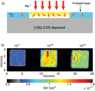
Next the sample was implanted with ions to create lattice vacancies. He+ implantation into a uniformly doped layer produces a uniform layer of NV centers with a controllable sensor thickness. The method also provides independent handles on both nitrogen and vacancy densities to optimize NV formation. This is impossible with N+ implantation alone where typically dozens of vacancies are created for every implanted N+ ion. Different areas of the sample were implanted with ion doses ranging from 109-1013 cm-3 at acceleration voltages of 15, 25, and 35 keV. After implanting, the sample was annealed at 850 ∘C for 1.5 hours in an Ar/H2 forming gas to allow the vacancies to diffuse and bind with the doped nitrogen in the lattice forming NV centers. A second 24 hour anneal at 450 ∘C in air was performed to convert NV centers from the neutral (NV0) to the negative (NV-) charge state Fu et al. (2010).
To characterize the NV- density, photoluminescence intensity from the implanted squares were compared to single NV centers in a control sample. The 2D density was calculated with the known excitation spot size and converted to a 3D density utilizing the 100 nm sensor thickness. As only the negatively-charged state of the NV center is useful for magnetic sensing, room temperature PL spectra were used to confirm the synthesized centers were in the desired charge state.
Before ion implantation and annealing, the density of centers formed during growth ranged from 0.7- cm-3 (average value ). The range in density is due to uneven incorporation of nitrogen during CVD growth which will be discussed further below. Fig. 1 shows an NV- density map of three squares implanted with , , and ions at 15 keV after annealing. Experimentally we found that for the three acceleration voltages varied by less than a factor of 2. This is consistent with SRIM calculations which show an average number of vacancies produced per ion of 30, 36, and 39, and an average ion range of 72, 112, and 135 nm, for 15, 25, and 35 keV acceleration voltages, respectively. All stopping ranges are within the 200 nm vacancy diffusion length Santori et al. (2009) of the doped 100 nm layer.
During the implantation process, the entire sample was exposed to an unknown radiation dose resulting in a background NV concentration of 0.1-1 cm-3. Squares implanted with ion doses of and cm-2 were indistinguishable from this background in most of the implanted areas. The optimal ion dose was 1012 cm-2 which resulted in an average of 11017 cm-3 corresponding to a 60-fold average increase over the unimplanted case. The obtained density is only one order of magnitude lower than the highest densities reported Acosta et al. (2009); Botsoa et al. (2011). These very high densities were obtained in high nitrogen doped (100 ppm) diamond which exhibit significantly broader resonance lines (2 MHz) Acosta et al. (2009) due to the N-NV dipolar coupling. Densities of cm-3 have also been obtained with N implantation and annealing Waxman et al. (2014) which also exhibited several MHz linewidths.
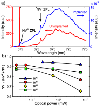
Room-temperature spectra comparing the NV- zero-phonon-line photoluminescence intensities for the implanted and unimplanted cases show a similar increase (40-fold) in NV density for the optimal implantation dose, as shown in Fig. 2a. Fig. 2b, shows the ratio of NV- to total NV (NV- + NV0) for different optical powers. The high ratio at low intensities indicate the NV is predominately in the desired charge state in the absence of optical excitation. The decrease in ratio with increased power is consistent with photoionization effects reported previously Manson and Harrison (2005).
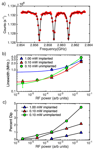
Next we measured the ODMR linewidth, , of the doped layer. Fig. 3a shows an optically detected magnetic resonance (ODMR) spectrum for the for one of the four NV crystal orientations. During the measurement, the NV centers are excited using a 532 nm continuous-wave laser while an RF field is swept through the electron spin resonance. Three dips are observed due to the hyperfine interaction of the NV electronic state with the 14N nucleus Acosta et al. (2009). To determine , the ODMR fluorescence spectra were fit to the sum of three Lorentzian functions of equal amplitude and , with a fixed 2.17 MHz hyperfine splitting.
Fig. 3b shows a plot of vs microwave power for the unimplanted and implanted conditions (15 keV, cm-2). The data is fit to the theoretical model where is the intrinsic dephasing rate, is the applied RF power, and a constant scaling to account for RF power broadening. The inhomogeneous spin relaxation time, , is determined from this fit. Experimentally we found that optical excitation powers below 100 W did not affect . No measurable difference in was found between the unimplanted and 15 keV implantation cases, which both exhibit T of 1.5 s ( 200 kHz). As little improvement in NV density was observed for higher implantation energies, detailed data on the effect of T for implantation energies greater than 15 keV were not taken.
The observed 200 kHz linewidth for our dense ensemble of NV centers is 2-5 times more narrow than ensembles created via e-irradiation in natural diamond with 1 ppm N Acosta et al. (2009, 2013), suggesting that there is a significant benefit in utilizing isotope purified 12C. The 200 kHz linewidth is, however, significantly broader than the 10 kHz inhomogeneous spread, due to the microscopic strain environment Rondin et al. (2014), between single NV centers grown in low nitrogen, 12C diamond Ishikawa et al. (2012). Given the minimal difference in T for unimplanted vs implanted conditions, we attribute the dominant dephasing mechanism to dipolar interactions between the NV centers and native nitrogen and/or between different NV centers.
Neglecting a small difference in g-factors between the NV and N Loubser and van Wyk (1978), we can obtain a rough estimate of the total density of paramagnetic impurities () by looking at the characteristic magnetic dipole coupling between two centers, Taylor et al. (2008). For a 200 kHz linewidth, we find an approximate density of 6. More detailed calculations taking into account NV interaction with the full N bath Wang and Takahashi (2013) indicate the conversion efficiency may be much higher. This numerical model found in which is the nitrogen density in ppm. Using this expression, we find a nitrogen concentration of 2. The average measured NV concentration for this implantation condition (15 keV, 10) was 1 cm-3. The conversion efficiency of N NV using He ion implantation thus ranges from 16 to 50%, with the main uncertainty due to the accuracy of the dipolar model. 50% is the maximum conversion for N, assuming the extra electron needed to obtain the negatively charged NV state comes from substitutional nitrogen donors Collins (2002). Finally, we note that EPR measurements indicate 0.2 to 0.5% of N incorporates as NV during -oriented CVD growth Edmonds et al. (2012), suggesting a 12-30% conversion efficiency for our process.
We now estimate the DC magnetic sensitivity of the engineered layer for a 1 second integration time. For a sensor biased at the steepest slope of the ODMR curve, the shot-noise magnetic sensitivity is given by Rondin et al. (2014)
| (3) |
in which is the detected photon count rate from the NV centers in the measurement pixel. For the case of continuous-wave (CW) RF and optical fields, the realized sensitivity is a complex interplay between optical and RF power. The optical excitation power has counteracting effects on , both increasing and (Fig. 3b). Similarly increasing the RF power will both increase and (Fig. 3c). For a 1 pixel, we find a sensitivity of nT at a 100 optical excitation intensity and an RF power corresponding to . This can be readily improved by a factor of utilizing a high-NA objective Jelezko and Wrachtrup (2006) and a further factor of 3 by driving all three hyperfine transitions simultaneously, resulting in a sensitivity of 30 nT.
The sensitivity can be further improved utilizing pulsed techniques. In this case we can decouple the optical excitation from the spin manipulation, enabling the use of high optical powers for spin readout without adversely affecting the ODMR linewidth. In this scheme, the optimal spin-manipulation time is Taylor et al. (2008), resulting in a time-averaged photon count rate of in Eq. 3, in which is the optical read-out pulse length Rondin et al. (2014). The pulsed sensitivity, identical to Eq. 1, is given by
| (4) |
Using reasonable parameters ( ns Rondin et al. (2014), , counts s-1 Jelezko and Wrachtrup (2006)) we estimate a sensitivity of .
In future sensor fabrication, improvements to the magnetic sensitivity could be realized by utilizing (111) surfaces to obtain a single orientation of NV centers () Michl et al. (2014); Lesik et al. (2014); Fukui et al. (2014). Additionally, optimizing the initial nitrogen density such that kHz could result in a further 10-fold decrease in the ODMR linewidth. More critically, however, is the need to further improve the uniformity of N incorporation during CVD growth. In this work, initial nitrogen incorporation densities varied by a factor of 3-4. Theoretically, in a calibrated, stable imaging system, this deviation should not pose a problem. Practically, however, spatial variations over time (e.g. due to vibrations or thermal drift) will result in a false magnetic signal. It has been recognized that nitrogen incorporation during diamond growth is extremely sensitive to the growth plane Samlenski et al. (1995); Miyazaki et al. (2014) and thus surface steps on a 100 surface. By reducing the misorientation of the surface cut (typically 1% in our samples), we expect to be able to enhance the incorporation homoneity. High NV spatial uniformity combined with the realized optical and spin properties presented in this work is expected to result in a high-sensitivity magnetic imaging system for magnetically-tagged biological applications and the study of optical-scale magnetic phenomena.
Acknowledgements This work has been supported by a University of Washington Molecular Engineering and Sciences Partnership grant. The work at Keio University has been supported by JSPS KAKENHI (S) No. 26220602 and Core-to-Core Program. VMA acknowledges support from NSF grant IIP-1549836. WDL was sponsored by NSF of China (Grant No. 61306123) and RGC of HKSAR (Grant No. 27205515). ZZ and WDL thank the facility support from Nanjing National Laboratory of Microstructures.
References
- Balasubramanian et al. (2008) G. Balasubramanian, I. Chan, R. Kolesov, M. Al-Hmoud, J. Tisler, C. Shin, C. Kim, A. Wojcik, P. R. Hemmer, A. Krueger, et al., Nature 455, 648 (2008).
- Maze et al. (2008) J. Maze, P. Stanwix, J. Hodges, S. Hong, J. Taylor, P. Cappellaro, L. Jiang, M. G. Dutt, E. Togan, A. Zibrov, et al., Nature 455, 644 (2008).
- Wolf et al. (2015) T. Wolf, P. Neumann, K. Nakamura, H. Sumiya, T. Ohshima, J. Isoya, and J. Wrachtrup, Phys. Rev. X 5, 041001 (2015).
- Steinert et al. (2010) S. Steinert, F. Dolde, P. Neumann, A. Aird, B. Naydenov, G. Balasubramanian, F. Jelezko, and J. Wrachtrup, Review of scientific instruments 81, 043705 (2010).
- Maertz et al. (2010) B. Maertz, A. Wijnheijmer, G. Fuchs, M. Nowakowski, and D. Awschalom, Applied Physics Letters 96, 092504 (2010).
- Pham et al. (2011) L. M. Pham, D. Le Sage, P. L. Stanwix, T. K. Yeung, D. Glenn, A. Trifonov, P. Cappellaro, P. Hemmer, M. D. Lukin, H. Park, et al., New Journal of Physics 13, 045021 (2011).
- Gould et al. (2014) M. Gould, R. J. Barbour, N. Thomas, H. Arami, K. M. Krishnan, and K.-M. C. Fu, Applied Physics Letters 105, 072406 (2014).
- Glenn et al. (2015) D. R. Glenn, K. Lee, H. Park, R. Weissleder, A. Yacoby, M. D. Lukin, H. Lee, R. L. Walsworth, and C. B. Connolly, Nature methods 12, 736 (2015).
- Rondin et al. (2014) L. Rondin, J. Tetienne, T. Hingant, J. Roch, P. Maletinsky, and V. Jacques, Reports on Progress in Physics 77, 056503 (2014).
- Budker and Romalis (2007) D. Budker and M. Romalis, Nature Physics 3, 227 (2007).
- Acosta et al. (2009) V. Acosta, E. Bauch, M. Ledbetter, C. Santori, K.-M. Fu, P. Barclay, R. Beausoleil, H. Linget, J. Roch, F. Treussart, et al., Physical Review B 80, 115202 (2009).
- Manson et al. (2006) N. Manson, J. Harrison, and M. Sellars, Physical Review B 74, 104303 (2006).
- Fang et al. (2013) K. Fang, V. M. Acosta, C. Santori, Z. Huang, K. M. Itoh, H. Watanabe, S. Shikata, and R. G. Beausoleil, Physical review letters 110, 130802 (2013).
- Wang and Takahashi (2013) Z.-H. Wang and S. Takahashi, Physical Review B 87, 115122 (2013).
- Taylor et al. (2008) J. Taylor, P. Cappellaro, L. Childress, L. Jiang, D. Budker, P. Hemmer, A. Yacoby, R. Walsworth, and M. Lukin, Nature Physics 4, 810 (2008).
- Kehayias et al. (2014) P. Kehayias, M. Mrózek, V. Acosta, A. Jarmola, D. Rudnicki, R. Folman, W. Gawlik, and D. Budker, Physical Review B 89, 245202 (2014).
- Ohashi et al. (2013) K. Ohashi, T. Rosskopf, H. Watanabe, M. Loretz, Y. Tao, R. Hauert, S. Tomizawa, T. Ishikawa, J. Ishi-Hayase, S. Shikata, C. Degen, and K. Itoh, Nano letters 13, 4733 (2013).
- Itoh and Watanabe (2014) K. Itoh and H. Watanabe, MRS Communications 4, 143 (2014).
- Ishikawa et al. (2012) T. Ishikawa, K.-M. C. Fu, C. Santori, V. M. Acosta, R. G. Beausoleil, H. Watanabe, S. Shikata, and K. M. Itoh, Nano letters 12, 2083 (2012).
- Fu et al. (2010) K.-M. Fu, C. Santori, P. Barclay, and R. Beausoleil, Applied Physics Letters 96, 121907 (2010).
- Santori et al. (2009) C. Santori, P. E. Barclay, K.-M. C. Fu, and R. G. Beausoleil, Physical Review B 79, 125313 (2009).
- Botsoa et al. (2011) J. Botsoa, T. Sauvage, M.-P. Adam, P. Desgardin, E. Leoni, B. Courtois, F. Treussart, and M.-F. Barthe, Physical Review B 84, 125209 (2011).
- Waxman et al. (2014) A. Waxman, Y. Schlussel, D. Groswasser, V. Acosta, L.-S. Bouchard, D. Budker, and R. Folman, Physical Review B 89, 054509 (2014).
- Manson and Harrison (2005) N. Manson and J. Harrison, Diamond and related materials 14, 1705 (2005).
- Davies and Crossfield (1973) G. Davies and M. Crossfield, Journal of Physics C: Solid State Physics 6, L104 (1973).
- Alkauskas et al. (2014) A. Alkauskas, B. B. Buckley, D. D. Awschalom, and C. G. Van de Walle, New Journal of Physics 16, 073026 (2014).
- Acosta et al. (2013) V. M. Acosta, K. Jensen, C. Santori, D. Budker, and R. G. Beausoleil, Physical review letters 110, 213605 (2013).
- Loubser and van Wyk (1978) J. Loubser and J. van Wyk, Reports on Progress in Physics 41, 1201 (1978).
- Collins (2002) A. T. Collins, Journal of Physics: Condensed Matter 14, 3743 (2002).
- Edmonds et al. (2012) A. Edmonds, U. D’Haenens-Johansson, R. Cruddace, M. Newton, K.-M. Fu, C. Santori, R. Beausoleil, D. Twitchen, and M. Markham, Physical Review B 86, 035201 (2012).
- Jelezko and Wrachtrup (2006) F. Jelezko and J. Wrachtrup, Physica Status Solidi A Applications And Materials Science 203, 3207 (2006).
- Michl et al. (2014) J. Michl, T. Teraji, S. Zaiser, I. Jakobi, G. Waldherr, F. Dolde, P. Neumann, M. W. Doherty, N. B. Manson, J. Isoya, et al., Applied Physics Letters 104, 102407 (2014).
- Lesik et al. (2014) M. Lesik, J.-P. Tetienne, A. Tallaire, J. Achard, V. Mille, A. Gicquel, J.-F. Roch, and V. Jacques, Applied Physics Letters 104, 113107 (2014).
- Fukui et al. (2014) T. Fukui, Y. Doi, T. Miyazaki, Y. Miyamoto, H. Kato, T. Matsumoto, T. Makino, S. Yamasaki, R. Morimoto, N. Tokuda, et al., Applied Physics Express 7, 055201 (2014).
- Samlenski et al. (1995) R. Samlenski, C. Haug, R. Brenn, C. Wild, R. Locher, and P. Koidl, Applied Physics Letters 67, 2798 (1995).
- Miyazaki et al. (2014) T. Miyazaki, Y. Miyamoto, T. Makino, H. Kato, S. Yamasaki, Y. Fukui, Y. Doi, N. Tokuda, M. Hatano, and N. Mizuochi, Applied Physics Letters 105, 261601 (2014).