Field-driven Mott gap collapse and resistive switch in correlated insulators
Abstract
Mott insulators are “unsuccessful metals” in which Coulomb repulsion prevents charge conduction despite a metal-like concentration of conduction electrons. The possibility to unlock the frozen carriers with an electric field offers tantalizing prospects of realizing new Mott-based microelectronic devices. Here we unveil how such unlocking happens in a simple model that shows coexistence of a stable Mott insulator and a metastable metal. Considering a slab subject to a linear potential drop we find, by means of Dynamical Mean-Field Theory that the electric breakdown of the Mott insulator occurs via a first-order insulator-to-metal transition characterized by an abrupt gap-collapse in sharp contrast to the standard Zener breakdown. The switch-on of conduction is due to the field-driven stabilization of the metastable metallic phase. Outside the region of insulator-metal coexistence, the electric breakdown occurs through a more conventional quantum tunneling across the Hubbard bands tilted by the field. Our findings rationalize recent experimental observations and may offer a guideline for future technological research.
Introduction.
The conventional description of the electric breakdown, i.e. the field driven formation of a conductive state in an otherwise insulating system, is based on the well-known Landau-Zener mechanism of quantum tunnelling across the insulating gap [1, 2]. However, the existence of a “rigid” band gap to be overcome by the field sets a lower bound of the threshold field and limits the density of excited carriers promoted across the gap. This ultimately leads to large density fluctuations at the nanoscale, one of the bottlenecks in device miniaturization [3]. These limitations are intrinsic in band insulators, whose gap is fixed as long as chemical composition and lattice structure do not change.
Because of the collective nature of their gap, Mott insulators have recently emerged as ideal candidates to overcome the above issues, providing a potential alternative to semiconductor-based microelectronics [3, 4]. The possibility of driving a gap closure in a Mott insulator by means of an electric field could enable to access a much larger carrier density than in semiconductors, potentially overcoming most limitations of conventional devices.
Experimental evidences for such an appealing field-driven resistive switch have been recently found in several Mott insulators [5, 6, 7, 8, 9, 10, 11, 12] and Mott-based devices [13, 14]. Remarkably, these experiments ubiquitously report a whole novel scenario for the electric breakdown that cannot be reconciled with the standard Landau-Zener description. For instance, the breakdown occurs through the abrupt formation of a conductive channel at anomalously small threshold fields [5], as opposed to the smooth activation at fields of the order of the gap as predicted by across-gap tunnelling. In addition, VO2 electric double layer transistors formed at a solid/electrolyte interface show massive conducting channels that suddenly open up above a threshold gate-voltage, with an extension much beyond the fundamental electrostatic screening length [13, 14].
While several mechanisms of resistive switch beyond the tunnelling paradigm are known, including thermally driven electric breakdown [15, 16], valence-change driven insulator-to-metal transitions [17, 18] and resistive transitions generated by the non-linear propagation of ionic defects [19], we believe that the above experiments still suggest another possible scenario of a genuine insulator-to-metal Mott transition triggered by the external field, as proposed in Refs. [5, 6] and modelled phenomenologically through a resistor network mimicking the competition between a stable insulating phase and a metastable metallic one. Nonetheless a true microscopic description in model Mott insulators is still lacking. Indeed, theoretical studies within the single-band Hubbard model, the paradigm of strongly correlated systems, have so far highlighted a breakdown that is essentially due to the tunnelling across the Mott gap, as if the latter were as rigid as the band gap in semiconductors [20, 21, 22, 23, 24]. Even if in some cases the tunnelling breakdown can be anticipated by the formation at large fields of in-gap states due to the Wannier-Stark effect [25, 26, 27], still the agreement with the above experiments remains poor.
Motivated by the strong evidence that the first-order character of the Mott transition plays a major role in the aforementioned experiments [5, 13, 6], in this Letter we explore the route to the electric breakdown that opens whenever a stable Mott insulator coexists with a metastable metal which is not connected to the insulating solution.
We realize this situation including extra degrees of freedom to the Hubbard model [28, 29], and we choose an orbital degree of freedom which is ubiquituously relevant in actual Mott insulating materials and increases the coexistence region with respect to the single-orbital model. In particular we consider the simplest modelling of a Mott insulator with a - gap [30], which we study in a slab geometry and in the presence of a constant electric field, i.e. an open circuit setup mimicking a FET [13] with a gate voltage but without source-drain bias.
We show that, within the insulator-metal coexistence region, an electric field can drive a discontinuous transition from the insulator to a gap-collapsed metal at threshold fields much smaller than those expected in a Zener breakdown.
Model.
We consider a half-filled two-orbital Hubbard model in a three dimensional lattice and in the presence of a crystal-field that lifts the orbital degeneracy. The generic Hamiltonian reads
| (1) |
where and are density operators at site . At and for not too large the model (2) describes a two band metal. At large the ground state is a non-magnetic Mott insulator, with one filled and one empty orbital. Such insulating state is stable against spin and/or orbital ordering due to the finite value of . This is in sharp contrast with the single-band Mott insulator description, in which the extensive spin entropy inevitably favors the onset of a magnetic order. Although the presence of a symmetry broken phase at weak or intermediate coupling in model (2) can not be excluded, its very existence and its properties critically depends on the model details. Therefore, to maintain the discussion as general as possible, in what follows we shall not account for possible broken symmetry phases [33].
In order not to weigh the Hamiltonian with too many parameters, we choose for our analysis the intra-orbital dispersion on a three-dimensional cubic lattice and a non-local hybridization that leaves the local single-particle density matrix diagonal in the orbital index even though the occupation of each orbital is not a conserved quantity. We observe that, because of our very specific choice, the model possesses an orbital U(1) symmetry that can be broken by a Stoner instability at weak coupling [34]. However, as we previously mentioned, we shall restrict our analysis only to the symmetry invariant subspace. The energy unit is such that the intra-orbital hopping is and we take . We solve the model by means of dynamical mean-field theory (DMFT) [2, 1] using an exact diagonalization solver (see Supplementary Materials).
Under the above assumptions, the model (2) undergoes a first-order Mott transition at a critical value of monotonically decreasing with increasing (see Fig.1(a)). For the sake of definiteness, in the following we fix the crystal-field splitting to , for which . For the insulating solution is stable, but the metal continues to exist as a metastable solution up to the spinodal point . The state variable that better characterizes the transition is the orbital polarization , i.e. the population imbalance between lower and upper orbital. At , the model describes a partially polarized metal (). A finite interaction reduces the effective bandwidth and induces a repulsion between occupied and unoccupied states, leading to an effective enhancement of the crystal field that increases the orbital polarization . At the first-order transition the metal turns abruptly into an almost fully polarized insulator () [35, 3], with a finite gap separating the occupied lowest band from the empty upper one [37]. A sort of Mott insulator “disguised” as a conventional band insulator.
In order to study the effect of an applied electric field we consider a layered slab of our idealized material subject to a static and uniform electric field (Coulomb gauge) directed along the slab direction (see Fig.1(b)), namely an open circuit configuration with playing the role of a gate voltage.
Results.
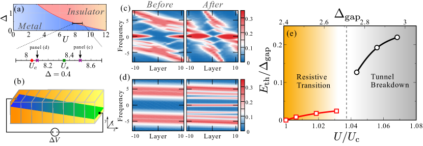
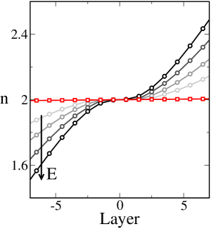
Starting from the equilibrium insulator at we increase the electric field and monitor the ground state evolution until, above a threshold value , a conducting state with a finite density of states at the Fermi level is established throughout the slab. We find that such field-induced conducting state has strikingly different properties depending whether the insulator at zero field is within the coexistence region, , or outside, . This is highlighted by panels (c)-(d) of Fig.1 showing the electric-field dependence of the layer resolved spectral density outside, panel (c), or inside, panel (d), the coexistence region. In both cases we show the spectra immediately before and after the formation of the conducting state.
Outside coexisistence, i.e. (panel c), we observe a marked tilting of lower (LHB) and upper (UHB) Hubbard bands, just as we would expect in a band insulator. When the field is large enough, the LHB crosses the Fermi energy at the left side of the slab, which is thus doped with holes, while the UHB does the same at the right side, which is instead doped with electrons. As a result, two facing and oppositely charged surface-layers with finite spectral weight at the Fermi level appear [37], whose thickness grows with the field until, above the threshold value , they touch in the center of the slab. Before touching, the two surface-layers are tunnel-coupled through an insulating barrier, the central part of the slab [37], and only above a sizeable density of states at the Fermi level is established throughout all the sample. We note that this behaviour is essentially that originally uncovered by Zener [1] in the Coulomb gauge, though here in an open circuit configuration, as already discussed in the case of Mott insulators [20, 41].
A completely different behaviour arises instead when the system is perturbed within the coexistence region between metal and insulator (). In this case a sharp insulator-to-metal transition instead takes place at the threshold field . This is illustrated by the abrupt change of the layer-resolved spectral density across the resistive transition reported in Fig. 1(d). As the threshold field is crossed, the gap abruptly collapses and a sizeable spectral weight at the Fermi level appears. The absence of any precursor on the insulating side indicates that the system displays a true resistive switch in which the ground state sharply changes from an insulator to a metal. As opposed to the previous case, the field-induced metal is homogeneous with a sizable spectral weight quite uniform throughout the whole slab [37].
In panel (e) we plot the threshold field in units of the zero-field insulating gap as a function of the distance from the first-order Mott transition. A clear break is observed in the curve around separating the two distinct regimes. The threshold field is small and slowly increasing within the coexistence region, while it gets larger and more steeply increasing outside. Remarkably, the strong variation of is in sharp contrast with the weak variation of the gap.
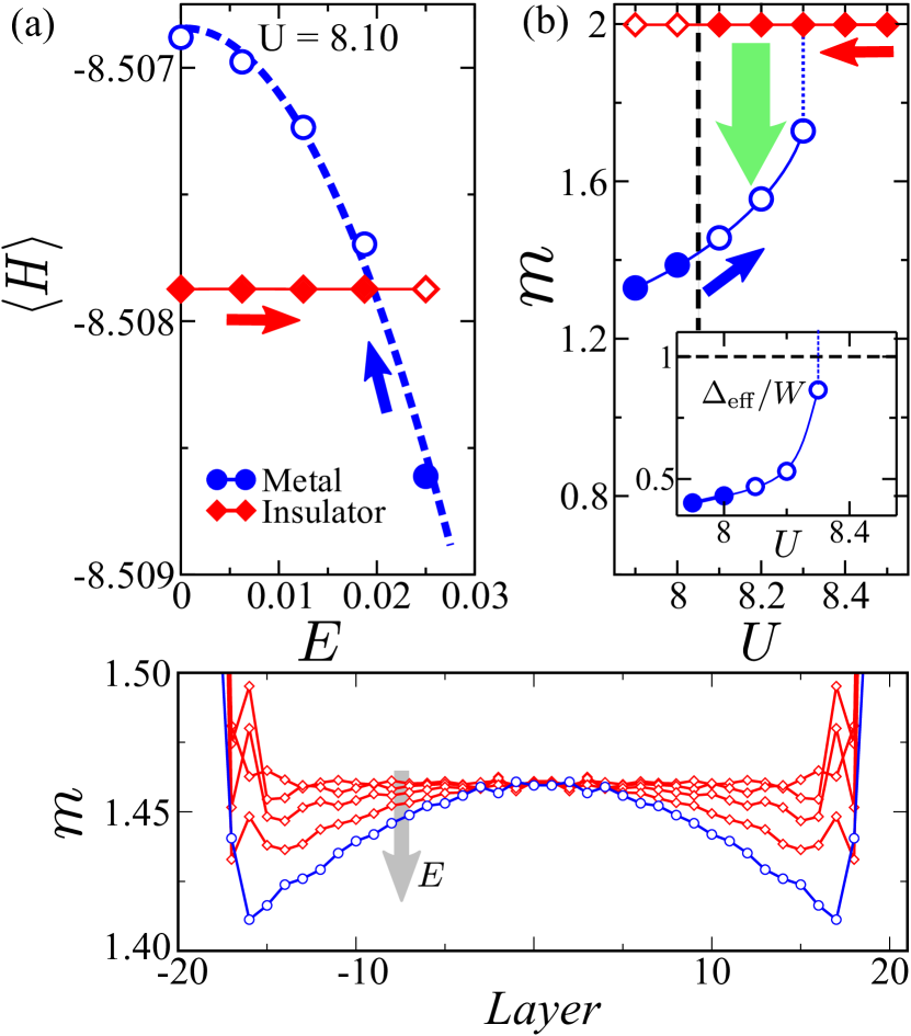
It is evident that the low-field resistive transition not extending beyond the spinodal point cannot be accidental. Indeed, as neatly shown in Fig. 2(a), the field-induced metallic phase is adiabatically connected with the metastable metal at zero field. At the insulating solution has lower internal energy and is separated from the metastable metal by a small energy difference. However, the metallic solution has a high electrical polarizability and it gains more energy from the field than the incompressible Mott insulator, whose energy remains essentially constant. As a consequence, the two energy curves eventually cross at the threshold field . The first-order character of such field-driven insulator-metal transition is further highlighted by the hysteresis loop of the equilibrium orbital polarization across the Mott transition, plotted in Fig. 2(b). The electric field thus acts as a switch between two phases with no adiabatic connection across the first-order metal-insulator transition [42].
Despite the field has the dramatic role of driving the first order insulator-metal transition, from the viewpoint of the metastable metal it is just a weak perturbation whose effects are accounted by linear response theory. Indeed, the energy of the metastable metal is well fitted with a simple parabola, see Fig. 2(a), as predicted by linear response theory, , where is the polarisability whose estimate is . This is important for what concerns the relevance of our results once the circuit were closed or a weak probing bias applied e.g. perpendicularly to the slab axis. Indeed, in the linear response regime we do not expect any prominent effect caused by a finite current flow [24] that could alter completely the physics with respect to the open circuit case.
In Fig.2(c) we show that, as long as the system is within the coexistence region (), the energy gain is accompanied by a significant reduction of the value of in the metastable metal, still in the linear response regime apart from finite size effects at the boundaries. This is remarkably since it appears without a strong charge redistribution across the sample [37]. In other words, the net effect of the electric field is essentially to decrease the orbital polarization of the metallic state, effectively moving in the phase diagram of Fig.1(e) as if or were reduced. In such a situation the threshold field depends only from the metal polarizability and we expect that it is remains constant as a function of the slab length until the potential at the boundaries becomes so large that non-linear effects appear so that coupling with iso-potential sources might become crucial to observe the same physics; an event we do not explore here.
Outside the coexistence region (), where a metastable metal no longer exists, the field modifies the insulating state through a strong charge redistribution, ultimately leading to the formation of the highly inhomogeneous conductive state in Fig. 1(c). The closure of the circuit in this case will induce more dramatic effects, even though we still expect the overall picture of a Landau-Zener tunnel breakdown to hold, possibly accompanied by other emergent effects [26, 27].
Conclusions.
The above results unveil a so far unexplored pathway to the metallisation of a correlated insulator, where the electric field drives a first-order transition from the insulator to a gap-collapsed metal phase, pre-existing as metastable state at zero field. Although the condition of being inside the insulator-metal coexistence region might be considered a rare circumstance in reality, we note that that observed Mott transitions are often characterised by quite wide hysteresis loops, see e.g. [43] in the popular case of V2O3.
Moreover, those results help clarifying why a similar phenomenon has not yet been observed, at least within DMFT, in the single-band Hubbard model, despite the latter also shows metal-insulator coexistence. In this model in the whole coexistence region the metal differs from the insulator only for the presence of a narrow quasiparticle peak at the Fermi level that hosts only a tiny percentage of carriers. For the same reason, the region of parameters where a stable insulator coexists with a metastable metal is extremely narrow, actually vanishing at zero temperature, so that one ends up observing always the same behaviour in a field as that of our model beyond the spinodal line [37].
Notwithstanding the obvious importance of the size of the coexistence domain on the insulating side of the Mott transition, we believe that the key issue to observe a genuine resistive switch is the competition of two neatly distinguishable phases, characterized by sharply different values of an extensive observable, in our case the orbital polarization , which can be tuned by the external field. In turn, this property might also be the rationale of the abrupt gap collapse at the resistive transition, which reflects the very nature of the gap [29]. In our Mott insulator model the gap separates two bands of different orbital character, i.e. it refers to the cost of redistributing electrons among the valence orbitals without changing valence, as opposed to the gap between lower and upper Hubbard bands in an idealized Mott insulator, which refers instead to the cost of changing the total charge within the valence shell.
A similar mechanism could be active in several known Mott insulators where the “polarization” of some degree of freedom starkly distinguishes the metal from the insulator. The physical nature of such observable can be material dependent – for instance in the case of VO2 [44, 45, 46] or V2O3 [47, 48] it is supposed to be the relative occupancy of two different -orbitals, much alike our simple case-study – yet the correlation-driven Mott transition would be associated to a sharp change of its value. In such context, the application of an external field would change this “polarization” favouring the metallic state and ultimately driving the resistive transition.
Acknowledgements.
We thank A. Georges, E. Janod, A. J. Millis, M.J. Rozenberg, for insightful discussions. A.A. and M.C. are financed by the European Union under FP7 ERC Starting Grant No. 240524 “SUPERBAD”. Part of this work was supported by European Union under the FP7 and H2020 Framework Programmes, Grant No. 280555 “GO FAST” and ERC Advanced Grant No. 692670 “FIRSTORM”, respectively. G.M. acknowledges support of the European Research Council (ERC-319286 “QMAC”).
References
- [1] Clarence Zener. A Theory of the Electrical Breakdown of Solid Dielectrics. Proceedings of the Royal Society of London A: Mathematical, Physical and Engineering Sciences, 145(855):523–529, 1934.
- [2] L. D. Landau. Zur Theorie der Energieubertragung. II. Phys. Z. Sowjetunion, 2:46, 1932.
- [3] D. M. Newns, J. A. Misewich, C. C. Tsuei, A Gupta, B. A. Scott, and A. Schrott. Mott transition field effect transistor. Applied Physics Letters, 73(6):780–782, 1998.
- [4] Hidenori Takagi and Harold Y. Hwang. An Emergent Change of Phase for Electronics. Science, 327(5973):1601–1602, 2010.
- [5] V. Guiot, L. Cario, E. Janod, B. Corraze, V. Ta Phuoc, M. Rozenberg, P. Stoliar, T. Cren, and D. Roditchev. Avalanche breakdown in GaTa4Se8narrow-gap Mott insulators. Nat. Commun., 4:1722, 04 2013.
- [6] Pablo Stoliar, Laurent Cario, Etiene Janod, Benoit Corraze, Catherine Guillot-Deudon, Sabrina Salmon-Bourmand, Vincent Guiot, Julien Tranchant, and Marcelo Rozenberg. Universal Electric-Field-Driven Resistive Transition in Narrow-Gap Mott Insulators. Advanced Materials, 25(23):3222–3226, 2013.
- [7] Jeehoon Kim, Changhyun Ko, Alex Frenzel, Shriram Ramanathan, and Jennifer E. Hoffman. Nanoscale imaging and control of resistance switching in VO2 at room temperature. Applied Physics Letters, 96(21), 2010.
- [8] Fumihiko Nakamura, Mariko Sakaki, Yuya Yamanaka, Sho Tamaru, Takashi Suzuki, and Yoshiteru Maeno. Electric-field-induced metal maintained by current of the Mott insulator Ca2RuO4. Scientific Reports, 3:2536 EP–, 08 2013.
- [9] A. A. Fursina, R. G. S. Sofin, I. V. Shvets, and D. Natelson. Origin of hysteresis in resistive switching in magnetite is Joule heating. Phys. Rev. B, 79:245131, Jun 2009.
- [10] A A Fursina, R G S Sofin, I V Shvets, and D Natelson. Statistical distribution of the electric field-driven switching of the Verwey state in Fe 3 O 4. New Journal of Physics, 14(1):013019, 2012.
- [11] S. Guénon, S. Scharinger, Siming Wang, J. G. Ramírez, D. Koelle, R. Kleiner, and Ivan K. Schuller. Electrical breakdown in a V 2 O 3 device at the insulator-to-metal transition. EPL (Europhysics Letters), 101(5):57003, 2013.
- [12] Etienne Janod, Julien Tranchant, Benoit Corraze, Madec Querré, Pablo Stoliar, Marcelo Rozenberg, Tristan Cren, Dimitri Roditchev, Vinh Ta Phuoc, Marie-Paule Besland, and Laurent Cario. Resistive Switching in Mott Insulators and Correlated Systems. Advanced Functional Materials, 25(40):6287–6305, 2015.
- [13] M. Nakano, K. Shibuya, D. Okuyama, T. Hatano, S. Ono, M. Kawasaki, Y. Iwasa, and Y. Tokura. Collective bulk carrier delocalization driven by electrostatic surface charge accumulation. Nature, 487:459–462, July 2012.
- [14] D. Okuyama, M. Nakano, S. Takeshita, H. Ohsumi, S. Tardif, K. Shibuya, T. Hatano, H. Yumoto, T. Koyama, H. Ohashi, M. Takata, M. Kawasaki, T. Arima, Y. Tokura, and Y. Iwasa. Gate-tunable gigantic lattice deformation in VO2. Applied Physics Letters, 104(2):023507, 2014.
- [15] A. Zimmers, L. Aigouy, M. Mortier, A. Sharoni, Siming Wang, K. G. West, J. G. Ramirez, and Ivan K. Schuller. Role of Thermal Heating on the Voltage Induced Insulator-Metal Transition in . Phys. Rev. Lett., 110:056601, Jan 2013.
- [16] Justin S. Brockman, Li Gao, Brian Hughes, Charles T. Rettner, Mahesh G. Samant, Kevin P. Roche, and ParkinStuart S. P. Subnanosecond incubation times for electric-field-induced metallization of a correlated electron oxide. Nat Nano, 9(6):453–458, 06 2014.
- [17] Hidekazu Shimotani, Hirotaka Suzuki, Kazunori Ueno, Masashi Kawasaki, and Yoshihiro Iwasa. p-type field-effect transistor of nio with electric double-layer gating. Applied Physics Letters, 92(24):–, 2008.
- [18] Sang-Yun Sung, Se-Yun Kim, Kwang-Min Jo, Joon-Hyung Lee, Jeong-Joo Kim, Sang-Gon Kim, Kyoung-Hoon Chai, S. J. Pearton, D. P. Norton, and Young-Woo Heo. Fabrication of p-channel thin-film transistors using cuo active layers deposited at low temperature. Applied Physics Letters, 97(22):–, 2010.
- [19] Shao Tang, Federico Tesler, Fernando Gomez Marlasca, Pablo Levy, V. Dobrosavljević, and Marcelo Rozenberg. Shock waves and commutation speed of memristors. Phys. Rev. X, 6:011028, Mar 2016.
- [20] Takashi Oka, Ryotaro Arita, and Hideo Aoki. Breakdown of a Mott Insulator: A Nonadiabatic Tunneling Mechanism. Phys. Rev. Lett., 91:066406, Aug 2003.
- [21] Satoshi Okamoto. Nonlinear Transport through Strongly Correlated Two-Terminal Heterostructures: A Dynamical Mean-Field Approach. Phys. Rev. Lett., 101:116807, Sep 2008.
- [22] Martin Eckstein, Takashi Oka, and Philipp Werner. Dielectric Breakdown of Mott Insulators in Dynamical Mean-Field Theory. Phys. Rev. Lett., 105:146404, Sep 2010.
- [23] Jiajun Li, Camille Aron, Gabriel Kotliar, and Jong E. Han. Electric-field-driven resistive switching in the dissipative hubbard model. Phys. Rev. Lett., 114:226403, Jun 2015.
- [24] G. Mazza, A. Amaricci, M. Capone, and M. Fabrizio. Electronic transport and dynamics in correlated heterostructures. Phys. Rev. B, 91:195124, May 2015.
- [25] A. V. Joura, J. K. Freericks, and Th. Pruschke. Steady-state nonequilibrium density of states of driven strongly correlated lattice models in infinite dimensions. Phys. Rev. Lett., 101:196401, Nov 2008.
- [26] N Tsuji, T Oka, and H Aoki. Correlated electron systems periodically driven out of equilibrium: Floquet + DMFT formalism. Phys. Rev. B, 78(23):235124, 2008.
- [27] Woo-Ram Lee and Kwon Park. Dielectric breakdown via emergent nonequilibrium steady states of the electric-field-driven mott insulator. Phys. Rev. B, 89:205126, May 2014.
- [28] Isao H. Inoue and Marcelo J. Rozenberg. Taming the Mott Transition for a Novel Mott Transistor. Advanced Functional Materials, 18(16):2289–2292, 2008.
- [29] Matteo Sandri and Michele Fabrizio. Nonequilibrium gap collapse near a first-order Mott transition. Phys. Rev. B, 91:115102, Mar 2015.
- [30] J. Zaanen, G. A. Sawatzky, and J. W. Allen. Band gaps and electronic structure of transition-metal compounds. Phys. Rev. Lett., 55:418–421, Jul 1985.
- [31] Antoine Georges, Gabriel Kotliar, Werner Krauth, and Marcelo J. Rozenberg. Dynamical mean-field theory of strongly correlated fermion systems and the limit of infinite dimensions. Rev. Mod. Phys., 68:13, 1996.
- [32] M. Potthoff and W. Nolting. Surface metal-insulator transition in the Hubbard model. Phys. Rev. B, 59:2549–2555, Jan 1999.
- [33] Jiajun Li, Camille Aron, Gabriel Kotliar, and Jong E. Han. Resistive Switching via Filament Formation in Bias-Driven Correlated Insulators. arXiv:1608.01931 (2016)
- [34] D. Golež, P. Werner and M. Eckstein Photoinduced gap closure in an excitonic insulator Phys. Rev. B 94:035121, Jul 2016.
- [35] Philipp Werner and Andrew J. Millis. High-Spin to Low-Spin and Orbital Polarization Transitions in Multiorbital Mott Systems. Phys. Rev. Lett., 99:126405, Sep 2007.
- [36] Alexander I. Poteryaev, Michel Ferrero, Antoine Georges, and Olivier Parcollet. Effect of crystal-field splitting and interband hybridization on the metal-insulator transitions of strongly correlated systems. Phys. Rev. B, 78:045115, 2008.
- [37] See Supplementary Material which includes Refs. [2, 3, 38, 4, 40]
- [38] Cornelius Lanczos. An iteration method for the solution of the eigenvalue problem of linear differential and integral operators. Journal of Research of the National Bureau of Standards, 45, 4 (1950).
- [39] Giovannni Borghi, Michele Fabrizio and Erio Tosatti. Strongly correlated metal interfaces in the Gutzwiller approximation Phys. Rev. B, 81, 115134 (2010).
- [40] Philipp Werner and Andrew J. Millis. Doping-driven Mott transition in the one-band Hubbard model Phys. Rev. B, 75, 085108 (2007).
- [41] B. Mayer, C. Schmidt, A. Grupp, J. Bühler, J. Oelmann, R. E. Marvel, R. F. Haglund, T. Oka, D. Brida, A. Leitenstorfer, and A. Pashkin. Tunneling breakdown of a strongly correlated insulating state in induced by intense multiterahertz excitation. Phys. Rev. B, 91:235113, Jun 2015.
- [42] A. Camjayi, C. Acha, R. Weht, M.G̃. Rodríguez, B. Corraze, E. Janod, L. Cario, and M.J̃. Rozenberg. First-Order Insulator-to-Metal Mott Transition in the Paramagnetic 3D System . Phys. Rev. Lett., 113:086404, Aug 2014.
- [43] P. Limelette, A. Georges, D. Jérome, P. Wzietek, P. Metcalf, and J. M. Honig. Universality and critical behavior at the mott transition. Science, 302(5642):89–92, 2003.
- [44] John B. Goodenough. The two components of the crystallographic transition in vo2. Journal of Solid State Chemistry, 3(4):490 – 500, 1971.
- [45] V. Eyert. The metal-insulator transitions of vo2: A band theoretical approach. Annalen der Physik, 11(9):650–704, 2002.
- [46] S. Biermann, A. Poteryaev, A. I. Lichtenstein, and A. Georges. Dynamical Singlets and Correlation-Assisted Peierls Transition in . Phys. Rev. Lett., 94:026404, Jan 2005.
- [47] Alexander I. Poteryaev, Jan M. Tomczak, Silke Biermann, Antoine Georges, Alexander I. Lichtenstein, Alexey N. Rubtsov, Tanusri Saha-Dasgupta, and Ole K. Andersen. Enhanced crystal-field splitting and orbital-selective coherence induced by strong correlations in . Phys. Rev. B, 76:085127, Aug 2007.
- [48] Daniel Grieger and Michele Fabrizio. Low-temperature magnetic ordering and structural distortions in vanadium sesquioxide . Phys. Rev. B, 92:075121, Aug 2015.
Supplementary Informations:
Field-driven Mott gap collapse and resistive switch in correlated insulators
G. Mazza, A. Amaricci, M. Capone and M. Fabrizio
I Model and Method
We consider the following two-bands model Hamiltonian:
| (2) |
where and , while is the intra-band dispersion on a three-dimensional cubic lattice. We also add a non-local hybridization which allows for inter-orbital charge fluctuations but leaves the local single-particle density matrix diagonal in the orbital index. We set the energy unit such that the hopping , the hybridization .
In addition we consider a constant electric field directed along the -axis: . Working in the Coulomb gauge we express the electric field in terms of a linearly varying potential:
| (3) |
and we assume that the field is imposed on a system with finite extension along the -direction, mimicking a sample between two external leads kept at finite voltage difference . To this extent we introduce a three-dimensional layered structure (Fig. 1(b) main text) and fix the reference potential value imposing a symmetric voltage drop respect to its center:
| (4) |
The Hamiltonian for the slab structure is obtained performing a discrete Fourier transform along the direction of the fermionic operators defined in momentum space
| (5) |
where the explicit form of the basis functions takes into account the open boundary conditions which we impose on the system. Using a vector representation for the orbitals fermionic operators: and setting to unity the elementary charge we obtain
| (6) |
where is the crystal-field splitting, is the local Coulomb interaction strength, is the scalar potential defined by Eq. 4 and the matrices and contain respectively the intra- and inter- layer hopping amplitudes
| (7) |
The model is solved using the extension of the DMFT formalism to in-homogeneous systems [1], based on the assumption that the self-energies encoding the effect of all the many-body correlation are completely local in space while retaining an explicit dependence on the layer index
| (8) |
Following the standard DMFT approach, the layer-dependent self-energies are then extracted from a set of layer-dependent single-site effective problems to be self-consistently determined imposing that the lattice local Green’s function computed using such local self-energy is equal to the Green’s function of the effective single-site problem. Indicating with the bare propagators of the effective single-sites problems, the problem is practically solved using the following equations which implicitly relate and
| (9) |
| (10) |
where we indicate with the matrix constructed with all the matrices. In the present case we map the effective single-sites problems onto interacting Anderson impurity models which we solve using a finite bath discretization and an Exact Diagonalization scheme based on the Lanczos method [2].
II Zero-bias Mott transition
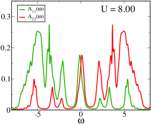
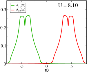
In this section we provide few additional information concerning the zero bias metal-insulator transition. As described in the main text the transition is driven by the combined effects of the interaction enhancement of the polarization strenght and the shrinking of the coherent quasiparticle peak. As a consequence, the Mott transition appears as a sharp charge redistribution between the two orbitals. We show this plotting in Fig. 1(a) the orbital-resolved spectral functions for two values of the interaction parameter just before and after the metal-insulator critical value . For the two spectral functions overlap with a sizable spectral weight at the Fermi level displaying a two-orbitals character. The abrupt separation of the orbital resolved spectral weight occours for leading to a Mott insulator in which the lower band is fully occupied and the upper one empty (panel b Fig. 1). We notice that due to the finite hybridization in the kinetic part of the Hamiltonian the orbital polarization is not exaclty complete with less than one percent residual occupation in the upper orbital [3].
III Resistive- Vs. tunnel-like formation of the metallic states
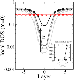
A more exhaustive description of the sharp differences between the resistive- and the tunnel-breakdown described in the main text can be appreciated looking at the layer distributions of the charge density and of the bias-induced spectral density at the Fermi (see Fig. 1(b)).
In the case of the resistive switch, namely the insulator-to-metal transition followed by the abrupt Mott gap collapse close to the Mott transition, we observe an infinitesimal tilting of the charge distribution (red squares in Fig. 2(b) left) and an homogenous distribution of the spectral weight (red squares in Fig. 2(b) right).
On the contrary far away from the Mott transition, as expected by the strong tilting of the layer-resolved spectral density (main text), a very strong charge redistribution is needed in order to observe the formation of conducting states (gray to black circles in Fig. 2(b) left). This leads to the gradual formation of two metallic regions at the boundaries which are separated by a bulk region in which the spectral weight results exponentially suppressed (gray to black circles in Fig. 2(b) right). Such evanescent spectral weight represents the tunnel through the bulk Mott insulating region of the carriers from the two doped metallic regions at the slab boundaries [4]. This confirms the tunnel-like scenario for the field-induced formation of conducting paths deep in the Mott insulating phase (Fig.1e in the main text). In the inset we show the field evolution of the spectral density at the Fermi level for the bulk layer. The spectral density increases linearly up to a threshold value where a clear jump is observed signaling the disappearence of the bulk insulating region. We take this value to extract the breakdown threshold field for reported in the main text.
References
- [1] M. Potthoff and W. Nolting. Phys. Rev. B, 59, 2549–2555 (1999).
- [2] A. Georges, G. Kotliar, W. Krauth, and M. J. Rozenberg. Rev. Mod. Phys., 68, 13 (1996).
- [3] A. I. Poteryaev, M. Ferrero, A. Georges, and O. Parcollet. Phys. Rev. B, 78, 045115 (2008).
- [4] G. Borghi, M. Fabrizio and E. Tosatti. Phys. Rev. B, 81, 115134 (2010).