Photonic realization of topologically protected bound states in domain-wall waveguide arrays
Abstract
We present an analytical theory of topologically protected photonic states for the two-dimensional Maxwell equations for a class of continuous periodic dielectric structures, modulated by a domain wall. We further numerically confirm the applicability of this theory for three-dimensional structures.
I Introduction
Due to their role as vehicles for localization and transport of energy, surface modes have long been recognized to be of central importance Tamm (1932); Shockley (1939). A striking example is that of topologically protected edge states, which were first studied in the quantum Hall effect in condensed matter physics Halperin (1982); Wen (1991); Thouless et al. (1982). Since 2005, there has been intense focus on the protected states of topological insulators Kane and Mele (2005); Hasan and Kane (2010). More recently, there has also been growing interest in photonic analogues of the topologically protected states observed in electronic systems Raghu and Haldane (2008); Haldane and Raghu (2008); Lu et al. (2014). In particular, such states have been shown to arise via line-defects (edges) and time-reversal or spatial-inversion symmetry breaking in linear and nonlinear photonics, e.g. Raghu and Haldane (2008); Haldane and Raghu (2008); Wang et al. (2008); Joannopoulos et al. (2008); Plotnik et al. (2014); Lu et al. (2013); Kocaman et al. (2011, 2009); Jiao et al. (2006).
Theoretical arguments for the existence and robustness of topologically protected edge states have been given in terms of topological invariants associated with the band structure, e.g. Chern index or Zak phase backed by numerical simulations. A systematic justification of the applicability of such invariants, however, appears only to have been provided in tight-binding models, e.g. Delplace et al. (2011); Mong and Shivamoggi (2011); Graf and Porta (2013); Chiu et al. (2015). In the photonic setting, this corresponds to the limit of infinite medium contrast. We seek a general understanding of topological protection, a theory which is applicable outside of limiting regimes, such as the tight-binding or nearly-free-photon approximations. Indeed, many physical settings of interest, including photonics in low contrast periodic structures, fall outside these regimes; see also Plotnik et al. (2014).
In Fefferman et al. (2014, 2016), a class of one-dimensional (1D) continuous systems described by the Schrödinger equation with a domain-wall modulated (DWM) periodic potential were proved to have topologically protected bound states, originating in the zero-mode of an effective 1D Dirac equation, a mechanism which plays a role in Su et al. (1979); Raghu and Haldane (2008); see also Jackiw and Rebbi (1976). In this Letter, we propose and investigate a photonic realization of these states as topologically protected guided wave modes in a class of coupled two-dimensional (2D) waveguide arrays governed by Maxwell’s equations. No tight-binding or nearly-free-photon assumptions are made; the results hold for bulk structures of arbitrary material contrast.
We further demonstrate, through ab initio numerical simulations for the full three-dimensional (3D) Maxwell equations, that these waveguide modes and their properties persist for physically realistic 3D optical waveguide arrays. In particular, robustness against geometric and intrinsic background thermal perturbations is demonstrated. These states have fundamentally linear dispersion and broadband flat group velocity dispersion.
Photonic waveguide array structures are an important class of photonic crystals, providing a natural platform for basic studies of topological insulators and their photonic applications. They permit qualitative study and quantitative measurements of many phenomena Bromberg et al. (2009); Joglekar et al. (2013). Recent work has explored 2D arrays in linear and nonlinear regimes, in both deterministic and random media Khanikaev et al. (2013); Rechtsman et al. (2013a); Ma et al. (2015); Titum et al. ; Zeuner et al. (2014); Rechtsman et al. (2013b); Lumer et al. (2013).
II Schrödinger setting
II.1 Guided TM Maxwell modes as eigenmodes of the Schrödinger equation
The propagation of light in space, with coordinates , in a dielectric medium with constant permeability and permittivity depending on only one variable, , is governed by Maxwell’s equations. Time-harmonic modes, which propagate in the -waveguided direction are of transverse-electric (TE) or transverse-magnetic (TM) type. We focus on the TM case; an analogous discussion holds for TE modes.
TM modes with frequency , which are localized in the transverse direction, are of the form
| (1) |
where is a solution of the Schrödinger eigenvalue problem (EVP) with potential , and energy :
| (2) |
Here, denotes the guided mode effective permittivity as a function of the dimensionless transverse distance , is the -propagation constant, and is the vacuum speed of light. If is an eigenpair of (2) for which , then is real and (1) is a guided TM mode, propagating in and localized in .
II.2 Topologically protected bound states
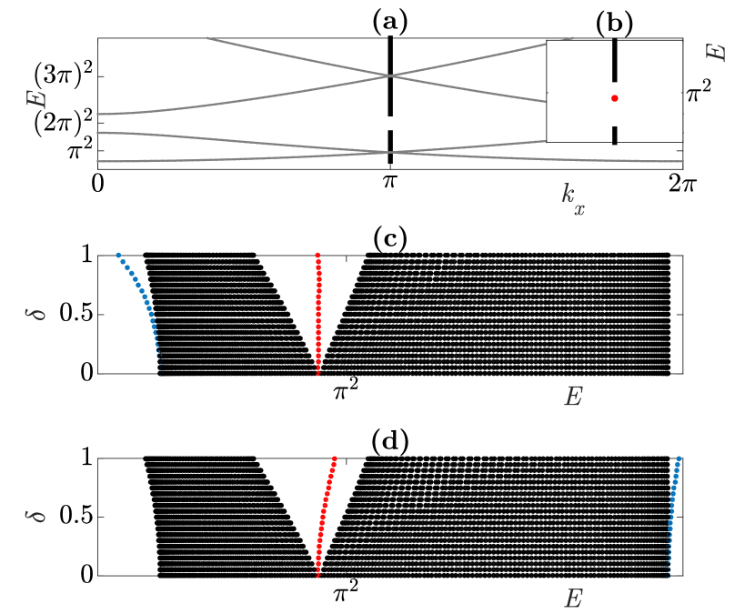
In Fefferman et al. (2014, 2016), the authors study topologically protected bound states in 1D domain-wall modulated (DWM) Schrödinger Hamiltonians of the form: where and denote even-index and odd-index cosine series, respectively; and is a so-called domain wall function that satisfies , with . interpolates between dimer structures at . For , has distinguished quasimomentum-energy pairs where its dispersion curves cross linearly; see FIG. 1(a).
Theorem 1 (Fefferman et al. (2014, 2016))
The Floquet-Bloch EVPs for : , , parametrized by , possess Dirac points. These are pairs with mappings such that the dispersion locus near is given by: Here, is the “Fermi velocity”.
Associated with each Dirac point of the periodic (unmodulated) Hamiltonian, , there is a topologically protected branch of bound states of the Schrödinger EVP for the DWM Hamiltonian, .
Theorem 2 (Fefferman et al. (2014, 2016))
Let denote a Dirac point of . Assume the (generically satisfied) non-degeneracy condition: , where and .
-
1.
There exists, for small , a family of exponentially localized eigensolutions, of the EVP: , bifurcating from energy at .
-
2.
is well-approximated by a slowly varying and spatially decaying modulation of the degenerate modes and : . The amplitude vector, , is a zero mode of a 1D Dirac operator: , where and are the standard Pauli matrices.
-
3.
This zero-energy state of persists for arbitrary spatially localized perturbations of the domain wall, , and hence the bifurcation is topologically protected.
II.3 Protected vs non-protected modes
To contrast the protected modes of DWM structures with conventional non-protected modes of periodic structures with defects which arise via bifurcations from a band-edge energy, , consider the Hamiltonian , which incorporates both a domain-wall induced phase defect () and a localized defect (); scalings are chosen so that both effects are of comparable size. Band-edge bifurcations are seeded by bound states of the effective Schrödinger operator: , with effective mass Kittel (1996) and effective potential , . While the zero-energy eigenstate of , which induces the bifurcation of bound states from a Dirac point Shockley (1939), persists under arbitrary (even large) localized perturbations of the domain wall, , the localized states of , and therefore their induced branch of bound states Tamm (1932), are not stable to arbitrary localized perturbations, Hoefer and Weinstein (2011); Duchêne et al. (2015).
In FIG. 1(c), where , the domain wall induces bifurcations from Dirac points as well as from band edges. In FIG. 1(d), a non-zero localized perturbation, , has destroyed the lower band edge bifurcation; the edge bifurcation can be removed by smooth deformation of while the Dirac point bifurcation is topologically protected.
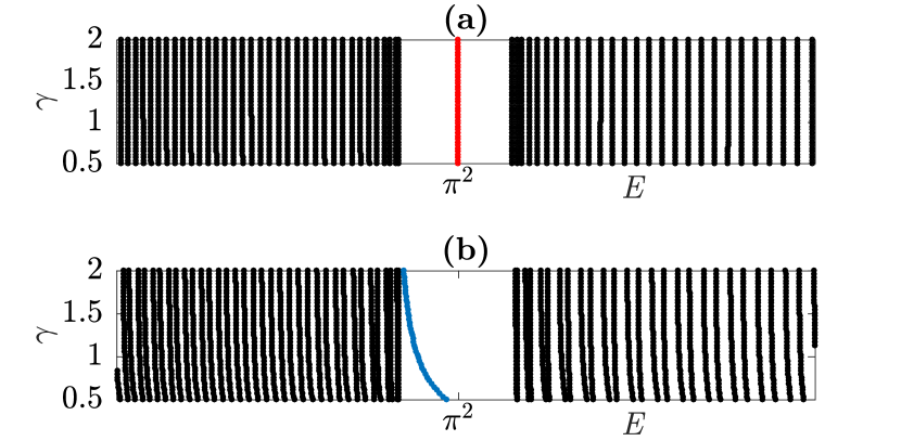
The protected states of DWM structures also exhibit a remarkable robustness of their eigenvalues (operating or working frequencies) when compared with those of conventional structures with localized defects. To illustrate this, we extend the previous model to a Hamiltonian , with defect mode eigenvalue, , where changing varies the phase defect’s transition region width (where transitions between positive to negative values) and the area of the localized defect, . The potential in is assumed to be smooth. For and , is of the order for the protected mode (DWM , ), and of the order for the non-protected mode (, localized ).
For , we have ; see Theorem 2 and Duchêne et al. (2015); Fefferman et al. (2014). Therefore, using the rapid oscillations of , we have , for all where . On the other hand, a direct computation gives . Hence, for small and , we have . Numerical simulations for larger and further corroborate the strong robustness of the operating frequency of topologically protected modes; see FIG. 2.
III Maxwell setting
III.1 2D topologically protected, guided TM modes
Corollary 1
Maxwell’s equations exhibit topologically protected, transversely localized, guided TM modes.
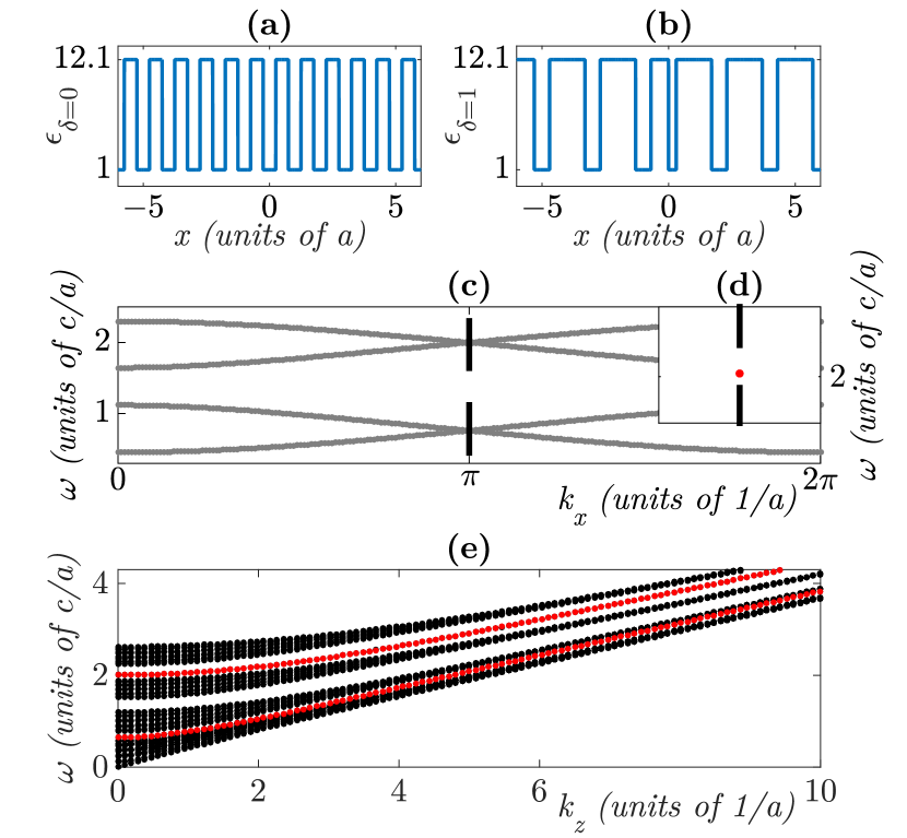
We realize these topologically robust TM modes in a photonic waveguide array by constructing a coupled 2D silicon-air waveguide array profile, , corresponding to a potential, . We construct to be the two-valued approximation of a choice of , scaled to match the effective permittivities of silicon () and air (). is the DWM structure and is the periodic potential having Dirac points. Finally, we set ; see (2). The 2D DWM waveguide array is shown in FIG. 3(b). Although the relative length scale between and is important, the computations may be carried out at arbitrary length scales due to the scale invariance of Maxwell’s equations Joannopoulos et al. (2008).
Since the numerically computed lowest energy gap mode of the Schrödinger equation with the DWM potential, , satisfies , is real and the corresponding TM mode in (1) is guided.
The dispersion curves, , for TM modes of the 2D periodic (unmodulated) structure, , are displayed in FIG. 3(c). These curves are computed by solving the 2D Maxwell equations for at discrete values, using MPB Johnson and Joannopoulos (2001). The dispersion curves, , for the DWM waveguide, , are displayed in FIG. 3(e). In analogy with the Schrödinger setting, robust guided-modes are observed in gaps about Dirac points at quasi-momentum , where is the lattice constant; see FIG. 1(a)-(b). Qualitatively similar dispersion curves are observed for TE modes.
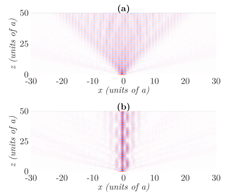
We numerically study on-axis -propagation in the DWM 2D waveguide of a Gaussian wave-packet, using the approximate paraxial Schrödinger equation Lifante (2003); Kawano and Kitoh (2004). For the periodic array, the energy of the launched packet quickly delocalizes (FIG. 4(a)). In contrast, in the DWM structure, a topologically protected mode is excited and confines most of the energy on-axis (FIG. 4(b)). A quantitative comparison of localization properties of the DWM and periodic structures is obtained by measuring, , the fraction of power remaining within (roughly) the width of the profile of the stationary localized mode of the DWM structure at : . The DWM structure achieves significantly more localization: .
III.2 3D topologically protected, guided TM modes
The theory summarized in Theorem 2 and Corollary 1 is exact and rigorous for a 2D waveguide with effective permittivity satisfying . The physical 3D DWM waveguide is a finite height () truncation of the 2D structure. Numerical simulations (below) show a long lived 3D state, localized in the -direction even for small height truncations. A schematic of a 3D silicon waveguide (effective permittivity ) with height and silicon-dioxide cladding (effective permittivity ) is shown in FIG. 5(b).
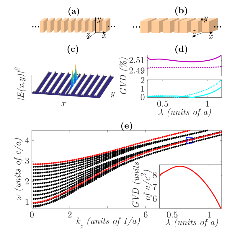
Numerically computed dispersion curves: , for TM modes of the 3D DWM waveguide are displayed in FIG. 5(e). From , we compute the group velocity dispersion (GVD), ; see figure inset.
Corollary 1 ensures that the 2D TM-modes, which bifurcate from Dirac points, are topologically stable. We confirm the existence and persistence of their 3D counterparts through a computational study of two classes of physical perturbations: (i) changes in the effective permittivity due to thermal fluctuations; and (ii) geometric perturbations in the lattice constants (waveguide channels) of the array due to fabrication imperfections, both perturbations, randomly sampled from a uniform distribution. FIG. 5(d) (solid) displays the mean deviation of the GVD curves of perturbed waveguides relative to the unperturbed (DWM) waveguide, calculated from one hundred independent simulations. Also plotted (dotted), for reference, are the corresponding mean relative deviation of the GVD curves for a regular channel silicon-silicon dioxide waveguide (of height and channel width ). GVD robustness of topologically protected DWM guided modes, with respect to thermal and geometric perturbations, is comparable to that for regular channel modes.
Fixing , we also observe that the mode itself remains localized against the perturbations, as measured by the perturbed effective mode area statistics Agrawal (2007): Here the perturbed mode areas are normalized against the unperturbed mode area, and reported as means with corresponding standard deviations, calculated from fifty independent simulations.
IV Conclusion
Summarizing, building upon the theory of Fefferman et al. (2014, 2016), we have demonstrated the bifurcation of highly robust guided TM modes for Maxwell’s equations governing a class of DWM photonic waveguide arrays in 2D. Our findings are corroborated by full Maxwell simulations of physically realistic 3D structures, derived from our 2D model. In contrast to the guided wave modes of conventional waveguides, DWM modes are robust to large localized perturbations while having comparable GVD robustness characteristics. These topologically protected states may be well-suited for chip-scale nanofabrication of semiconductor waveguides for communications and frequency source generation.
Acknowledgements.
The authors thank C. Wilson and M. Spiegelman at Columbia LDEO for providing valuable computing resources, E. D. Kinigstein and J. F. McMillan for helpful discussions, and the referees for many stimulating insightful comments. This work was supported, in part, by NSF Grants DMS-1265524 (C.L.F.), DMS-1008855 and DMS-1412560 (J.P.L.-T., M.I.W.), CMMI-1520952 (C.W.W., J.Y.), (IGERT) DGE-1069420 (J.P.L.-T., M.I.W., C.W.W., J.Y.); ONR Grant N00014-14-1-0041 (C.W.W., J.Y.); and the Simons Foundation Grant 376319 (M.I.W.).References
- Tamm (1932) I. Tamm, Phys. Z. Sowjetunion 1, 733 (1932).
- Shockley (1939) W. Shockley, Physical review 56, 317 (1939).
- Halperin (1982) B. I. Halperin, Physical Review B 25, 2185 (1982).
- Wen (1991) X.-G. Wen, Physical Review B 43, 11025 (1991).
- Thouless et al. (1982) D. J. Thouless, M. Kohmoto, M. P. Nightingale, and M. denNijs, Phys. Rev. Lett. 49, 405 (1982).
- Kane and Mele (2005) C. L. Kane and E. J. Mele, Phys. Rev. Lett. 95, 146802 (2005).
- Hasan and Kane (2010) M. Z. Hasan and C. L. Kane, Reviews of Modern Physics 82, 3045 (2010).
- Raghu and Haldane (2008) S. Raghu and F. D. M. Haldane, Physical Review A 78, 033834 (2008).
- Haldane and Raghu (2008) F. D. M. Haldane and S. Raghu, Phys. Rev. Lett. 100, 013904 (2008).
- Lu et al. (2014) L. Lu, J. D. Joannopoulos, and M. Soljačić, Nature Photonics 8, 821 (2014).
- Wang et al. (2008) Z. Wang, Y. D. Chong, J. D. Joannopoulos, and M. Soljačić, Phys. Rev. Lett. 100, 013905 (2008).
- Joannopoulos et al. (2008) J. Joannopoulos, S. Johnson, J. Winn, and R. Meade, Photonic Crystals: Molding the Flow of Light (Second Edition) (Princeton University Press, Princeton, 2008).
- Plotnik et al. (2014) Y. Plotnik, M. C. Rechtsman, D. Song, M. Heinrich, J. M. Zeuner, S. Nolte, Y. Lumer, N. Malkova, J. Xu, A. Szameit, Z. Chen, and M. Segev, Nature materials 13, 57 (2014).
- Lu et al. (2013) L. Lu, L. Fu, J. D. Joannopoulos, and M. Soljačić, Nature Photonics 7, 294 (2013).
- Kocaman et al. (2011) S. Kocaman, M. Aras, P. Hsieh, J. McMillan, C. Biris, N. Panoiu, M. Yu, D. Kwong, A. Stein, and C. Wong, Nature Photonics 5, 499 (2011).
- Kocaman et al. (2009) S. Kocaman, R. Chatterjee, N. C. Panoiu, J. F. McMillan, M. B. Yu, R. M. Osgood, D. L. Kwong, and C. W. Wong, Phys. Rev. Lett. 102, 203905 (2009).
- Jiao et al. (2006) Y. Jiao, S. Fan, and D. A. Miller, Quantum Electronics, IEEE Journal of 42, 266 (2006).
- Delplace et al. (2011) P. Delplace, D. Ullmo, and G. Montambaux, Physical Review B 84, 195452 (2011).
- Mong and Shivamoggi (2011) R. S. K. Mong and V. Shivamoggi, Physical Review B 83, 125109 (2011).
- Graf and Porta (2013) G. M. Graf and M. Porta, Communications in Mathematical Physics 324, 851 (2013).
- Chiu et al. (2015) C.-K. Chiu, J. C. Teo, A. P. Schnyder, and S. Ryu, arXiv:1505.03535 (2015).
- Fefferman et al. (2014) C. L. Fefferman, J. P. Lee-Thorp, and M. I. Weinstein, Proceedings of the National Academy of Sciences 111, 8759 (2014).
- Fefferman et al. (2016) C. L. Fefferman, J. P. Lee-Thorp, and M. I. Weinstein, arXiv:1405.4569; To appear in Memoirs of the American Mathematical Society (2016).
- Su et al. (1979) W. P. Su, J. R. Schrieffer, and A. J. Heeger, Physical Review Letters 42, 1698 (1979).
- Jackiw and Rebbi (1976) R. Jackiw and C. Rebbi, Phys. Rev. D 13, 3398 (1976).
- Bromberg et al. (2009) Y. Bromberg, Y. Lahini, R. Morandotti, and Y. Silberberg, Physical review letters 102, 253904 (2009).
- Joglekar et al. (2013) Y. N. Joglekar, C. Thompson, D. D. Scott, and G. Vemuri, The European Physical Journal Applied Physics 63, 30001 (2013).
- Khanikaev et al. (2013) A. B. Khanikaev, S. H. Mousavi, W.-K. Tse, M. Kargarian, A. H. MacDonald, and G. Shvets, Nature materials 12, 233 (2013).
- Rechtsman et al. (2013a) M. C. Rechtsman, J. M. Zeuner, Y. Plotnik, Y. Lumer, D. Podolsky, F. Dreisow, S. Nolte, M. Segev, and A. Szameit, Nature 496, 196 (2013a).
- Ma et al. (2015) T. Ma, A. B. Khanikaev, S. H. Mousavi, and G. Shvets, Physical review letters 114, 127401 (2015).
- (31) P. Titum, N. Lindner, M. Rechtsman, and G. Refael, arXiv:1403.0592 .
- Zeuner et al. (2014) J. Zeuner, M. C. Rechtsman, and A. Szameit, Opt. Lett. 39, 602 (2014).
- Rechtsman et al. (2013b) M. C. Rechtsman, Y. Plotnik, J. M. Zeuner, D. Song, Z. Chen, A. Szameit, and M. Segev, Phys. Rev. Lett. 111, 103901 (2013b).
- Lumer et al. (2013) Y. Lumer, Y. Plotnik, M. C. Rechtsman, and M. Segev, Phys. Rev. Lett. 111, 243905 (2013).
- Kittel (1996) C. Kittel, Introduction to Solid State Physics, 7th ed. (Wiley, 1996).
- Hoefer and Weinstein (2011) M. Hoefer and M. Weinstein, SIAM J. Math. Anal. 43, 971 (2011).
- Duchêne et al. (2015) V. Duchêne, I. Vukićević, and M. I. Weinstein, Commun. Math. Sci. 13, 777 (2015).
- Johnson and Joannopoulos (2001) S. G. Johnson and J. D. Joannopoulos, Opt. Express 8, 173 (2001).
- Lifante (2003) G. Lifante, Integrated Photonics: Fundamentals (Wiley Online Library, Chichester, 2003).
- Kawano and Kitoh (2004) K. Kawano and T. Kitoh, Introduction to Optical Waveguide Analysis: Solving Maxwell’s Equation and the Schrödinger Equation (John Wiley & Sons, New York, 2004).
- Agrawal (2007) G. P. Agrawal, Nonlinear fiber optics (Academic press, San Diego, 2007).