Electrical control of intervalley scattering in graphene via the charge state of defects
Abstract
We study the intervalley scattering in defected graphene by low-temperature transport measurements. The scattering rate is strongly suppressed when defects are charged. This finding highlights “screening” of the short-range part of a potential by the long-range part. Experiments on calcium-adsorbed graphene confirm the role of a long-range Coulomb potential. This effect is applicable to other multivalley systems, provided that the charge state of a defect can be electrically tuned. Our result provides a means to electrically control valley relaxation and has important implications in valley dynamics in valleytronic materials.
pacs:
72.80.Vp, 73.63.-b, 81.05.ueThe emerging so called valleytronics has attracted enormous interest Rycerz et al. (2007); Xu et al. (2014). In analogy to spintronics, where the spin degree of freedom is utilized to encode information, valleytronics exploits the valley degree of freedom. Obviously, valley polarization is the prerequisite for functioning of valleytronic devices. Early studies in graphene have proposed methods for producing polarization, such as edge engineering Rycerz et al. (2007) and breaking the inversion symmetry Xiao et al. (2007), whereas there was little experimental progress. Transition metal dichalcogenides (TMDs) have particularly intensified the study of valleytronics, because their valley polarization can be readily achieved by optical pumping Mak et al. (2012); Zeng et al. (2012). Very recently, valley polarization in graphene has also been experimentally demonstrated Gorbachev et al. (2014); Ju et al. (2015); Sui et al. (2015). In light of all this progress, it becomes increasingly desirable to understand valley dynamics. Valley relaxation takes place via intervalley scattering. Because of the large separation between valleys in the momentum space, short-range potentials are much more effective in generating intervalley scattering. Reducing intervalley scattering by short-range potentials is one of the main approaches in enhancement of the valley coherence time Wu et al. (2013).
In practical materials, long-range Coulomb potentials are almost always present, in addition to short-range potentials. Previous studies in graphene have considered the case in which two types of potential originate from different sources and independently contribute to scattering Nomura and MacDonald (2007); Adam et al. (2007); Hwang et al. (2007); Chen et al. (2009); Wehling et al. (2010); Peres (2010). However, a potential sometimes consists of both a long-range part and a short-range part. Study on the interplay of these two has been missing so far. In this Rapid Communication, we study the effect of the long-range potential on short-range scattering, e.g., intervalley scattering. We choose graphene as an example material for two reasons. First, it is well established in graphene that the intervalley scattering time can be extracted from weak-localization magnetoresistance McCann et al. (2006); Wu et al. (2007); Tikhonenko et al. (2008). Second, because defects lead to resonant states at the Dirac point Pereira et al. (2006); Wehling et al. (2007), the charge state, hence the Coulomb potential, can be turned on and off simply by tuning the gate voltage Brar et al. (2011). This provides a substantial advantage in studying the influence of the Coulomb potential. The main result is that when defects are charged, intervalley scattering is strongly suppressed. The effect is rather general and expected in other materials as well. It is particularly important in two-dimensional materials in which Coulomb interaction is strongly enhanced. Our study offers a perspective on intervalley scattering in valleytronic materials.
Graphene flakes were exfoliated from Kish graphite onto 285-nm SiO2/Si substrates. To obtain an ultra-clean surface, a shadow mask method was used to fabricate graphene devices. Electrodes were made of 5 nm Pd/ 80 nm Au by e-beam deposition. Point defects were created by bombardment with low-density Ar+ in a standard reactive-ion etching system Chen et al. (2013). The density of point defects was estimated by Raman spectroscopy. Calcium deposition onto graphene was carried out by in situ thermal deposition in an ultralow-temperature transport measurement apparatus. In order to suppress adatom diffusion and clustering on graphene, the sample temperature throughout deposition and measurements was maintained below 10 K, which is much less than the diffusion barrier for calcium on graphene Nakada and Ishii (2011). The samples are expected in ultra high vacuum owing to the strong cryopumping effect. After the samples were cooled down to helium temperature, current annealing (current density was 0.2 mA/m) was performed to remove possible gas adsorption. Electrical measurements were performed by a standard low-frequency lock-in technique. Raman measurements were performed, immediately after transport measurements, on a Renishaw InVia micro-Raman system with 514 nm laser excitation.
The Raman spectrum of a defected graphene sample (by Ar ion bombardment) is shown in Fig. 1(a). Besides the characteristic and peaks, the spectrum consists of a peak at about 1350 cm-1, which is a signature of point defects. The defect density can be estimated according to an empirical formula developed by Lucchese et al. Lucchese et al. (2010):
| (1) |
where () is the intensity of the () peak, and is the average distance between two defects. turns out to be nm. It corresponds to a defect concentration of cm-2.
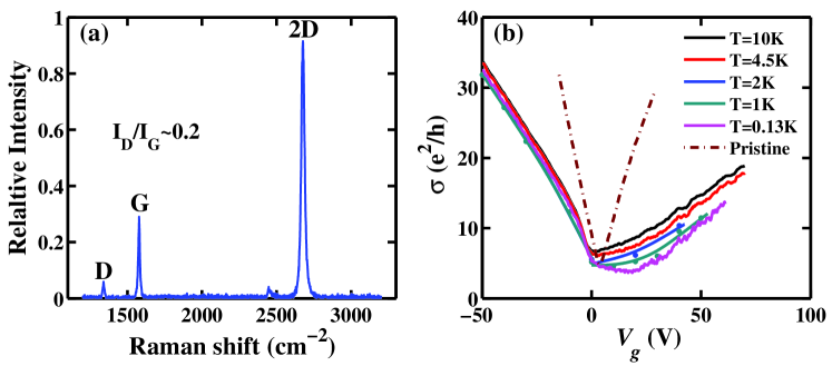
We now turn to the gate voltage dependence of conductivity of defected graphene. For typical pristine graphene, the dependence displays a slight asymmetry with respect to the Dirac point, which is usually ascribed to the difference between scattering off an attractive potential and off a repulsive one Novikov (2007). However, in defected graphene, a strong asymmetry appears [see Fig. 1(b)]. The slope on the hole side (negative gate voltage) is substantially larger than that on the electron side (positive gate voltage). The field effect mobilities for hole and electron are 1650 cm2/Vs () and 738 cm2/Vs (), respectively. The resultant ratio is , appreciably smaller than that of typical pristine graphene and potassium doped graphene Chen et al. (2008). Furthermore, the evolution of the conductance is different for holes and electrons. With increase of the hole density, a steep increase of the conductivity with the gate voltage in the vicinity of the Dirac point is followed by a weaker linear dependence at high carrier density. On the contrary, for electrons, the conductivity undergoes a slow increase and then develops a larger slope. The most striking feature is that the temperature dependence of the conductivity displays distinctive behavior for holes and electrons, i.e., virtually independent of for holes, while strongly dependent for electrons. These unusual behaviors suggest that scattering mechanism is fundamentally different in the two regions.
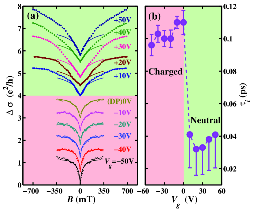
Magnetoconductivity data support different scattering mechanisms in the two regions. The change of the conductivity with the magnetic field, , is depicted in Fig. 2(a). In the hole region, a narrow dip appears around . However, in the electron region, it becomes much broader. The dip structure originates from weak localization. It is a direct consequence of intervalley scattering McCann et al. (2006). It is well known that the interference of electron waves along time-reversal paths gives rise to a quantum correction to the conductivity. A magnetic field suppresses the correction by randomizing the phases of interfering waves. In intrinsic graphene, the inference is destructive because of a Berry phase of . As a result, the magnetoconductivity is negative, i.e., weak antilocalization(WAL). In the presence of intervalley scattering, the magnetoconductivity in low fields turns positive, i.e.,weak localization (WL). The width of the WL dip is directly related to the strength of intervalley scattering. Roughly, the width is inversely proportional to the intervalley scattering time , . Here, is the elementary charge, the reduced Planck constant, and the diffusion constant. So, the data in Fig. 2(a) clearly show that intervalley scattering rate is much larger on the electron side than on the hole side.
Quantitative estimation of can be obtained by fitting the experimental data to an equation widely used to describe WAL in graphene McCann et al. (2006):
| (2) |
where is the digamma function, the phase coherence time, and the intravalley scattering time. The fitted parameter as a function of is plotted in Fig. 2(b). On the hole side, is about 0.1 ps. After the Fermi level passes the Dirac point towards the electron side, it suddenly drops to 0.04 ps, which is the lower bound set for fitting. In the theory of WL, electrons are assumed to be diffusive, i.e. . Here, is the mean-free time, which can be calculated from the conductivity. To satisfy the assumption, was set as the lower bound of the fitting parameter . The fact that reached the bound indicates dominance of intervalley scattering by defects, which is consistent with the average distance of 23 nm between defects inferred from the Raman spectrum. The deviation of data from fitting curves is most likely due to the assumption of Eq. (2) being no longer held, which implies that the actual is less than . Nevertheless, it is unambiguous that the intervalley scattering rate is strongly suppressed on the hole side.
Intervalley scattering is caused by atomically sharp short-range potentials, such as defects. However, the defect concentration will apparently not change with . The only plausible explanation is that a mechanism prevents carriers from “seeing” defects. The electronic structure of defects in graphene has been theoretically studied Pereira et al. (2006); Wehling et al. (2007); Nanda et al. (2012). There is a general consensus that defects introduce resonant states at the Dirac point Not . The resonance state has been confirmed experimentally Ugeda et al. (2010). When the Fermi level passes the Dirac point, the resonant states will be populated/unpopulated, which corresponds to neutral/charged states of defects. This gate-controlled charging effect for defects has been demonstrated in a scanning tunneling microscopy study Brar et al. (2011), in which not only a defect resonance state has been observed, but ionization of a defect by tip induced gating has been realized. A recent experimental study, combined with theoretical calculations, has also shown that defects are positively charged Liu et al. (2014). Therefore, on the hole side, where defects are ionized (charged), the long-range Coulomb potential can deflect carriers and reduce the scattering cross section of the short-range potential, leading to suppression of intervalley scattering.
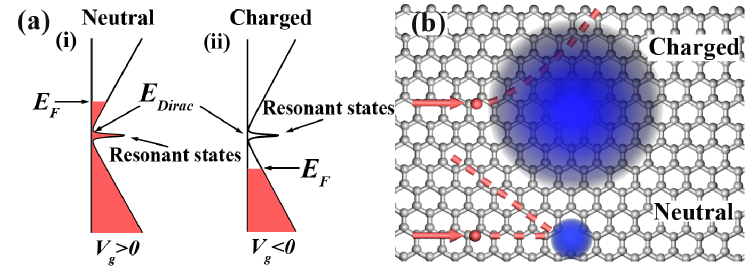
The proposed mechanism is illustrated in Fig. 3. Impurity resonant states form at the Dirac point. When the Fermi level is above the Dirac point, impurity states are filled and defects are neutral. Carriers can approach defects and be scattered by short-range potential. Significant intervalley scattering leads to strong weak localization, which is temperature dependent. In contrast, when the Fermi level is below the Dirac point, impurity states are empty and defects are charged. Long-range Coulomb potentials dominate carrier scattering. Few carriers can penetrate the Coulomb potential and be scattered by the short-range potential, resulting in suppression of intervalley scattering. Since the short-range potential contributes more to momentum relaxation than the long-range one in graphene, the mobility exhibits substantial asymmetry.
Around the Dirac point, when the gate voltage is swept from positive to negative, defects go through a transition from a neutral to a charged state. The scattering cross section of the short-range potential continuously decreases because it is screened by the long-range Coulomb potential of charged defects. The total scattering cross section is also reduced as the short-range potential is more effective in scattering carriers than the long-range one, indicated by the asymmetry of the conductivity. On the other hand, the carrier density decreases first and then increases after passing the Dirac point. The combination of the two effects leads to a weak gate dependence of conductivity on the right side of the Dirac point, while to a strong increase of conductivity on the left side, which is in excellent agreement with the experimentally observed evolution of the conductivity near the Dirac point.
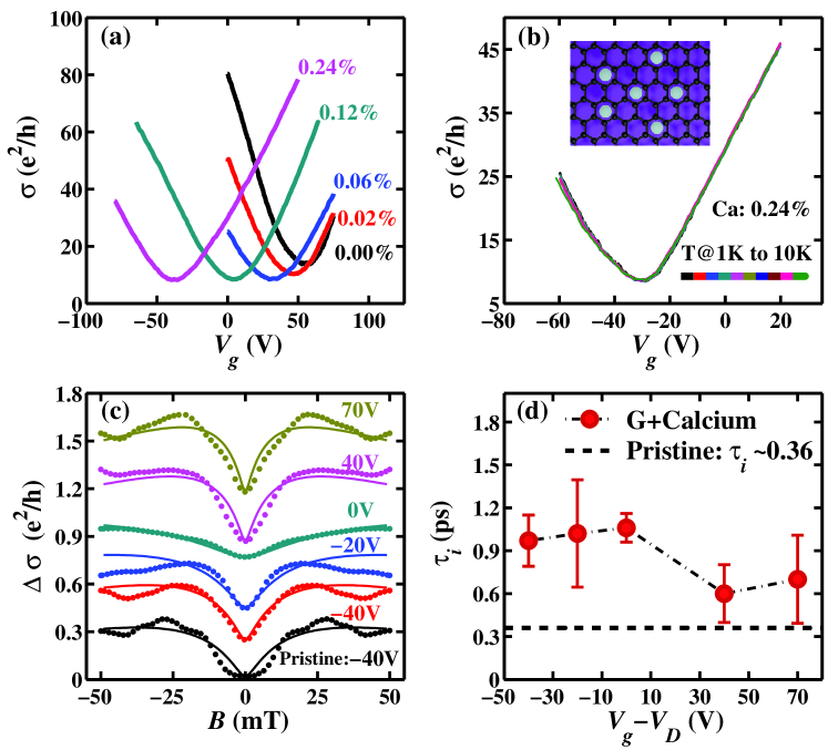
To further confirm the suppression of intervalley scattering by Coulomb potential, transport experiments were performed on calcium-doped graphene. According to previous theoretical calculations, Ca adatoms form ionic bonds to graphene and are only Å away from the graphene sheet Chan et al. (2008). The charge transfer per Ca adatom is predicted to be 0.78Chan et al. (2008). So, the potential should have both a short-range part and a long-range part, just like a charged defect. This should hold even if the actual bond length may deviate from the 2.3 Å, as it only yields variation of the strength of the short-range part. The transport data are shown in Fig. 4. Upon Ca deposition, the Dirac point shifts towards the negative gate voltage, suggesting electron doping. Note that Ca adatoms stay in a positively charged state in the whole range of gate voltage. No apparent temperature dependence was observed, consistent with defected graphene when defects are charged. Mobility decreases due to additional scattering by adatoms. Interestingly, the weak-localization peak in the magnetoconductivity became slightly narrower after Ca deposition. Note that the peak should be wider when the mobility is reduced, even if the intervalley scattering is not changed. So, not only did Ca adatoms not introduce intervalley scattering, but the intervalley scattering was suppressed. By fitting data to Eq. (2), we obtained the intervalley scattering time, which indeed increased from 0.36 to about 0.8 ps. Thus, absence of enhancement of intervalley scattering in Ca-doped graphene corroborates with suppressed intervalley scattering in defected graphene when defects are charged.
In conclusion, our experiment unambiguously shows that the long-range part of a potential can strongly reduce the transport cross section of the short-range part. In a multivalley system, this means suppression of intervalley scattering. Therefore, this effect is particularly relevant in materials promising for valleytronics, such as graphene and TMDs. Furthermore, we would like to point out that it also provides important insight into another topic in which adatoms have been proposed to engineer the properties of graphene, such as spin-orbit coupling Castro Neto and Guinea (2009); Weeks et al. (2011); Jiang et al. (2012); Ferreira et al. (2014); Cresti et al. (2014) and magnetism Sevincli et al. (2008); Qiao et al. (2010); Cao et al. (2010); Virgus et al. (2014). Despite many theoretical proposals, transport studies have shown that Au, Mg and In adatoms on graphene generate only long-range Coulomb impurity scattering, while neither spin-orbit scattering nor magnetic scattering has been introduced Pi et al. (2010); Swartz et al. (2013); Jia et al. (2015); Chandni et al. (2015). Since all these adatoms are charged, our result points to a reasonable explanation and a hint for possible solutions.
Acknowledgements.
This work was supported by the National Key Basic Research Program of China (No. 2012CB933404 and No. 2013CBA01603) and NSFC (Projects No. 11074007, No. 11222436, and No. 11234001).References
- Rycerz et al. (2007) A. Rycerz, J. Tworzydlo, and C. W. J. Beenakker, Nature Phys. 3, 172 (2007).
- Xu et al. (2014) X. Xu, W. Yao, D. Xiao, and T. F. Heinz, Nat Phys 10, 343 (2014).
- Xiao et al. (2007) D. Xiao, W. Yao, and Q. Niu, Phys. Rev. Lett. 99, 236809 (2007).
- Mak et al. (2012) K. F. Mak, K. He, J. Shan, and T. F. Heinz, Nat. Nanotechnol. 7, 494 (2012).
- Zeng et al. (2012) H. Zeng, J. Dai, W. Yao, D. Xiao, and X. Cui, Nat. Nanotechnol. 7, 490 (2012).
- Gorbachev et al. (2014) R. V. Gorbachev, J. C. W. Song, G. L. Yu, A. V. Kretinin, F. Withers, Y. Cao, A. Mishchenko, I. V. Grigorieva, K. S. Novoselov, L. S. Levitov, et al., Science 346, 448 (2014).
- Ju et al. (2015) L. Ju, Z. Shi, N. Nair, Y. Lv, C. Jin, J. Velasco, C. Ojeda-Aristizabal, H. A. Bechtel, M. C. Martin, A. Zettl, et al., Nature 520, 650 (2015).
- Sui et al. (2015) M. Sui, G. Chen, L. Ma, W. Shan, D. Tian, K. Watanabe, T. Taniguchi, X. Jin, W. Yao, D. Xiao, et al., et al., Nat Phys 11, 1027 (2015).
- Wu et al. (2013) S. Wu, C. Huang, G. Aivazian, J. S. Ross, D. H. Cobden, and X. Xu, ACS Nano 7, 2768 (2013).
- Nomura and MacDonald (2007) K. Nomura and A. H. MacDonald, Phys. Rev. Lett. 98, 076602 (2007).
- Adam et al. (2007) S. Adam, E. H. Hwang, V. M. Galitski, and S. Das Sarma, Proc. Natl. Acad. Sci. 104, 18392 (2007).
- Hwang et al. (2007) E. H. Hwang, S. Adam, and S. Das Sarma, Phys. Rev. Lett. 98, 186806 (2007).
- Chen et al. (2009) J.-H. Chen, W. G. Cullen, C. Jang, M. S. Fuhrer, and E. D. Williams, Phys. Rev. Lett. 102, 236805 (2009).
- Wehling et al. (2010) T. O. Wehling, S. Yuan, A. I. Lichtenstein, A. K. Geim, and M. I. Katsnelson, Phys. Rev. Lett. 105, 056802 (2010).
- Peres (2010) N. M. R. Peres, Rev. Mod. Phys. 82, 2673 (2010).
- McCann et al. (2006) E. McCann, K. Kechedzhi, V. I. Fal’ko, H. Suzuura, T. Ando, and B. L. Altshuler, Phys. Rev. Lett. 97, 146805 (2006).
- Wu et al. (2007) X. S. Wu, X. Li, Z. Song, C. Berger, and W. A. de Heer, Phys. Rev. Lett. 98, 136801 (2007).
- Tikhonenko et al. (2008) F. V. Tikhonenko, D. W. Horsell, R. V. Gorbachev, and A. K. Savchenko, Phys. Rev. Lett. 100, 056802 (2008).
- Pereira et al. (2006) V. M. Pereira, F. Guinea, J. M. B. Lopes dos Santos, N. M. R. Peres, and A. H. Castro Neto, Phys. Rev. Lett. 96, 036801 (2006).
- Wehling et al. (2007) T. O. Wehling, A. V. Balatsky, M. I. Katsnelson, A. I. Lichtenstein, K. Scharnberg, and R. Wiesendanger, Phys. Rev. B 75, 125425 (2007).
- Brar et al. (2011) V. W. Brar, R. Decker, H.-M. Solowan, Y. Wang, L. Maserati, K. T. Chan, H. Lee, C. O. Girit, A. Zettl, S. G. Louie, et al., Nat. Phys. 7, 43 (2011).
- Chen et al. (2013) J. Chen, T. Shi, T. Cai, T. Xu, L. Sun, X. S. Wu, and D. Yu, Appl. Phys. Lett. 102, 103107 (2013).
- Nakada and Ishii (2011) K. Nakada and A. Ishii, Solid State Commun. 151, 13 (2011).
- Lucchese et al. (2010) M. Lucchese, F. Stavale, E. M. Ferreira, C. Vilani, M. Moutinho, R. B. Capaz, C. Achete, and A. Jorio, Carbon 48, 1592 (2010).
- Novikov (2007) D. S. Novikov, Appl. Phys. Lett. 91, 102102 (2007).
- Chen et al. (2008) J.-H. Chen, C. Jang, S. Adam, M. Fuhrer, E. Williams, and M. Ishigami, Nat. Phys. 4, 377 (2008).
- Nanda et al. (2012) B. R. K. Nanda, M. Sherafati, Z. S. Popovic, and S. Satpathy, New J. Phys. 14, 083004 (2012).
- (28) Although defects also introduce derived states according to Ref. Nanda et al., 2012, these states are far away from the Dirac point and half-filled (with three electrons). Thus, they do not contribute to the net charge of a vacancy.
- Ugeda et al. (2010) M. M. Ugeda, I. Brihuega, F. Guinea, and J. M. Gómez-Rodríguez, Phys. Rev. Lett. 104, 096804 (2010).
- Liu et al. (2014) Y. Liu, M. Weinert, and L. Li, Nanotechnology 26, 035702 (2014).
- Chan et al. (2008) K. T. Chan, J. B. Neaton, and M. L. Cohen, Phys. Rev. B 77, 235430 (2008).
- Castro Neto and Guinea (2009) A. H. Castro Neto and F. Guinea, Phys. Rev. Lett. 103, 026804 (2009).
- Weeks et al. (2011) C. Weeks, J. Hu, J. Alicea, M. Franz, and R. Wu, Phys. Rev. X 1, 021001 (2011).
- Jiang et al. (2012) H. Jiang, Z. Qiao, H. Liu, J. Shi, and Q. Niu, Phys. Rev. Lett. 109, 116803 (2012).
- Ferreira et al. (2014) A. Ferreira, T. G. Rappoport, M. A. Cazalilla, and A. H. Castro Neto, Phys. Rev. Lett. 112, 066601 (2014).
- Cresti et al. (2014) A. Cresti, D. Van Tuan, D. Soriano, A. W. Cummings, and S. Roche, Phys. Rev. Lett. 113, 246603 (2014).
- Sevincli et al. (2008) H. Sevincli, M. Topsakal, E. Durgun, and S. Ciraci, Phys. Rev. B 77, 195434 (2008).
- Qiao et al. (2010) Z. H. Qiao, S. Y. A. Yang, W. X. Feng, W. K. Tse, J. Ding, Y. G. Yao, J. Wang, and Q. Niu, Phys. Rev. B 82, 161414 (2010).
- Cao et al. (2010) C. Cao, M. Wu, J. Jiang, and H.-P. Cheng, Phys. Rev. B 81, 205424 (2010).
- Virgus et al. (2014) Y. Virgus, W. Purwanto, H. Krakauer, and S. Zhang, Phys. Rev. Lett. 113, 175502 (2014).
- Pi et al. (2010) K. Pi, W. Han, K. M. McCreary, A. G. Swartz, Y. Li, and R. K. Kawakami, Phys. Rev. Lett. 104, 187201 (2010).
- Swartz et al. (2013) A. G. Swartz, J.-R. Chen, K. M. McCreary, P. M. Odenthal, W. Han, and R. K. Kawakami, Phys. Rev. B 87, 075455 (2013).
- Jia et al. (2015) Z. Jia, B. Yan, J. Niu, Q. Han, R. Zhu, D. Yu, and X. Wu, Phys. Rev. B 91, 085411 (2015).
- Chandni et al. (2015) U. Chandni, E. A. Henriksen, and J. P. Eisenstein, Phys. Rev. B 91, 245402 (2015).