High-pressure melt growth and transport properties of SiP, SiAs, GeP, and GeAs 2D layered semiconductors
Abstract
Silicon and Germanium monopnictides SiP, SiAs, GeP and GeAs form a family of 2D layered semiconductors. We have succeeded in growing bulk single crystals of these compounds by melt-growth under high pressure (0.5-1 GPa) in a cubic anvil hot press. Large (mm-size), shiny, micaceous crystals of GeP, GeAs and SiAs were obtained, and could be exfoliated into 2D flakes. Small and brittle crystals of SiP were yielded by this method. High-pressure sintered polycrystalline SiP and GeAs have also been successfully used as a precursor in the Chemical Vapor Transport growth of these crystals in the presence of I2 as a transport agent. All compounds are found to crystallize in the expected layered structure and do not undergo any structural transition at low temperature, as shown by Raman spectroscopy down to T=5 K. All materials exhibit a semiconducting behavior. The electrical resistivity of GeP, GeAs and SiAs is found to depend on temperature following a 2D-Variable Range Hopping conduction mechanism. The availability of bulk crystals of these compounds opens new perspectives in the field of 2D semiconducting materials for device applications.
keywords:
A2. High-pressure melt growth , B2. Semiconducting materials , A1. Low dimensional structures , A2. Growth from vapor1 Introduction
2D materials are of great interest for the novel electronic properties that can arise from the reduced dimensionality and the quantum confinement of charge carriers, and have become more and more appealing for applications in modern electronic devices. After the epoch-making discovery of graphene [1], the search for stable free-standing atomic layers of semiconducting materials has experienced a rush and a fast improvement of the processing techniques. The wide family of transition metal dichalcogenides (TMDs) has proven to be the most promising, offering quite a large variety of compounds, large tunability of properties and flexibility in potential practical applications [2]. Electronic and optoelectronic devices based on various TMDs have been demonstrated [3, 4, 5]. The search for other families of 2D materials exhibiting the same properties, existing in stable atomic layers and offering similar potential for applications together with a natural abundance and a low production cost is still very active and deserves a strong effort. Chemically stable atomic layers with no surface dangling bonds can be obtained from other layered materials and the van der Waals-like bond between layers with different chemical compositions opens new perspectives for new heterostructures to be realized in a wide range of materials. Besides graphene, examples of pure elements from group IV (Si and Ge) and group V (P) have been found to form atomically thin layers (silicene [6], germanene [7] and phosphorene [8], respectively) that can be obtained through either chemical deposition on substrate [9] or mechanical exfoliation of bulk 3D crystals [10]. Binary compounds of a group IV element (Si, Ge, Sn) and a group V pnictogens (P, As, ) are also known to form layered structures in which 2D strongly covalent layers are stacked onto each other through weak van der Waals like bonds, as well as in TMDs. Silicon and germanium phosphides and arsenides have been reported since decades to crystallize in various layered structures with either orthorhombic (Cmc21 space group, SiP [11], Pbam space group, SiP2 and GeAs2 [12]) or monoclinic (C2/m space group, GeP, GeAs and SiAs [12, 13, 14]) symmetries. After the initial investigations of their crystal structures and phase equilibria, during the sixties and seventies, this family of compounds has been rather overlooked, and attracts today our interest as being a potential class of 2D materials, alternative to TMDs. The equilibrium phase diagrams assessed so far predict the existence of a limited number of stable compositions and polytypes [15]. Few more have been synthesised at high pressure (cubic GeP, cubic GeP2, rhombohedral GeP3 [16, 17]) or suggested to exist according to structural investigations, even though not present in the equilibrium phase diagram (orthorhombic SiP2[12] and cubic SiP2 [18]). Recently, the phase diagram of the Si-P has been theoretically revisited under high pressure and suggested to be substantially different from that drawn under equilibrium conditions at ambient pressure [19]. First principle calculations of phase stability in the Si-P system have predicted the existence of at least three new stable SixPy compounds with a layered structure that could be stable in single atomic layer forms [20]. Bulk crystals of these materials have been seldom if ever grown: SiAs was reported to crystallize from the melt by Sudo [21] and from the vapor phase by Kutzner et al. [22]; SiP and SiAs crystals were grown by the physical vapor transport (PVT) method [23], but resulted not to crystallize in the expected space group; very recently GeP was reported to grow in crystalline form by using a solution growth method in a flux of Bi and Sn [24]. As a matter of fact, the volatility and the strong reactivity and toxicity of pnictogens require the use of close reactors in order to prevent the vapor phase from escaping. Here we report about crystal growth of the four members of the family, namely SiP, SiAs, GeP and GeAs, from the self-flux under high pressure, using a cubic anvil hot pressure apparatus. Large, micaceous, and easy-to-cleave crystals were obtained in the case of GeP, GeAs, and SiAs. Small and brittle crystals were obtained in the case of SiP. Polycrystalline binary samples, processed in the same high-pressure furnace, were used as a precursor material for CVT growth experiments with iodine as a transport agent. This method was found to favor the growth of SiP and GeAs. This article reports on materials processing, crystal growth, structural and physical characterization of SiP, SiAs, GeP and GeAs. The crystals have the expected layered structure and can be exfoliated. These materials exhibit semiconducting behavior and confirm to have high potential as 2D materials for novel nano-engineered semiconducting devices.
2 Experimental
2.1 Thermodynamic considerations
The phase diagrams of the four systems under investigation have been assessed and are reported in the Pauling Files database [15]. Only two stable compounds are reported to exist in the Si-P and Ge-P diagrams, SiP and GeP, whose decomposition occurs at 1160∘C and 750∘C, respectively, via peritectic decomposition into elements P and Si, or Ge. According to those diagrams, SiP is reported to transform into a mixed solid-liquid-vapor phase [25], whereas GeP is claimed to decompose into solid Ge and liquid P [26]. At ambient pressure this appears quite unlikely, the sublimation temperature of P being as low as 430∘C. The Si-P phase diagram has been recently refuted and corrected by Liang et al. [19]. On the other hand, no recent thermodynamical investigations of the Ge-P system, or diagram updates, have been undertaken. Undoubtedly, the decomposition into a vapor phase of phosphorous at ambient pressure prevents from processing SiP and GeP by conventional techniques.
The phase diagrams of the systems containing As have been investigated by various authors (see [15] for a complete collection), and all agree on a congruent melting of SiAs and GeAs into a liquid phase at ambient pressure. This allows processing the compounds and growing the crystals under more conventional conditions. As a matter of fact, arsenic melts into liquid at ambient pressure and its vapor pressure is more than two orders of magnitude lower than that of P at the same temperature. In the case of SiAs and GeAs, the growth from the melt can be made more difficult by the presence of monoarsenide and diarsenide phases, both congruently melting in the same temperature range, which can grow into one another in the case of composition fluctuations and element segregation. Crystals of SiAs have been grown successfully from the melt under ambient pressure [23], as well as from the vapor phase under vacuum [22]. Only m-size crystals of GeAs have been obtained so far [13].
As a result of the above considerations, we have chosen a melt-growth method under high-pressure (in the GPa range) for all compounds. The calculated phase diagram of Si-P at 0.1 GPa [19], showing a solid-liquid equilibrium at the SiP composition, supports this choice. Moreover, high pressure has also been successfully used for growing crystals of black phosphorous preventing both its sublimation and the transformation into dangerous white phosphorous [27]. The use of pressures as high as 0.5-1 GPa is expected to make the growth of SiP and GeP from the melt possible. In the presence of As, the high pressure impedes the toxic vapor of As from reacting with the atmosphere, and speeds up the growth kinetics.
2.2 High-pressure melt growth (HP)
All crystals were grown in a high pressure cubic anvil press. Pure elements Si (6N), Ge (5N), P (5N) and As (5N) were used as reactants. They were mixed in a stoichiometric ratio and pressed into pellets of approximately 7 mm of diameter and 3 mm of thickness under uniaxial stress (3 tons). The pellets were then placed in a cylindrical boron nitride crucible surrounded by a graphite sleeve resistance heater and inserted into a pyrophyllite cube as a pressure transmitting medium. The pyrophyllite cell was then placed inside the high-pressure set-up, which consists of six WC anvils. For each composition, the cell was cold pressurized, then fast brought to high temperature (T1) at 1200∘C/hours, held for 30 min at this temperature and then slowly cooled to a temperature T2 before being quenched to room temperature, while maintaining a constant pressure (see Table 1 for details). The temperature T1 was chosen to be above the complete melting of the precursors. The quench temperature was chosen to be above any possible decomposition or phase transition. The slow cooling rate allows crystals to nucleate and grow.
| Sample | Pressure | T1(∘C) | T2(∘C) | Cooling (∘C/h) |
|---|---|---|---|---|
| SiP | 0.5/1 GPa | 1050 | 925 | 25 |
| SiAs | 1 GPa | 1200 | 1000 | 50 |
| GeP | 1 GPa | 900 | 600 | 100 |
| GeAs | 1 GPa | 900 | 650 | 50 |
2.3 Chemical Vapor Transport (CVT)
As mentioned above, vapor transport techniques are the most common way to obtain single crystals of these materials. However, owing to the large difference between the vapor pressure of the pnictogen and the group-IV element, very large temperature gradients (25∘C/cm) [28] were employed to achieve the right stoichiometry. In order to reduce such a strong technical constraint, we tried to grow crystals by vapor transport using smaller temperature gradients (5-7∘C/cm).
For the Physical Vapor Transport (PVT), the pure elements were mixed in a stoichiometric ratio, with a total mass of 0.2-0.3 g. The mixture was then placed in a quartz ampoule with an internal diameter of 8 mm and a length of 120 mm and sealed under vacuum (5x10⁻⁶ mbar). For the Chemical Vapor Transport (CVT), a transport agent (I2) was added to the pure elements according to a molar ratio n(I2)/n(Group IV) = 0.05. In both cases, the sealed reactor was placed in a two-zone furnace in the presence of a thermal gradient dT/dx 5-7∘C/cm, and heated up to Thot at the hot end, equal to 1100∘C and 900∘C for SiP and GeAs, respectively. After few days, the furnace was switched off and the temperature decreased to room temperature. Preliminary results confirmed the difficulties in maintaining the wanted stoichiometry during crystallization in both techniques, more dramatically in the PVT case, due to the rapid sublimation of the pnictogen element during heating. The addition of the transport agent proved to be insufficient to successfully control the growth process. According to these observations, we decided to start from different reactants and grow single crystal only by the CVT technique. Instead of using a mixture of pure elements, we started from high-pressure pre-reacted binary precursors mixed with the transport agent. This processing route proved to be successful to grow single crystals of SiP and GeAs.
2.4 Structural and Physical characterization
As-grown crystals were characterized by X-Ray diffraction (XRD), SEM-EDX analysis, Raman Spectroscopy, and electrical transport. XRD patterns were acquired in a Philips X’Pert four-circle diffractometer and a Philips PW1820 powder diffractometer, both using Cu K radiation. Thanks to their better quality, only GeP and GeAs crystals could also be measured in an Agilent Super Nova single crystal diffractometer using MoK radiation. SEM-EDX analysis were carried out in a LEO 438VTP electron microscope coupled to a Noran Pioneer X-Ray detector. Raman spectroscopy was performed with a homemade micro Raman spectrometer equipped with an argon laser ( = 514.5 nm, spectral resolution of 1 cm-1) and a helium-flow cryostat working from 300K to 4 K. The electrical resistivity was measured by the standard four-probe method using a Quantum Design PPMS (physical properties measurement system) from 300 K to 2 K under a magnetic field from 0 to 7 T.
3 Results and Discussion
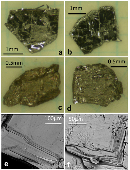
Pictures of single crystals of SiP, SiAs, GeP and GeAs grown by the HP method are presented in Fig. 1. As shown in these pictures, it is easier to grow the pnictides of germanium than those of silicon. Single crystals of GeP, GeAs and in a lesser measure SiAs are large, shiny and present grey flakes that can be easily cleaved into thinner flakes. On the other hand, SiP crystals are significantly smaller, less shiny, and very brittle. The peculiar lower quality of SiP crystals is ascribable to various facts: SiP is the only monopnictide that crystallizes in the orthorhombic space group Cmc21 instead of the monoclinic C2/m, which is common to the other compositions. Moreover, according to the phase diagram reported by Liang et al. [19], the temperature range suitable for nucleation and growth of SiP is rather narrow. Besides, the isostatic pressure can only be increased over a little range for avoiding the formation of other HP metastable SixPy phases [29]. Congruent melt conditions were achieved for all systems: SEM-EDX analysis confirms the expected 1:1 chemical composition of the crystals and neither composition fluctuations nor secondary phases have been noticed in the core of the HP-grown bulk. SEM images, figure 1(e-f), evidence the lamellar structure of these crystals and their suitability for fabricating 2D devices. The same analysis on the GeAs and SiP crystals grown by the CVT method also confirms the 1:1 stoichiometry, with no traces of the transport agent I2.
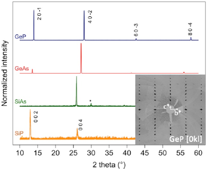
Crystals cleave easily in the plane corresponding to the van der Waals gap (see Fig. 2) and clean powder diffraction patterns, with a strong preferred orientation, were obtained. This is confirmed by the -2 scans shown in Fig. 3, which are compatible with a monoclinic symmetry C2/m with strong preferred orientation along the [2 0 -1] direction. For GeP and GeAs, good quality single crystals could be cleaved to confirm the crystal structure (the reciprocal space reconstruction for the plane [0 k l] for GeP is shown as an inset in Fig. 3). The powder diffraction pattern for SiP presents broader reflections but agrees with the orthorhombic space group Cmc21 with preferred orientation along the [0 0 1] direction.
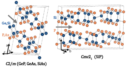
The diffraction patterns obtained from the cleavage planes of the two different structures in the same Bragg-Brentano geometry are very similar. This is accounted for by the similar local symmetry in the planes and the (Si,Ge)-(P,As) polyhedra that order in similar chains in these planes, as described in ref. [11].
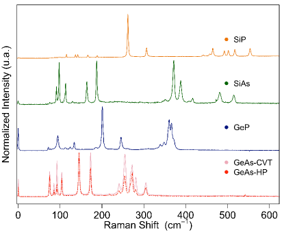
All samples were also characterized by Raman spectroscopy. The narrow, well defined peaks of the Raman shift, as well as the very low level of background proved the general good quality of the crystals. Fig. 4 shows the Raman spectra of SiP, SiAs, GeP and GeAs (from top to bottom, respectively). The Raman shift in SiAs is in good agreement with the previous Raman study reported by Kutzner et al.[22]. The three compounds with a monoclinic structure exhibit similar Raman spectra (similar groups of modes, red-shifting when going from lighter to heavier compounds). Unequivocally, the Raman shift of SiP is different from the others, confirming the different crystal structure of SiP. The bottom-most plot shows two patterns of GeAs crystals grown by different techniques (HP and CVT): the reproducibility of the Raman spectrum confirms the quality of the samples and the reliability of the processing routes. Indexation of the Raman modes of GeAs, GeP and SiP is not known at this stage. DFT calculations of the phonon spectra are in progress. The Raman study as a function of temperature shows no significant changes down to 5 K, indicating that no structural transitions occur and the symmetry is preserved.
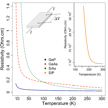
Electrical resistivity measurements were performed on several HP-grown single crystals of each composition from room temperature to 5K. Small deviations in the resistivity from one sample to another with the same composition are consistent with the difficulty in correctly estimating the thickness of these small, layered crystals. As pointed out in Fig. 5 , the four pnictides exhibit semiconducting behavior. The values of electrical resistivity at room temperature are in the same range for the monoclinic compounds, GeP (0.02 cm), SiAs (0.038 cm), GeAs (0.071 cm). On the other hand, for the orthorhombic SiP the electrical resistivity is four order of magnitude larger (141 cm), as shown in the inset of Fig. 5 ; the high resistance of SiP prevents the complete characterization over the whole temperature range. The large electrical resistivity of SiP, as compared to the other members of the family, was reproducible over samples from various batches and is likely to be related to the structural difference between SiP and the other monopnictides. No magnetoresistance effect is observed by repeating the (T) measurements under magnetic fields up to 7 tesla.
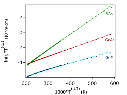
Despite their evident semiconducting behavior, a simple thermally activated Arrhenius law does not fit to the experimental resistivity of the monoclinic compounds. As a matter of fact the dependence of the resistivity on temperature is very well described by a Variable-Range-Hopping model [30]. According to this model, the resistivity obeys the law
| (1) |
where T0 is a constant and depends on temperature as the square root of T [31]. The factor n in the exponent indicates the dimensionality of the system, so that the exponent 1/(n+1)=1/3 in a two-dimensional system. The plot of ln(T-1/2) versus T(-1/3) shown in Fig.5 for the three compounds GeP, GeAs and SiAs, evidences a linear trend between T=5 K and T=120 K and agrees with a Variable-Range-Hopping conduction in a 2-dimensional system. This is consistent with the 2D-like structure of these materials and confirms that the electrical conduction involves only the (Ge,Si)-pnictide bonds in the quasi-2D slab oriented in the [2l 0 -l] direction. This behavior is expected on the base of the calculation of the Electron Localization Function (ELF) in GeP reported by Lee et al. [24] that predicts the absence of covalent bonds between the layers and strong covalent Ge-Ge and Ge-P bonds in the layer.
The slope of the linear dependence of ln(T-1/2) on T-1/3 shown in Fig. 6 is higher in SiAs than in the two Ge-pnictides (for which it is the same). Such slope, that is T0 in equation (1), is proportional to the hopping distance and inversely proportional to the density of state at the Fermi level, N(EF) [31]. The higher T0 would indicate that in SiAs the density of growth-induced defects is lower. On the other hand, the equal slope observed in GeP and GeAs VRH-linear regression suggests that the origin of localized impurity states in the gap cannot be ascribed to occupation vacancies or substitutional defects on the pnictogen site, but are more likely related to the slightly disordered local coordination of Ge, predicted by ELF calculations [24].
4 Conclusions
With the aim of searching for 2D layered semiconducting materials that can be exfoliated down to atomically thin layers, we have investigated the family of Si- and Ge-monopnictides (SiP, SiAs, GeP, GeAs). Bulk crystals of these compounds were rarely grown, had small size and never allowed systematic investigations of their electronic properties. The crystal structure in which these materials crystallized was object of controversy. In this work we have shown that high pressure (in the GPa range) favors the crystal growth of the four Si- and Ge-monopnictides. Those containing Ge, in particular, can be grown with a large size (up to 4-5 mm2 in the cleavage plane). Crystals of SiP and GeAs could also be grown by the vapor transport technique, provided that high-pressure pre-reacted elements were used as precursors and I2 was used as transport agent. We have confirmed the monoclinic space group C2/m for SiAs, GeP and GeAs, and the orthorhombic Cmc21 for SiP. All compounds exhibit a semiconducting behavior. Nevertheless, the electrical resistivity of three of them (SiAs, GeP and GeAs) is found to follow a 2D Variable Range Hopping conduction mechanism at low temperature. These materials can be mechanically exfoliated and the study of their properties as a function of the flake thickness is in progress.
5 Acknowledgements
The authors gratefully thank J. Teyssier for his precious help in Raman spectroscopy experiments. This work was partially supported by the Swiss National Science Foundation through the ”Sinergia” project n. CRSII2-147607.
6 References
References
- [1] K. S. Novoselov, A. K. Geim, S. V. Morozov, D. Jiang, Y. Zhang, S. V. Dubonos, I. V. Grigorieva, A. A. Firsov, Science 80 (2004) 666-669.
- [2] M. Chhowalla, H. S. Shin, G. Eda, L.-J. Li, K. P. Loh, H. Zhang, Nat. Chem. 5 (2013) 263-75.
- [3] B. Radisavljevic, A. Radenovic, J. Brivio, V. Giacometti, A. Kis, Nat. Nanotechnol. 6 (2011) 147-150.
- [4] H. Wang, L. Yu, Y.-H. Lee, Y. Shi, A. Hsu, M. L. Chin, L.-J. Li, M. Dubey, J. Kong, T. Palacios, Nano Lett. 12 (2012) 4674-4680.
- [5] M. Tosun, S. Chuang, H. Fang, A. B. Sachid, M. Hettick, Y. Lin, 8 (2014) 4948-4953.
- [6] P. Vogt, P. De Padova, C. Quaresima, J. Avila, E. Frantzeskakis, M. C. Asensio, A. Resta, B. Ealet, G. Le Lay, Phys. Rev. Lett. 108 (2012) 1-5.
- [7] M. E. Dávila, L. Xian, S. Cahangirov, A. Rubio, G. Le Lay, New J. Phys. 16 (2014) 095002.
- [8] L. Li, Y. Yu, G. J. Ye, Q. Ge, X. Ou, H. Wu, D. Feng, X. H. Chen, Y. Zhang, Nat. Nanotechnol. 9 (2014) 372-377.
- [9] B. Lalmi, H. Oughaddou, H. Enriquez, A. Kara, S. Vizzini, B. Ealet, Appl. Phys. Lett. 97 (2010) 223109.
- [10] A. Kara, H. Enriquez, A. P. Seitsonen, L. C. L. Y. Voon, S. Vizzini, B. Aufray, Surf. Sci. Rep. 67 (2012) 1-18.
- [11] T. Wadsten, Chem. Scripta 8 (1975) 63-69.
- [12] T. Wadsten, Acta Chem. Scand. 21 (1967) 593-594.
- [13] B. F. Mentzen, Comptes Rendus de l’Acad mie des Sciences Srie 2 293 (1981) 965.
- [14] T. Wadsten, S. Burmester, G. Cederberg, R. B. Jensen, C. T. Pederson, E. Larsen, Acta Chem. Scand. 19 (1965) 1232-1238.
- [15] P. Villars, Pauling Files Binaries Edition, Crystal Impact (2002).
- [16] J. Osugi, R. Namikawa, Y. Tanaka, Rev. Phys. Chem. Japan 37 (1967) 81-93.
- [17] J. Gullman, O. Olofsson, J. Solid State Chem. 5 (1972) 441-445.
- [18] T. Wadsten, Acta Chem. Scand. 21 (1967) 1374-1376.
- [19] S.-M. Liang, R. Schmid-Fetzer, J. Phase Equilibria Diffus. 35 (2014) 24-35.
- [20] B. Huang, H. L. Zhuang, M. Yoon, B. G. Sumpter, S.-H. Wei, Phys. Rev. B 91 (2015) 1-5.
- [21] I. Sudo, Jpn. J. Appl. Phys. 19 (1980) 755-756.
- [22] J. Kutzner, J. Kortus, O. P tzold, U. Wunderwald, G. Irmer, J. Raman Spectrosc. 42 (2011) 2132-2136.
- [23] C. G. Beck, R. Stickler, J. Appl. Phys. 37 (1966) 4683-4687.
- [24] K. Lee, S. Synnestvedt, M. Bellard, K. Kovnir, J. Solid State Chem. 224 (2015) 62-70.
- [25] B. Giessen, R. Vogel, Z. Met. 50 (1959) 274-277.
- [26] Y. A. Ugai, L. I. Sokolov, E. G. Goncharov, V. R. Pshenstanchik, Russ. J. Inorg. Chem. 23 (1978) 1048-1050.
- [27] S. Endo, Y. Akahama, S. Terada, S. Narita, Jpn. J. Appl. Phys. 21 (1982) L482-L484.
- [28] T. Wadsten, Acta Chem. Scand. 23 (1969) 331-333.
- [29] J. Osugi, R. Namikawa, Y. Tanaka, Rev. Phys. Chem. Jpn 36 (1966) 35-43.
- [30] N. F. Mott, J. Non Cryst. Solids 1 (1968)1-17.
- [31] N. V. Argiskaya, V. I. Kozub, J. Exp. Theor.Phys. 79 (1994) 466-472.