Direct observation of local Rashba spin polarization and spin-layer locking in centrosymmetric monolayer PtSe2
Abstract
The generally accepted view that spin polarization is induced by the asymmetry of the global crystal space group has limited the search for spintronics Spintronics materials to non-centrosymmetric materials. Recently it has been suggested that spin polarization originates fundamentally from local atomic site asymmetries ZungerNatPhys , and therefore centrosymmetric materials may exhibit previously overlooked spin polarizations. Here by using spin- and angle-resolved photoemission spectroscopy (spin-ARPES), we report helical spin texture induced by local Rashba effect (R-2) in centrosymmetric monolayer PtSe2 film. First-principles calculations and effective analytical model support the spin-layer locking picture: in contrast to the spin splitting in conventional Rashba effect (R-1), the opposite spin polarizations induced by R-2 are degenerate in energy while spatially separated in the top and bottom Se layers. These results not only enrich our understanding of spin polarization physics, but also may find applications in electrically tunable spintronics.
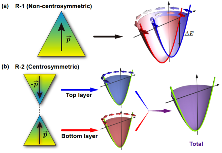
The new insight that spin polarization in nonmagnetic materials originates from relativistic spin-orbit coupling (SOC) from the local asymmetry (atomic site group) ZungerNatPhys ; SpinNewsViews ; KingNatPhys ; SpinNewsViews2 rather than the global asymmetry (bulk space group) has revolutionized our understanding of spin polarization physics. This has led to two forms of hidden spin polarization in centrosymmetric materials, R-2 (by site dipole field) and D-2 (by site inversion asymmetry) to be distinguished from the conventional Rashba (R-1, by dipole field) Rashba ; RashbaRev ; LaShellAu ; Bi111 ; Bi111K ; Ir111 ; IshizakaBiTeI ; BahramyPRB and Dresselhaus (D-1, by bulk inversion asymmetry) Dreselhauss effects previously discovered in non-centrosymmetric materials. Different from the R-1 effect with a net spin polarization, the R-2 effect is characterized by compensated spin polarizations of opposite signs that are spatially segregated into two real space sectors forming the inversion partners, e.g. top and bottom layers (see schematic cartoon in Fig. 1). Compared to the R-1 effect with a large internal electric field which is difficult to be reversed by an external field, the spins induced by R-2 might have advantages for electrically tunable spintronics devices due to the easy manipulation via the application of an external electric field LaOBiS2NL ; ZungerPRB . Layered transition metal dichalcogenides (TMDs) ZhangHNatureChem ; YaoWRev ; WangFpseudoBWSe2 ; XuXD are good candidates for realizing the R-2 effect due to the large SOC and large site dipole field. Although hidden spin polarization has been recently reported in the bulk crystal of WSe2 KingNatPhys and predicted in other layered materials, e.g. LaOBiS2 LaOBiS2NL ; ZungerPRB and (LaO)2(SbSe2)2LaOSbSe2 films, so far stable semiconducting thin films with large spin polarization induced by the R-2 effect still remain to be realized experimentally.
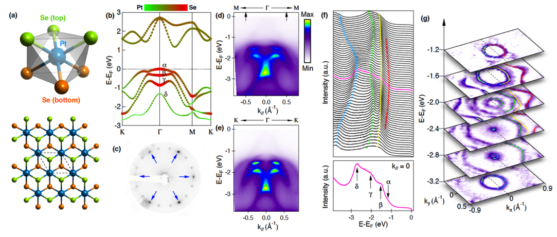
Monolayer PtSe2 contains one Pt layer sandwiched between two Se layers, forming trigonal structure when projected onto the (001) plane (Fig. 2(a)). It has centrosymmetric space group Pm1 for bulk structure, polar point group C3 for both Pt and Se sites, and it is semiconducting PtSe2NL . These properties make it a promising candidate for realizing electrically tunable spintronics by R-2 effect ZungerNatPhys . First-principles calculations (Fig. 2(b)) show that the top three valence bands (labeled by , and ) are mostly contributed by the p orbitals of Se, and the fourth valence band (labeled by ) is mainly contributed by the d orbitals of Pt. From the calculations, all the bands should be doubly degenerate without any net spin polarization since monolayer PtSe2 has both inversion and time-reversal symmetries. Here, by combining a full three-dimensional spin analysis using spin-ARPES and theoretical calculations, we report the hidden helical spin texture and spin-layer locking in monolayer PtSe2 induced by R-2 effect.
Figure 2(c) shows the low energy electron diffraction (LEED) pattern of the high quality monolayer PtSe2 thin film grown on Pt(111) substrate PtSe2NL . The semiconducting property of monolayer PtSe2 has been reported PtSe2NL . ARPES data measured along two high symmetry directions M--M (Fig. 2(d)) and K--K (Fig. 2(e)) show similar dispersions, suggesting that the electronic structure is overall rather isotropic. Correspondingly, circular shape is observed in the constant energy maps (Fig. 2(g)) for all the bands, and hexagonal warping is observed at relatively high binding energy. Analysis from energy distribution curves (EDCs) shows that the measured dispersions are in good agreement with first-principles calculations (Fig. 2(b)) and the four valence bands are separated from each other at the point.
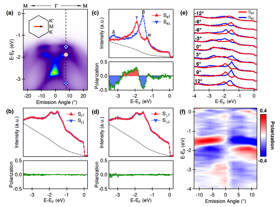
Figure 3 shows the three dimensional spin analysis for data measured along the M--M direction. A large spin contrast is observed along the tangential direction () for , and bands at emission angle of 7.5° (dashed line in Fig. 3(a)) with up to 50 polarization (Fig. 3(c)), while negligible spin contrast is observed along the radial (r) and out-of-plane () directions (Figs. 3(b,d)). The spin directions are illustrated by blue crosses (into the plane) and red dots (out of the plane) in Fig. 3(a). We extend the in-plane tangential spin analysis to other momenta along the M--M direction. Figure 3(e) shows the intensity distribution at different emission angles for spin-up and spin-down states along the tangential direction, and the spin polarization is shown in Fig. 3(f). When approaching the point from M point, the degree of spin polarization decreases and it becomes negligible at the point. On the other side of the point, the spin polarization is reversed. The observation of spin polarization along the in-plane tangential direction with opposite signs on the two sides of the point suggests that these bands may exhibit helical spin texture.
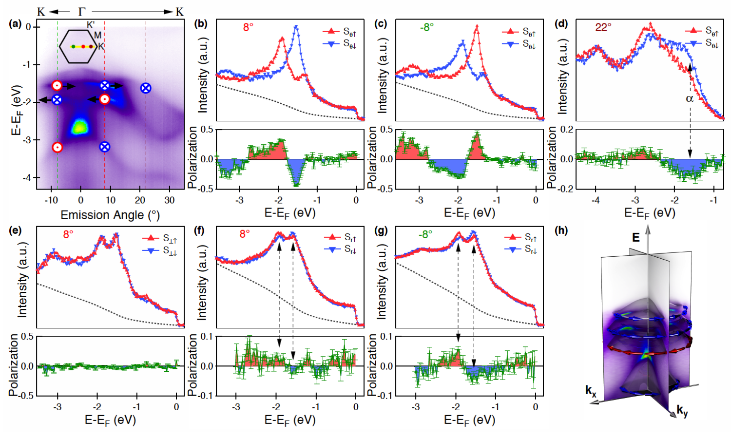
Figure 4 shows the spin analysis for data measured along the K--K direction. A large spin polarization is also observed for the tangential component (Figs. 4(b, c)), in agreement with helical spin texture. The band shows negligible spin polarization near the point. When moving to a large emission angle along the -K direction, the band is separated from other bands and we can resolve its spin polarization more easily here. In Fig. 4(d), spin polarization is observed in the band and its direction is determined to be the same as band. Considering that the electronic structure is rather isotropic, the observed large spin polarization for the tangential direction along both -K and -M directions suggests that the spin polarization has an overall helical texture. Different from the -M direction, a small yet detectable spin polarization of 5 is observed in the radial component for and bands with opposite spin directions (Figs. 4(f, g)), and its polarization does not reverse for opposite sides of the point. This suggests that the spin structures near the K and K′ points in Brillouin zone are not equivalent. This could be related to the defects in sample or other underlying mechanism such as final-state effect. Combining all spin-ARPES measurements discussed above, monolayer PtSe2 on Pt(111) shows overall helical spin textures with different helicities in the four bands as summarized in the schematic drawing in Fig. 4(h).
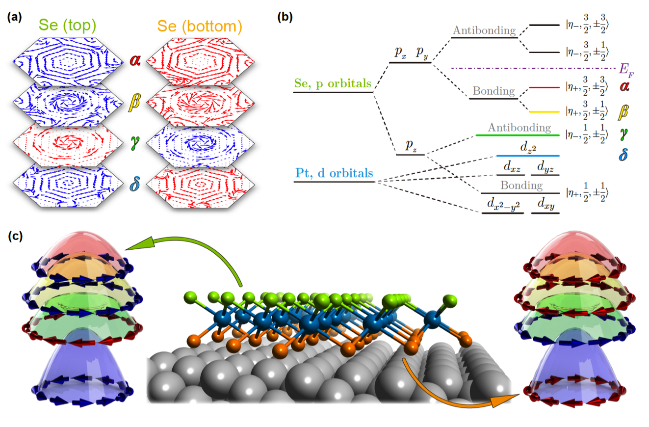
The observed helical spin texture is fundamentally different from that of the R-1 effect. For the conventional R-1 Rashba effect, two spin-splitting bands possess opposite spin helicities and their eigen-energies become degenerate at the point () due to TR symmetry, as shown in Fig. 1(a). In contrast, all these four bands are well split at the point, as clearly shown in Fig. 2(f). In additional, the and bands share the same spin helicities, completely different from the R-1 effect. Compared to the first-principles calculations in Fig. 2(b), it seems confusing that although energy dispersion agrees well between theory and experiments, spin texture does not appear in the calculations due to double degeneracy of two spin bands. This discrepancy can be understood by recognizing the fact that the light for ARPES measurements has a limited penetration depth and thus the top Se layer contributes more significantly to the observed spin polarization. To test this idea, we project spin polarization into the top and bottom Se layers and helical spin textures indeed emerge in each Se layer, as shown in Fig. 5(a). Strikingly, the obtained spin textures on the top Se layer in Fig. 5(a) reproduce qualitative features observed in spin-ARPES measurements for all four bands. For example, the and bands indeed have the same spin polarization while those of and bands are opposite. For the band, the spin polarization is negligible compared to that of the band close to the point. The consistency between the calculations and experiments suggests that layer-dependent spin texture (Fig. 5(c)), which was also theoretically proposed in other layered materials including LaOBiS2 LaOBiS2NL ; ZungerNatPhys and (LaO)2(SbSe2)2 LaOSbSe2 thin films, plays an essential role in understanding our spin-ARPES results. The existence of spin-layer locking can be understood as a natural consequence of the common sandwich type of crystal structures in all these materials, in which local electric fields are expected to point from the two outer Se layers to the central Pt layer.
More theoretical understanding can be obtained by analyzing the orbital natures of these four bands at the point (the atomic limit), as shown in Fig. 5(b). It is found that the orbitals of Se atoms dominates the bands near the Fermi energy and the orbitals of Pt atoms are fully occupied. The strong anisotropy introduce a strong energy splitting between the orbitals and the orbital of Se atoms, pushing Se orbitals to lower energy. As a result, the conduction and valence bands around the band gap mainly consist of the orbitals of Se atoms. The hybridization of the Se orbitals between the top and bottom Se layers can be mediated by the central Pt layer and leads to a band gap opening between the conduction and valence bands, which are formed by the bonding and anti-bonding states of Se orbitals, respectively. After taking into account SOC, we find that the and bands correspond to the bonding states of Se orbitals with total z-direction angular momentum and , respectively. We explicitly show the atomic orbital form of the basis wave function and construct the corresponding low energy effective Hamiltonian for the and bands based on the symmetry principle in the Supplementary Information. The effective Hamiltonian clearly shows layer dependent spin textures for the bands. In addition, it is found that the vanishing spin texture of the band at a small momentum results from the angular momentum, in contrast to the angular momentum of the band.
In summary, for the first time, we report the experimental realization of unconventional R-2 Rashba effect in a centrosymmetric monolayer PtSe2 thin film. Considering that the monolayer PtSe2 sample is very stable, only monolayer thick and semiconducting, growth or transfer of such thin film onto insulating substrates may provide exciting opportunities to realize electrically controllable spintronics devices.
Methods
Experiments.
The PtSe2 thin film was grown by direct selenization of Pt(111) PtSe2NL . The growth stops when the substrate is covered by one monolayer of PtSe2. Spin-ARPES measurements were performed at ESPRESSO endstation ESPRESSO of HiSOR. The normal and spin ARPES measurements were both taken at 20 K, using photon energies of 21.2 eV (UV lamp) and 20 eV (Synchrotron radiation). These two light sources give the same spin structures. Spin polarizations are calculated by , where is the intensity asymmetry for different magnetization directions of the detector target, and is the effective Sherman function for the spin detector. For radial and out-of-plane components, the effective Sherman function is 0.3, and for tangential component, the effective Sherman function is 0.235.
Calculations.
The first-principles calculations are performed using the density functional theory as implemented in the Vienna ab initio simulation package VASP with the projector augmented-wave method. Perdew-Burke-Ernzerhof parametrization of the generalized gradient approximation is used for the exchange-correlation potential PBE . We adopt a default plane-wave energy cutoff, and the Brillouin zone is sampled by a -centered -point mesh. The monolayer structure of PtSe2 is modeled with a vacuum region more than 15 Å thick to eliminate the spurious interaction between neighboring layers. A perpendicular electric field of 0.1 eV/Å was applied to simulate the effect of the substrate. Spin-orbit coupling (SOC) is included in all electronic structure calculations.
References
- (1) Datta, S. & Das, B. Electronic analog of the electro-optic modulator. Appl. Phys. Lett. 56, 665 (1990).
- (2) Zhang, X., Liu, Q., Luo, J.-W., Freeman, A. J. & Zunger, A. Hidden spin polarization in inversion-symmetric bulk crystals. Nature Phys. 10, 387 (2014).
- (3) Partoens, B. Hide and seek. Nature Phys. 10, 333 (2014).
- (4) Riley, J. et al. Direct observation of spin-polarized bulk bands in an inversion-symmetric semiconductor. Nature Phys. 10, 835 (2014).
- (5) Schaibley, J. & Xu, X. A lucky break. Nature Phys. 10, 798 (2014).
- (6) Rashba, E. I. Properties of semiconductors with an extremum loop. 1. cyclotron and combinational resonance in a magnetic field perpendicular to the plane of the loop. Sov. Phys. Solid State 2, 1109 (1960).
- (7) Manchon, A., Koo, H., Nitta, J., Frolov, S. & Duine, R. New perspectives for Rashba spin-orbit coupling. Nature Mater. 14, 871 (2015).
- (8) LaShell, S., McDougall, B. & Jensen, E. Spin splitting of an Au(111) surface state band observed with Angle Resolved Photoelectron Spectroscopy. Phys. Rev. Lett. 77, 3419 (1996).
- (9) Koroteev, Y. et al. Strong spin-orbit splitting on Bi surfaces. Phys. Rev. Lett. 93, 046403 (2004).
- (10) Kimura, A. et al. Strong Rashba-type spin polarization of the photocurrent from bulk continuum states: Experiment and theory for Bi(111). Phys. Rev. Lett. 105, 076804 (2010).
- (11) Varykhalov, A. et al. Ir(111) surface state with giant Rashba splitting persists under graphene in air. Phys. Rev. Lett. 108, 066804 (2012).
- (12) Ishizaka, K. et al. Giant Rashba-type spin splitting in bulk BiTeI. Nature Mater. 10, 521 (2011).
- (13) Bahramy, M., Arita, R. & Nagaosa, N. Origin of giant bulk rashba splitting: application to bitei. Phys. Rev. B 84, 041202 (2011).
- (14) Dresselhaus, G. Spin-orbit coupling effects in zinc blende structures. Phys. Rev. 100, 580 (1955).
- (15) Liu, Q., Guo, Y. & Freeman, A. J. Tunable Rashba effect in two-dimensional LaOBiS2 films: Ultrathin candidates for spin field effect transistors. Nano Lett. 13, 5264 (2013).
- (16) Liu, Q. et al. Search and design of nonmagnetic centrosymmetric layered crystals with large local spin polarization. Phys. Rev. B 91, 235204 (2015).
- (17) Chhowalla, M. et al. The chemistry of two-dimensional layered transition metal dichalcogenide nanosheets. Nature Chem. 5, 263 (2013).
- (18) Liu, G., Xiao, D., Yao, Y., Xu, X. & Yao, W. Electronic structures and theoretical modelling of two-dimensional group-VIB transition metal dichalcogenides. Chem. Soc. Rev. 44 (2015).
- (19) Kim, J. et al. Ultrafast geneation of pseudo-magnetic field for valley excitons in WSe2 monolayers. Science 346, 1205 (2014).
- (20) Jones, A. M. et al. Spin-layer locking effects in optical orientation of exciton spin in bilayer WSe2. Nature Phys. 10, 130 (2014).
- (21) Dong, X.-Y. et al. Electrically tunable multiple Dirac cones in thin films of the (LaO)2(SbSe2)2 family of materials. Nature Commun. 6 (2015).
- (22) Wang, Y. et al. Monolayer PtSe2, a new semiconducting transition-metal-dichalcogenide, epitaxially grown by direct selemnization of Pt. Nano Lett. 15, 4013 (2015).
- (23) Okuda, T. et al. Efficient spin resolved spectroscopy observation machine at Hiroshima Synchrotron Radiation Center. Rev. Sci. Instrum. 82, 103302 (2011).
- (24) Kresse, G. & Furthmüllerb, J. Efficiency of ab-initio total energy calculations for metals and semiconductors using a plane-wave basis set. Comput. Mater. Sci. 6, 15 (1996).
- (25) Perdew, J. P., Burke, K. & Ernzerhof, M. Generalized gradient approximation made simple. Phys. Rev. Lett. 77, 3865 (1996).
Acknowledgments
This work is supported by the National Natural Science Foundation of China (Grant No. 11274191, 11334006 and 11427903), Ministry of Science and Technology of China (Grant No. 2015CB921001). Spin-ARPES experiments at HiSOR have been performed under the proposal No. 14-A-15.
Author Contributions
S.Z. designed the research project. W.Y. and K.D. prepared the samples. W.Y., E.W., K.D., M.Y., K.Z. and S.Z. performed the spin-ARPES measurements and data analysis with assistance from T.O. H.H. and W.D. performed the first-principles calculations and C.L. worked out the effective analytical model. W.Y., C.L. and S.Z. wrote the manuscript, and all authors commented on the manuscript.