Influence of the ”second gap” on the transparency-conductivity compromise in transparent conducting oxides: an ab initio study
Abstract
Transparent conducting oxides (TCOs) are essential to many technologies. These materials are doped (n- or p-type) oxides with a large enough band gap (ideally 3 eV) to ensure transparency. However, the high carrier concentration present in TCOs lead additionally to the possibility for optical transitions from the occupied conduction bands to higher states for n-type materials and from lower states to the unoccupied valence bands for p-type TCOs. The “second gap” formed by these transitions might limit transparency and a large second gap has been sometimes proposed as a design criteria for high performance TCOs. Here, we study the influence of this second gap on optical absorption using ab initio computations for several well-known n- and p-type TCOs. Our work demonstrates that most known n-type TCOs do not suffer from second gap absorption in the visible even at very high carrier concentrations. On the contrary, p-type oxides show lowering of their optical transmission for high carrier concentrations due to second gap effects. We link this dissimilarity to the different chemistries involved in n- versus typical p-type TCOs. Quantitatively, we show that second gap effects lead to only moderate loss of transmission (even in p-type TCOs) and suggest that a wide second gap, while beneficial, should not be considered as a needed criteria for a working TCO.
Transparent conducting materials are crucial for many technologies (e.g., displays or thin-film solar cells)Ohta and Hosono (2004); Ellmer (2012). The exceptional combination of transparency to the visible light and high conductivity can be achieved by doping large band gap oxides in order to form so-called transparent conducting oxides (TCOs). A wide variety of n-type and p-type doped oxides have been considered and extensively studied [e.g., n-type: \ceIn2O3 doped with tin (ITO)Hamberg et al. (1984); Edwards et al. (2004); Körber et al. (2010); Mryasov and Freeman (2001); Walsh et al. (2008) and \ceZnO doped with aluminum (AZO)Minami et al. (1985); Martínez et al. (1997); Aguraa et al. (2003); Kima and Taib (2007) or p-type: \ceSnOOgo et al. (2008); Yabuta et al. (2010) and \ceCuAlO2Kawazoe et al. (1997); Tate et al. (2009)]. While TCOs are widespread nowadays, important efforts are still underway to discover new materials and to optimize the current ones. This is especially the case for p-type TCOs that are lagging behind the best n-type materials.
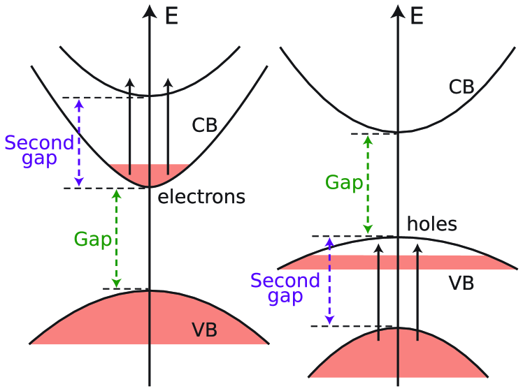
The properties of importance for a TCO are well-known (transparency, mobility, high dopability) and can be related to the fundamental electronic structure of the oxideEdwards et al. (2004); Trimarchi et al. (2011); Varley et al. (2014). This has led to an important body of computationally or chemically driven searches for good TCOs candidatesHautier et al. (2013, 2014); Scanlon and Watson (2010); Walsh et al. (2009); Kawazoe et al. (1997); Ogo et al. (2008); Yabuta et al. (2010); Perkins et al. (2011); Yan et al. (2015); Cerqueira et al. (2015). Those studies have highlighted a series of straightforward design criteria, or necessary properties for a TCO: a large band gap (ideally 3 eV), a low effective mass (of electrons for n-type and holes for p-type), and a high dopabilityZunger (2003); Scanlon et al. (2014); Robertson and Clark (2011). To achieve substantial conductivity, TCOs often present carrier concentrations on the order of 1021 cm-3. The additional electrons or holes inserted into the conduction band(CB) (for n-type TCOs) or the valence band(VB) (for p-type TCOs) can lead to new optical transitions. When interacting with incident photons, the electrons in the CB of n-type TCOs can absorb photons and undergo transitions to higher states as illustrated in the left panel of Fig. 1. In a similar way, in p-type TCOs (right panel of Fig. 1), the electrons in lower states can transition up and recombine with the holes in the VB. Such second gap transitions, may affect significantly the transparency of TCOs, and therefore appear as another key criteria for the design of transparent conductors.
In this paper, we investigate the influence of second gap transitions on the transparency of TCOs. The absorption coefficient is computed for various doping concentrations in various well-known n-type (\ceZnO, \ceIn2O3, \ceSnO2, \ceBaSnO3) and p-type TCOs (\ceCuAlO2, \ceSnO, \ceLaCuOS, \ceZnRh2O4). We show that, at large doping concentrations, the transparency can be lowered by second gap transitions and provide a quantitative estimate of the magnitude of this effect. We also point out a fundamental dissimilarity in second gap effect in many p-type TCOs compared to n-types. We relate this fundamental contrast to the very different type of chemistry present in n- versus p-type TCOs.
We use the Heyd-Scuseria-Ernzherof (HSE) hybrid exchange-correlation functional as it is known to better capture the electronic structure and especially the band gap of semiconductors and insulatorsHeyd et al. (2003); Brothers et al. (2008). Following previous works, we use a different fraction of exact-exchange for each material in order to obtain band gaps reproducing the experimental data: =25 for \ceIn2O3Walsh et al. (2008, 2009); Agoston et al. (2009), \ceBaSnO3Liu et al. (2013), \ceCuAlO2Trani et al. (2010); Scanlon and Watson (2010), and \ceZnRh2O4Scanlon and Watson (2011); =32 for \ceSnO2Varley et al. (2010) and \ceSnOVarley et al. (2013); and =37.5 for \ceZnOOba et al. (2011). For \ceLaCuOS, we are not aware of any previous HSE studies. So, we adopt a value of =25 which leads to a good agreement with experimental dataUeda et al. (2000) (see supplementary material). In order to study the optical properties, we calculate, at different carrier concentrations, the frequency-dependent dielectric tensor within the random-phase approximation (RPA)Gajdos et al. (2006) by using the VASP code Kresse and Furthmüller (1996a, b) and pymatgenOng et al. (2013) for post-treatment (more details in supplementary material).
The selected n-type and p-type TCOs cover a diverse range of chemistries. A series of information about these compounds (such as formula, space group, type of doping, computed and experimental direct band gap, etc.) is provided in Table I of supplementary material.
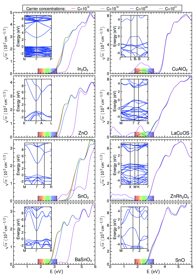
The computed absorption coefficients at different carrier concentrations (=1018-1021 cm-3) of the selected n-type materials (\ceIn2O3, \ceZnO, \ceSnO2, and \ceBaSnO3) are reported in Fig. 2 (on the left side) together with the corresponding band structures. Interestingly, increasing the carrier concentration does not lead to any absorption in the visible range. Indeed, the second gap above the CB is quite large, typically around 4 eV, and cannot lead to contributions in the visible range. In fact, for the highest carrier concentrations (1020 cm-3), the optical gap for these n-type TCOs is even widened due to the Moss-Burnstein effectGrundmann (2006). The right side of Fig. 2 shows the absorption for the selected p-type materials (\ceCuAlO2, \ceLaCuOS, \ceZnRh2O4 and \ceSnO). Significant absorption appears at low energy as the hole concentration increases. The effect is particularly large for the highest hole concentrations ( 1020 cm-3). \ceZnRh2O4, \ceCuAlO2 and \ceLaCuOS all show second gap transitions at energies lower than 3 eV. Among the p-type materials, only \ceSnO does not present a strong degradation of its transparency when the carrier concentration is increased. Indeed, the band structure of \ceSnO shows a large second gap of about 4 eV.
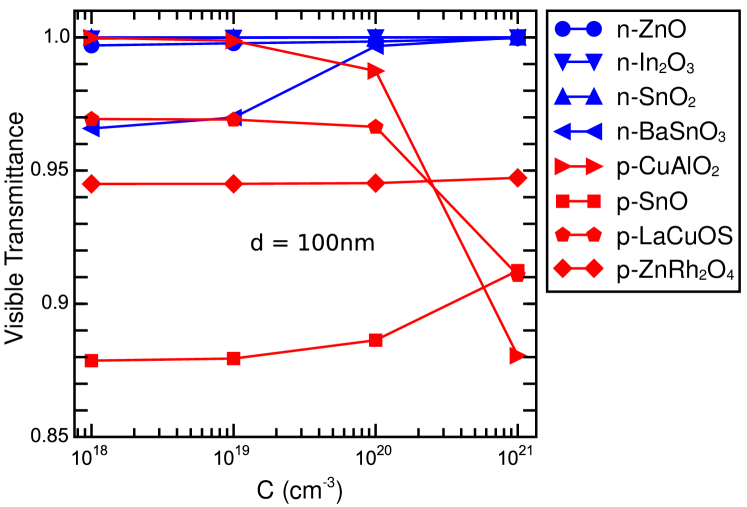
The difference between n- and p-type TCOs is striking. The n-type materials tend to have large second gap transitions that do not affect transparency when doped. In contrast, most p-type TCOs show significant absorption in the visible range due to second gap transitions with the notable exception of \ceSnO. A quantitative estimate of the effect of the second gap on the transparency is provided by the visible transmittance of a typical thin-film. Fig. 3 plots the transmittance for a 100-nm film depending on the carrier concentration. We assume here no reflection of the incident light. The blue (red) lines correspond to n-type (p-type) materials. As expected from the computed absorption coefficients, n-type TCOs do not show any degradation of their VT when the carrier concentration increases. In contrast, the transmittance of p-type TCOs is significantly degraded. This is the case for \ceCuAlO2 and \ceLaCuOS. The lower band gap of \ceZnRh2O4 induces a degradation in the transmission with doping but only in an energy window lower than the visible light (in the near infra-red). Finally, \ceSnO shows an improvement in transparency due to its large second gap combined with a Moss-Burnstein effect. We would like to stress that our analysis only takes into account direct inter-band transitions. Including also non-direct intra-band transitions Peelaers et al. (2012) would be significantly more computationally expensive. Moreover, we do not consider the loss of transmission due to the possible contribution of plasma reflectivity when carrier concentration is increased Ellmer (2012); Edwards et al. (2004). Nevertheless, our study points out to lower second gap transitions as one of the reasons explaining why many p-type TCOs show a less favorable trade-off between transparency and carrier concentration than n-type materials doZhang et al. (2015).
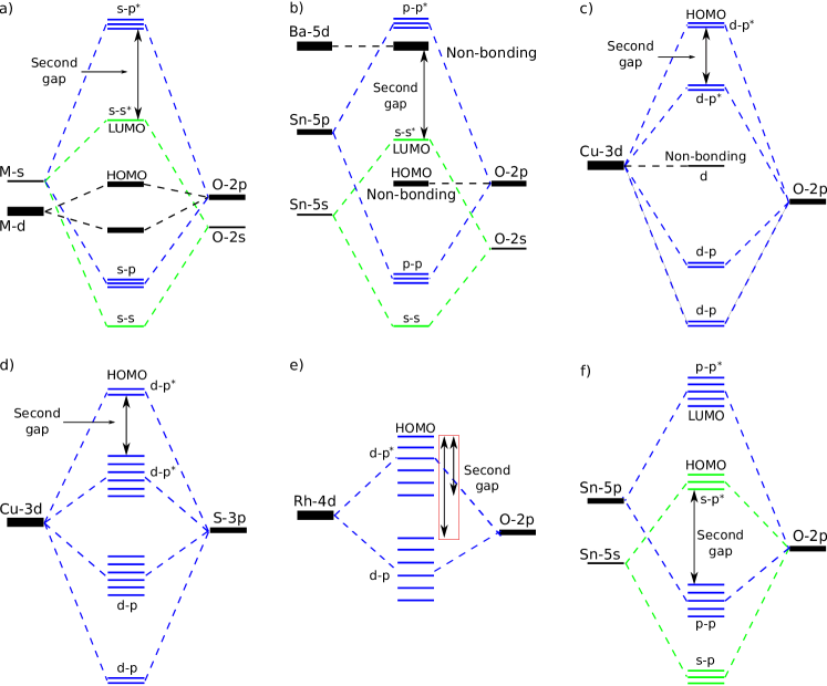
The dissimilitude between n- and p-type TCOs can be traced back to the materials chemistry. Fig. 4 shows simplified molecular orbital diagrams for the studied TCOs. The corresponding projected band structures and bonding analysis data are reported in the supplementary material. In n-type oxides (panel a), the second gap is formed by M-s/O-s and M-s/O-p anti-bonding states (with M=In, Sn or Zn) which have a large difference in energy. \ceBaSnO3 (panel b) is slightly different with the presence of a Ba-d non-bonding states but also provides a wide second gap.
The p-type TCOs on the other hand (panels c to f) show more complex orbital diagrams. The materials based on transition metals (TM) have a valence band maximum (VBM) formed by TM-d/O-p or TM-d/S-p anti-bonding states (with TM=Cu or Rh). The second gap is formed between the VBM and other TM-d/O-p, or TM-d/S-p states that are very close in energy to this VBM. This leads to small second gap transitions that can be in the visible range. In contrast, \ceSnO presents a very different character for its VBM (Sn-s/O-p) and no hybridized d-states. Hence, it shows a much larger second gap which is due to the larger hybridization of Sn-s/O-p states compared to d states to O-p. This indicates that the lower hole effective mass obtained by M-s/O-p hybridization is not only beneficial for the mobility of this compound but also for its second gap transitions. Our analysis points out to an intrinsic limit to transition d-metal-based compared to s-metal-based p-type TCOs as they not only lead to higher effective masses but also present larger limitations in terms of second gap absorption.
We give a quantitative estimate of the effect of the second gap transitions (see Fig. 3). For a 100-nm film, the observable loss in transparency with carrier concentration reached 10 at most (20 for a 200-nm film) and for the highest carrier concentrations (1020 cm-3 to cm-3). Therefore, a small second gap has a more moderate effect on transparency than the principal band gap. This comes from the smaller amount of carriers available in the small energy window corresponding to the second gap. This suggests that, while beneficial, a high second gap should not be considered a necessary condition for obtaining a working TCO.
In summary, we used ab initio calculations combined with the rigid band approximation to study the effect of heavy doping on optical absorption through “second gap” transitions. We studied a series of common n-type and p-type TCOs. A very different behavior is observed between n- and p-type materials. The n-type TCOs show high second gap transitions and do not lose transparency when highly doped. On the contrary, most p-type materials have second gap transitions lower than 3 eV which lead to a degradation of their transparency when doped. We relate the asymmetry in behavior between n- and p-type materials to their chemistry. The lower second gap present in transition metal-based p-type TCOs comes from the small energy differences between metal-O- hybridized states. Our results on \ceSnO, one of the rare non-transition metal-based p-type TCO, indicates that using p-type TCOs relying on the hybridization of O-p with metal s-states lead naturally to higher second gap transitions that are less detrimental to transparency. Our work also quantitatively estimates the effect of these second gap transitions and demonstrates that, while it is beneficial to select materials with a high second gap (3 eV ideally), the magnitude of the effect should not lead to making it a strict requirement for TCO design.
V.-A.H. was funded through a grant from the FRIA. G.-M.R. is grateful to the F.R.S.-FNRS for financial support. We acknowledge access to various computational resources: the Tier-1 supercomputer of the Fédération Wallonie-Bruxelles funded by the Walloon Region (grant agreement N0 1117545), and all the facitilies provided by the Université catholique de Louvain (CISM/UCL) and by the Consortium des Équipements de Calcul Intensif en Fédération Wallonie Bruxelles (CÉCI). The authors thank Professor Chris Van de Walle for helpful discussions.
References
- Ohta and Hosono (2004) H. Ohta and H. Hosono, Mater. Today 7, 42 (2004).
- Ellmer (2012) K. Ellmer, Nature Photon. 6, 809 (2012).
- Hamberg et al. (1984) I. Hamberg, C. G. Granqvist, K.-F. Berggren, B. E. Sernelius, and L. Engström, Phys. Rev. B 30, 3240 (1984).
- Edwards et al. (2004) P. P. Edwards, A. Porch, M. O. Jones, D. V. Morgan, and R. M. Perks, Dalton Trans. 19, 2995 (2004).
- Körber et al. (2010) C. Körber, V. Krishnakumar, A. Klein, G. Panaccione, P. Torelli, and et al., Phys. Rev. B 81, 165207 (2010).
- Mryasov and Freeman (2001) O. N. Mryasov and A. J. Freeman, Phys. Rev. B 64, 233111 (2001).
- Walsh et al. (2008) A. Walsh, J. L. F. D. Silva, S.-H. Wei, C. Körber, A. Klein, and et al., Phys. Rev. Lett. 100, 167402 (2008).
- Minami et al. (1985) T. Minami, H. Nanto, and S. Takata, Thin Solid Films 124, 43 (1985).
- Martínez et al. (1997) M. A. Martínez, J. Herrero, and M. T. Gutiérrez, Sol. Energ. Mat. Sol. Cells 45, 75 (1997).
- Aguraa et al. (2003) H. Aguraa, A. Suzukia, T. Matsushitaa, T. Aokia, and M. Okuda, Thin Solid Films 445, 263 (2003).
- Kima and Taib (2007) Y.-S. Kima and W.-P. Taib, Appl. Surf. Sci. 253, 4911 (2007).
- Ogo et al. (2008) Y. Ogo, H. Hiramatsu, K. Nomura, H. Yanagi, T. Kamiya, and et al., Appl. Phys. Lett. 93, 032113 (2008).
- Yabuta et al. (2010) H. Yabuta, N. Kaji, R. Hayashi, H. Kumomi, K. Nomura, and et al., Appl. Phys. Lett. 97, 072111 (2010).
- Kawazoe et al. (1997) H. Kawazoe, M. Yasukawa, H. Hyodo, M. Kurita, H. Yanagi, and H. Hosono, Nat. 389, 939 (1997).
- Tate et al. (2009) J. Tate, H. L. Ju, J. C. Moon, A. Zakutayev, A. P. Richard, and et al., Phys. Rev. B 80, 165206 (2009).
- Trimarchi et al. (2011) G. Trimarchi, H. Peng, J. Im, A. J. Freeman, V. Cloet, and et al., Phys. Rev. B 84, 165116 (2011).
- Varley et al. (2014) J. B. Varley, V. Lordi, A. Miglio, and G. Hautier, Phys. Rev. B 90, 045205 (2014).
- Hautier et al. (2013) G. Hautier, A. Miglio, G. Ceder, G.-M. Rignanese, and X. Gonze, Nat. Commun. 4, 2292 (2013).
- Hautier et al. (2014) G. Hautier, A. Miglio, D. Waroquiers, G.-M. Rignanese, and X. Gonze, Chem. Mater. 26, 5447 (2014).
- Scanlon and Watson (2010) D. O. Scanlon and G. W. Watson, J. Phys. Chem. Lett. 1, 3195 (2010).
- Walsh et al. (2009) A. Walsh, J. L. F. D. Silva, Y. Yan, M. M. Al-Jassim, and S.-H. Wei, Phys. Rev. B 79, 073105 (2009).
- Perkins et al. (2011) J. D. Perkins, T. R. Paudel, A. Zakutayev, P. F. Ndione, and P. A. P. et al., Phys. Rev. B 84, 205207 (2011).
- Yan et al. (2015) F. Yan, X. Zhang, Y. G. Yu, L. Yu, A. Nagaraja, and et al., Nat. Commun. 6, 7308 (2015).
- Cerqueira et al. (2015) T. F. T. Cerqueira, S. Lin, M. Amsler, S. Goedecker, S. Botti, and M. A. L. Marques, Chem. Mater. 27, 4562 (2015).
- Zunger (2003) A. Zunger, Appl.Phys. Lett. 83, 57 (2003).
- Scanlon et al. (2014) D. O. Scanlon, J. Buckeridge, C. R. A. Catlow, and G. W. Watson, J. Mater. Chem. C 2, 3429 (2014).
- Robertson and Clark (2011) J. Robertson and S. J. Clark, Phys. Rev. B 83, 075205 (2011).
- Heyd et al. (2003) J. Heyd, G. E. Scuseria, and M. Ernzerhof, J. Chem. Phys. 118, 8207 (2003).
- Brothers et al. (2008) E. N. Brothers, A. F. Izmaylov, J. O. Normand, V. Barone, and G. E. Scuseria, J. Chem. Phys. 129, 011102 (2008).
- Agoston et al. (2009) P. Agoston, K. Albe, R. M. Nieminen, and M. J. Puska, Phys. Rev. Lett. 103, 245501 (2009).
- Liu et al. (2013) H.-R. Liu, J.-H. Yang, H. J. Xiang, X. G. Gong, and S.-H. Wei, Appl. Phys. Lett. 102, 112109 (2013).
- Trani et al. (2010) F. Trani, J. Vidal, S. Botti, and M. A. L. Marques, Phys. Rev. B 82, 085115 (2010).
- Scanlon and Watson (2011) D. O. Scanlon and G. W. Watson, Phys. Chem. Chem. Phys. 13, 9667 (2011).
- Varley et al. (2010) J. B. Varley, A. Janotti, and C. G. Van de Walle, Phys. Rev. B 81, 245216 (2010).
- Varley et al. (2013) J. B. Varley, A. Schleife, A. Janotti, and C. G. Van de Walle, Appl. Phys. Lett. 103, 082118 (2013).
- Oba et al. (2011) F. Oba, M. Choi, A. Togo, and I. Tanaka, Sci. Technol. Adv. Mater. 12, 034302 (2011).
- Ueda et al. (2000) K. Ueda, S. Inoue, S. Hirose, H. Kawazoe, and H. Hosono, Appl. Phys. Lett. 77, 2701 (2000).
- Gajdos et al. (2006) M. Gajdos, K. Hummer, G. Kresse, J. Furthmüller, and F. Bechstedt, Phys. Rev. B 73, 045112 (2006).
- Kresse and Furthmüller (1996a) G. Kresse and J. Furthmüller, Comput. Mater. Sci. 6, 15 (1996a).
- Kresse and Furthmüller (1996b) G. Kresse and J. Furthmüller, Phys. Rev. B 54, 11169 (1996b).
- Ong et al. (2013) S. P. Ong, W. D. Richards, A. Jain, G. Hautier, M. Kocher, and et al., Comput. Mater. Sci. 68, 314 (2013).
- Grundmann (2006) M. Grundmann, The Physics of Semiconductors, ISBN 978-3-540-25370-9 (Springer Berlin Heidelberg New York, 2006).
- Peelaers et al. (2012) H. Peelaers, E. Kioupakis, and C. G. Van de Walle, Appl. Phys. Lett. 100, 011914 (2012).
- Zhang et al. (2015) K. H. L. Zhang, Y. Du, A. Papadogianni, O. Bierwagen, S. Sallis, and et al., Adv. Mater. 27, 5191 (2015).