Protected gap closing in Josephson junctions constructed on Bi2Te3 surface
Abstract
On the road of searching for Majorana zero modes (MZMs) in topological insulator-based Josephson junctions, a highly-sought signature is the protected full transparency of electron transport through the junctions due to the existence of the MZMs, associated with complete gap closing between the electron-like and hole-like Andreev bound states (ABSs). Here, we present direct experimental evidence of gap closing and full transparency in single Josephson junctions constructed on the surface of three-dimensional topological insulator (3D TI) Bi2Te3. Our results demonstrate that the 2D surface of 3D TIs provides a promising platform for hosting and manipulating MZMs.
I INTRODUCTION
Recently, much attention has been focused on searching for Majorana zero modes (MZMs) in condensed matter systems Majorana ; Majorana return ; Search for Majorna ; Race for Majorana . These MZMs, which could be used as topologically protected qubits, are expected to occur at the boundaries of -wave-like superconductors. Experimentally, a number of peculiar phenomena were observed and believed to relate to the occurrence of MZMs, including the appearance of a zero-bias conductance peak (ZBCP) ZBCP Kouwenhoven ; ZBCP H.Q.Xu ; ZBCP shtrikman ; ZBCP Marcus ; ZBCP van Harlingen ; ZBCP Yazdani ; ZBCP Ando ; ZBCP Marcus_2 ; ZBCP Fan Yang , the signatures of fractional Josephson effect Rokhinson ; Wiedenmann , and the emerging of skewed current-phase relations (CPRs) in related Josephson devices phase-sensitive10 and QP2 Yacoby ; Moler_PRL ; phase-sensitive7 van Harlingen NatureComm ; Pang_CPB . In the presence of MZMs, however, the ZBCP is expected to be completely quantized, and the charge transport fully transparent (i.e., perfect Andreev reflection) in related devices 4pi1 A Yu Kitaev ; 4pi2 LowTempPhy ; Fu 2008 PRL ; 4pi3 and rf1 Fu Liang 2009 PRB ; 4pi4 and rf2 nanowire ; 4pi5 and rf3 Beenakker ; current reverse and QP1 ; Fu 2013 PRB ; 4pi6 and rf4 Kane . While the complete quantization of ZBCP has been observed very recently ZBCP Hao Zhang , the complete closing of minigap between the electron-like and hole-like ABSs, as signature of fully transparent charge transport, has not yet been strictly proven.
In this work, we studied the magnetic flux-dependent evolution of the local induced minigap in single Josephson junctions constructed on the surface of three-dimensional topological insulator Bi2Te3. Our results lead to the conclusion that the minigap undergoes complete closing.
II EXPERIMENTAL METHOD AND RESULTS
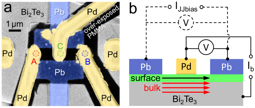
The devices used in this work were fabricated on exfoliated Bi2Te3 flakes of 100 nm in thickness. Two “T”-shape Pb pads were sputtering deposited on the surface of the flakes to define a superconductor-TI-superconductor (S-TI-S) Josephson junction. Three non-superconducting Pd electrodes were e-beam evaporated and introduced to the Bi2Te3 surface at the left, right and center of the junction (marked by A, B, and C in Fig. 1(a), respectively) for detecting the local electron states. The contacting area of each Pd electrode is defined by the windows through an over-exposed polymethyl methacrylate (PMMA) layer which was fabricated prior the deposition of the Pd electrodes, for the purpose to isolate the arms of the Pd electrodes from the Pb junction underneath. The other two Pd electrodes away from the junction were added for transport measurements. The electron transport measurements with configurations illustrated in Fig. 1(b) were performed by using lock-in amplifier technique, down to 20 mK in a dilution refrigerator. The electron temperature of the system is slightly higher, 50 mK, known from the numerical simulations for the experimental data (will be shown later).
II.1 The Josephson supercurrent between the two Pb electrodes
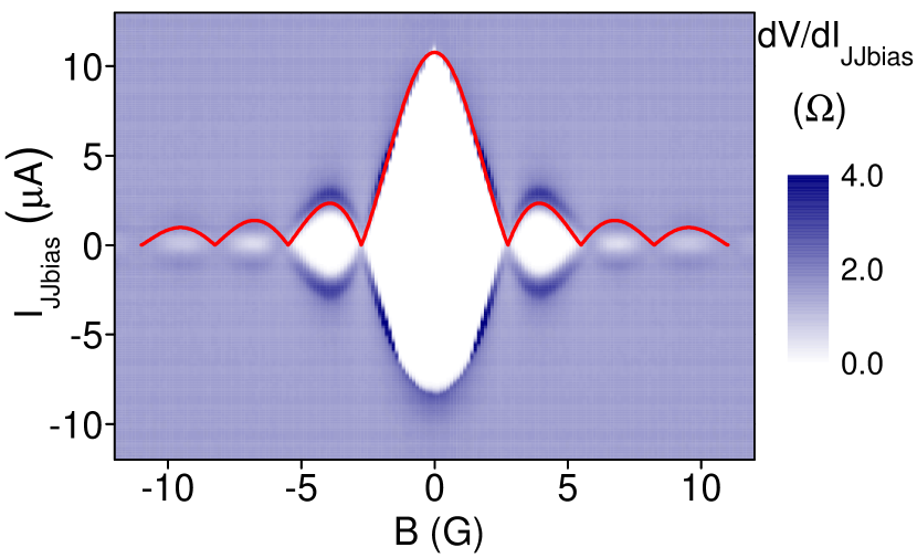
Firstly, we measured the differential resistance between the two Pb electrodes of a Pb-Bi2Te3-Pb Josephson junction (device #1), as functions of magnetic field and bias current at the base temperature. The results are shown in Fig. 2, with the bias current swept from the bottom to the top. The white-colored area represents the zero-resistance state. The pattern is slightly asymmetric along the vertical direction, as is usually seen in literature for Josephson junctions of the similar type. The envelope of the zero-resistance state along the positive bias direction agrees well with the Fraunhofer pattern of critical supercurrent for Josephson junctions in the non-transparent limit (the red curve, for further explanation please refer to the supplementary materials supplementary_materials ). The period of the Fraunhofer pattern is G. It corresponds to an effective junction area of m2 (where is flux quantum, the electron charge, and the Planck constant). This estimated area is in good agreement with the geometric area of the junction m2, where is the width and the effective distance between the two Pb electrodes after considering flux penetration and compression supplementary_materials .
II.2 The contact resistance in the junction area probed by Pd electrods
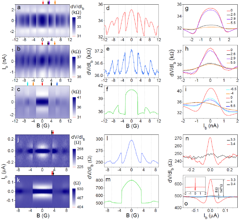
Then, we measured the contact resistance of the Pd electrodes by employing a three-terminal configuration as illustrated in Fig. 1(b), to probe the local electron states in the junction area. The measurement current was kept 1/1000 of the critical supercurrent of the Josephson junction, to avoid disturbing the status of the Josephson junction. Figures 3(a), (b) and (c) show the 2D color plots of the contact resistance on device #1 at positions A, B and C, respectively, as functions of and bias current . In contrast to the continuous variation of the Fraunhofer pattern shown in Fig. 2, the contact resistance of all contacts exhibits sharp jumps when is swept across the nodes of the Fraunhofer pattern. These sharp jumps can also be clearly seen from the horizontal line cuts of the 2D plots. The line cuts of Figs. 3(a) and (b) at , plotted in Figs. 3(d) and (e) respectively, show a skewed dependence followed by abrupt jumps. And the line cut of Fig. 3(c) at , plotted in Fig. 3(f), shows a square-shape dependence before rectified by the Fraunhofer-like envelope.
In Figs. 3(g), (h) and (i) we plot the vertical line cuts taken at different in the corresponding 2D plots. It can be seen that a gap-like structure on curves undergoes sudden opening/closing with varying at the Fraunhofer nodes (i.e., jumping between curves with most pronounced gap structures to least pronounced ones). We will show later that the remaining tiny signature of gap after gap closing, i.e., those on the black and the orange curves in Figs. 3(g), (h) and (i), is caused by the finite size effect of the Pd electrodes.
The contact resistance of Pd electrodes in device #1 was higher than the quantum unit k, indicating that the measurement was in the tunneling regime, so that the results reflect mostly the information of the electron density of states underneath. We have fabricated and measured more than ten devices. Similar results were obtained even when the contact resistance of Pd electrodes was in a range below the quantum unit , presumably because multiple tunneling channels shunt together in the contacting area. Figures 3(j)–(o) give such an example.
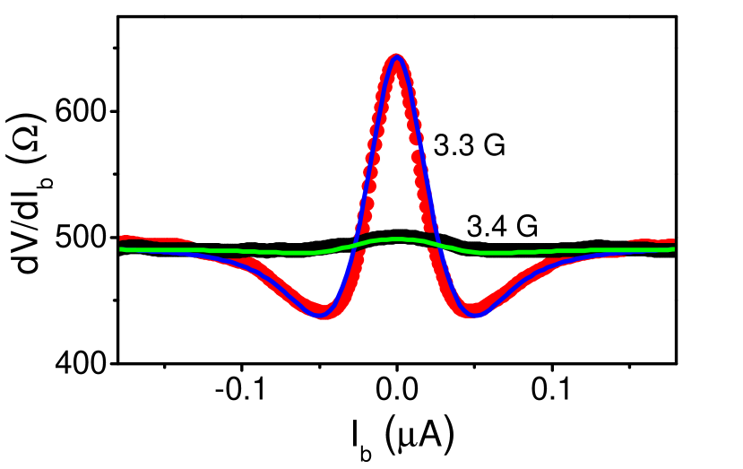
Gap closing can be most clearly seen in the main frame and the inset of Fig. 3(o), where the normal-state value of can be firmly determined and is represented by the horizontal blue line. It can be seen that 95% of the peak height suddenly vanishes upon gap closing, i.e., from 147 at 3.3 G to 8 at 3.4 G.
Gap closing can also be seen in Figs. 3(d), (e), (f), (i) and (m). The line cuts in these plots, which represent the field-dependent peak height of the curvrs, approach to the normal-state values at their oscillatory minimums.
III DISCUSSIONS
III.1 The phase dependence of superconducting minigap
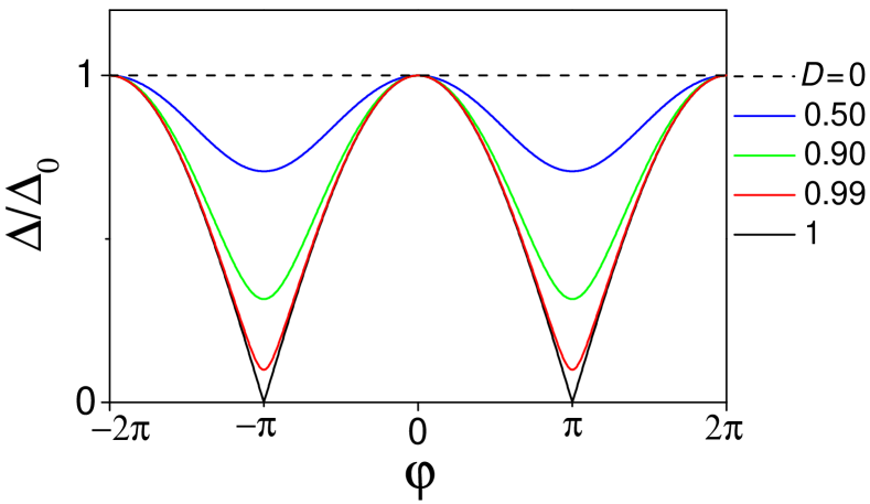
That the contact resistance and the Fraunhofer pattern of supercurrents share the same oscillation period implies that the oscillation is controlled by the same phase difference across the junction. It is known for S-N-S type Josephson junctions (where N denotes normal metals) that the backwards and forwards Andreev reflections between the two S-N interfaces lead to the formation of ABSs in the N. The minigap in the junction area, which is the level spacing between the lowest-energy electron-like and hole-like ABSs, shall oscillate with Beenakker_full_trans :
| (1) |
where is the maximal value of the minigap, is the total transmission coefficient of the junction, including those of the two S-N interfaces and that of the N part.
The oscillation of with varying is depicted in Fig. 4. It can be seen that the more transparent the junction is, the more oscillatory the minigap will be. But it is very difficult to reach full gap-closing — the minigap remains significantly open even if the total transmission coefficient is as high as 0.99 (the red curves).
The local phase difference in Eq. 1 is controlled by the magnetic flux in the junction area:
| (2) |
where is the total magnetic flux in the junction of area , and is defined from to . The first term in Eq. 2 is the local phase difference caused by magnetic flux. The second term represents a phase jump whenever the total flux in junction crosses the nodes of the Fraunhofer pattern.
For the mechanism of phase jump, it is well known that for single Josephson junctions there exists a phase offset which can be self-adjusted to minimize the total energy. As can be seen in the supplementary materials supplementary_materials , in the flux range of the 0th Fraunhofer peak, the lowest-energy state corresponds to the state. But in the flux range of the 1st Fraunhofer peak, the lowest-energy state corresponds to the state. A phase jump will thus take place at the nodes of the Fraunhofer pattern.
III.2 Transparent or non-transparent? Dilemma and solution
As illustrated in Fig. 4, the minigap is less oscillatory with varying magnetic flux when (the non-transparent limit), but becomes most oscillatory when (the transparent limit). The observation of significant oscillation rules out that our Josephson junction is in the non-transparent limit — a conclusion which is in sharp contrast to the one drawn from the Fraunhofer pattern in Fig. 2. To solve this dilemma, we have to believe that there exist two distinct CPRs, corresponding to two different supercurrents as illustrated in Fig. 1(b). One CPR corresponds to the majority supercurrent flowing through the bulk of Bi2Te3 in the non-transparent limit Qu_SR , resulting in the measured Fraunhofer pattern of the non-transparent type. The other CPR corresponds to the supercurrent flowing through highly transparent channels, presumably the ABSs on the surface of Bi2Te3. The contact resistance depends sensitively on the surface electron density of states, hence a highly oscillatory was detected.
In the transparent limit , Eq. 1 becomes:
| (3) |
In this limit, the minigap undergoes complete closing at the Fraunhofer nodes.
In the next sections, we will analyze the data of the contact resistance quantitatively and qualitatively, to convince the readers that the minigap undergoes completely closing and that our Josephson junctions are indeed fully transparent.
III.3 Simulation of the curves by using the BTK theory
Although the significant oscillation of the contact resistance infers that the Pb-Bi2Te3-Pb Josephson junctions are in the transparent limit, the high value of the contact resistance itself tells that the transport process across the Pd-Bi2Te3 interface is rather non-transparent. We note that there was no intentionally made barrier at this interface. The remnant photoresist on the Bi2Te3 surface, if present, is 1 nm thick or less as revealed by atomic force microscopy studies. Such an interface should allow the happening of direct tunneling of single quasiparticles as well as the two-particle Andreev reflection process. These processes are usually described by the Blonder-Tinkham-Klapwijk (BTK) theory BTK .
It is not quite straightforward that the BTK theory can be applied to describe the single-particle and two-particle processes across the Pd-Bi2Te3 interface here, since the superconducting gap in Bi2Te3 is not a standard one but an induced minigap between the lowest-energy electron-like and hole-like Andreev bound states (or continuums in the dirty regime). Nevertheless, while the electron-like and hole-like ABSs (or continuums) at the Bi2Te3 surface mediate the Josephson supercurrents between the two Pb electrodes, the same ABSs (or continuums) also define an energy window within which the two-particle process can occur between the Pd electrode and the superconducting bath (e.g., firstly to the superconducting bulk of Bi2Te3 Qu_SR , then eventually to the Pb electrodes). Although a rigours theory is still needed to treat this special case, our numerical simulation below demonstrates that the BTK formalism works well to describe the single-particle and two-particle processes across the Pd-Bi2Te3 interface.
For a single conduction channel connecting a normal metal reservoir N and a superconductor reservoir S, the current can be expressed as:
| (4) |
where is the quantum conductance, is the normal (electron-to-electron) reflection coefficient to suppress the current, is the Andreev (electron-to-hole) reflection coefficient to increase the current, and is the Fermi distribution function of the left/right reservoirs.
According to the BTK theory:
| (5) | ||||
where is the minigap determined by the total transmission coefficient of the Pb-Bi2Te3-Pb Josephson junction via Eq. 1, and is the barrier strength of the Pd-Bi2Te3 interface, related to the transmission coefficient of the interface via .
In the real case, there exist multiple channels at the Pd-Bi2Te3 interface. For simplicity, we assume that the transmission coefficient of each channel is the same. The total current is then:
| (6) |
where is the number of parallel channels.
With the above formula, we can simulate the curve, the curve, as well as the curve of the Pd-Bi2Te3 interface. Figure 5 shows the simulations on the data of device #2 shown in Fig. 3(o). The fitting parameters are , and mK. The minigap is 9.25 V before closing at G (the blue line), and 1.8 V after closing at G (the green line). The large height reduction of the gap structure yields a very high transmission coefficient of for the Pb-Bi2Te3-Pb Josephson junction. This value of is comparable to that of a single-atomic-layer Josephson junction G. H. Lee and an atomic superconducting point contact Rocca . It is in sharp contrast to the transmission coefficient of the Pd-Bi2Te3 interface of the central Pd electrode in device #2, where and hence the transmission coefficient is only .
III.4 The finite-size effect of the Pd electrodes
In the above simulation we assume that the Pd electrode is a geometric point. In the real case, however, the Pd electrode always picks up signals within an area where the minigap remains unclosed at most places, such that the measured signature of gap closing is largely diminished. In other words, the true minigap at the center of the junction should be much smaller than 1.8 V when the magnetic flux reaches the Fraunhofer nodes. We therefore believe that the total transmission coefficient of our S-TI-S junction is much higher than 0.96, being already in the fully transparent limit.
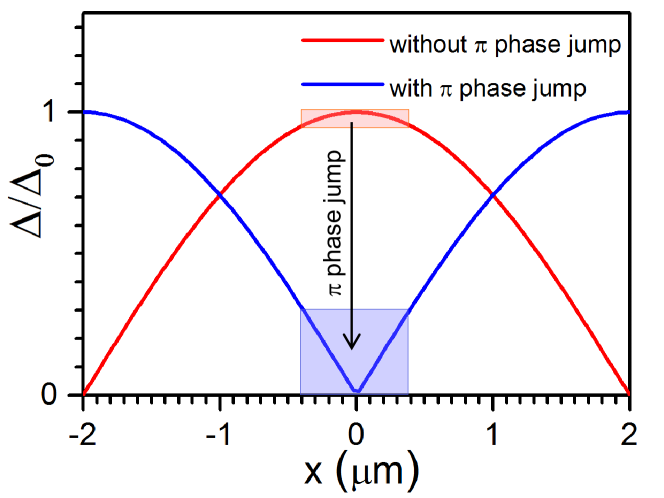
In the following, we demonstrate that the remaining gap structure on the black/green curves in Fig. 5 can be well ascribed to the finite-size effect of the Pd electrode while complete gap closing already occurs at . From Eqs. 2 and 3, the position dependence of the minigap in the full transparent limit can be calculated. The results before and after phase jump in the vicinity of the first Fraunhofer node are plotted in Fig. 6. It can be seen that strict gap closing takes place only at the ends of the junction before the phase jump, and at the center after the phase jump. Obviously, the central Pd electrode of device #2 with width 800 nm illustrated by the light blue rectangle in Fig. 6 picks up not only the gap-closing signal at the center of the junction, but also the gap-opening signal in the vicinity area. Therefore, the measured signature of gap closing in real experiment is diminished by the finite size effect.
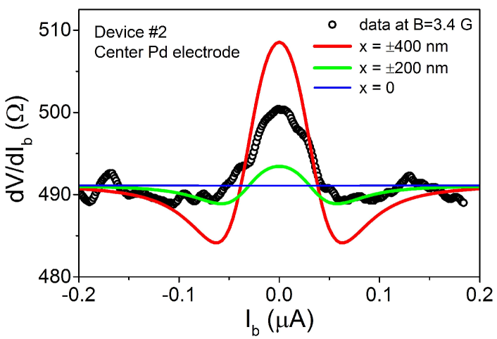
In Fig. 7 we show the curves at 200 nm and 400 nm expected in the fully transparent limit, in comparison with the experimental data at G taken from the central Pd electrode of device #2 whose diameter is 800 nm. The results unambiguously show that the remaining tiny feature of gap in the experimental data can be a finite-size effect of the Pd electrode.
III.5 Simulations of the magnetic flux dependencies of zero-bias in the fully transparent limit and after taking into account the finite-size effect of the Pd electrodes
Taking the finite-size effect of the Pd electrodes into account, we can further simulate the magnetic flux dependence of the data in the fully transparent limit .
Because the superconducting gap underneath the Pd electrode varies specially, the normal-reflection coefficient and the Andreev-reflection coefficient are functions of position . The total current can be rewritten as:
| (7) |
where is the number of channels per unit area (i.e., channel density). For simplicity, we assume the channel density is a constant . The formula becomes:
| (8) |
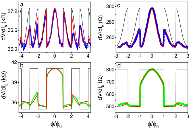
With Eqs. 5 and 8, the magnetic field dependence of can be simulated. Plotted in Figs. 8(a), (b), (c) and (d) are the simulations to the experimental data shown in Figs. 3(e), (f), (l) and (m), respectively. The blue and green dots are the experimental data. The black lines are the simulations assuming zero-sized electrodes located strictly at (the ends) or (the center). The red lines in Figs. 8(a) and (b) are the simulations for electrodes of diameter 600 nm at the end and 660 nm at the center of device #1, respectively. And the red lines in Figs. 8(c) and (d) are the simulations for electrodes of diameter 770 nm at the end and 800 nm at the center of device #2, respectively. The excellent agreement between the data and the simulations supports the conclusion that the Pb-Bi2Te3-Pb junctions are in the fully transparent limit, and that complete gap closing indeed occurs.
III.6 Further discussions
The total transmission coefficient of an Pb-TI-Pb Josephson junction relies on the transmission coefficients of the two Pb-TI interfaces and that of the TI part. Although in this experiment we did not measure the barrier strength of single Bi2Te3-Pb interfaces, our early study on Bi2Se3-Sn interfaces prepared via the same techniques shows that the barrier strength is not close to 0 at all, but remaining as high as 0.6 even after additional reactive ion etching was applied to reduce the remnant photoresist ZBCP Fan Yang . If taking , single Bi2Te3-Pb interface yields a transmission coefficient of , being already significantly smaller than 1. In addition to the interface scattering, the Bi2Te3 part in our junction is 1 m in length. We therefore conclude that full transparency of quasiparticle transport in our Pb-Bi2Te3-Pb junctions could hardly be observed if without a mechanism to prohibit the happening of backscatterings. It is due to the single-helicity nature of the surface states that the backscatterings are completely suppressed and perfect Andreev reflections are enabled between the two Bi2Te3-Pb interfaces, leading to the formation of MZMs when phase difference is reached. In contrast, the charge transport along the perpendicular direction across the Pd-Bi2Te3 interface has nothing to do with the zero mode formation, and thus is not protected to be fully transparent. In fact, the barrier strength of single Pd-Bi2Te3 interface ranges from 2.1 to 6.9 in this experiment (see the fitting parameters in Fig. 8). Taking the central Pd electrode of device #2 as an example, whose , its transmission coefficient is only .
IV SUMMARY
We have performed contact resistance measurement on single Josephson junctions constructed on Bi2Te3 surface. Complete gap closing is inferred from the data, indicating the existence of topologically protected full transparency of charge transport through the surface states of Bi2Te3. Our results support the Fu-Kane proposal that Majorana zero modes can be hosted in Josephson junctions constructed on the 2D surface of 3D TIs. Based on such a 2D platform, universal topological quantum computation could be further implemented FuPRX .
Note added: The first version of this paper was posted on arXiv (arXiv:1603.04540v1). During revision we noticed that a similar work was recently carried out by Schüffelgen and coworkers boosting , in which the authors show that for a Nb-Bi2Te3-Nb Josephson junction containing a few tens nm of Bi2Te3 in length, the total transmission coefficient is as high as 0.95.
Acknowledgments We would like to thank L. Fu, G. M. Zhang, T. Xiang, X. C. Xie, Q. F. Sun, R. Du, Z. Fang, X. Dai, X. Hu and Z. G. Cheng for fruitful discussions. This work was supported by the National Basic Research Program of China from the MOST grants 2016YFA0300601, 2017YFA0304700, 2015CB921402, 2011CB921702 and 2009CB929101, by NSFC grants 11527806, 91221203, 11174340, 11174357, 91421303, 11774405 and by the Strategic Priority Research Program B of the Chinese Academy of Sciences grant No. XDB07010100.
References
- (1) E. Majorana, Nuovo Cimento 14, 171-184 (1937).
- (2) F. Wilczek, Nature Phys. 5, 614-618 (2009).
- (3) R. F. Service, Science 332, 193-195 (2011).
- (4) M. Franz, Physics 3, 24 (2010); M. Franz, arXiv: 1302.3641v1.
- (5) V. Mourik, K. Zuo, S. M. Frolov, S. R. Plissard, E. P. A. M. Bakkers, and L. P. Kouwenhoven, Science 336, 1003-1007 (2012).
- (6) M. T. Deng, C. L. Yu, G. Y. Huang, M. Larsson, P. Caroff, and H. Q. Xu, Nano Lett. 12, 6414-6419 (2012).
- (7) A. Das, Y. Ronen, Y. Most, Y. Oreg, M. Herblum, and H. Shtrikman, Nature Phys. 8, 887-895 (2012).
- (8) H. O. H. Churchill, V. Fatemi, K. Grove-Rasmussen, M. T. Deng, P. Caroff, H. Q. Xu, and C. M. Marcus, Phys. Rev. B 87, 241401 (2013).
- (9) A. D. K. Finck, D. J. Van Harlingen, P. K. Mohseni, K. Jung, and X. Li, Phys. Rev. Lett. 110, 126406 (2013).
- (10) S. Nadj-Perge, I. K. Drozdov, J. Li, H. Chen, S. Jeon, J. Seo, A. H. MacDonald, B. A. Bernevig, and A. Yazdani, Science 346, 602-607 (2014).
- (11) S. Sasaki, M. Kriener, K. Segawa, K. Yada, Y. Tanaka, M. Sato, and Y. Ando, Phys. Rev. Lett. 107, 217001 (2011).
- (12) M. T. Deng, S. Vaitiekenas, E. B. Hansen, J. Danon, M. Leijnse, K. Flensberg, J. Nygård, P. Krogstrup, and C. M. Marcus, Science 354, 6319 (2016).
- (13) F. Yang, Y. Ding, F. Qu, J. Shen, J. Chen, Z. Wei, Z. Ji, G. Liu, J. Fan, C. Yang, T. Xiang, and L. Lu, Phys. Rev. B 85, 104508 (2012).
- (14) L. P. Rokhinson, X. Liu, and J. K. Furdyna, Nature Phys. 8, 795-799 (2012).
- (15) J. Wiedenmann, E. Bocquillon, R. S. Deacon, S. Hartinger, O. Herrmann, T. M. Klapwijk, L. Maier, C. Ames, C. Brüne, C. Gould, A. Oiwa, K. Ishibashi, S. Tarucha, H. Buhmann, and L. W. Molenkamp, Nature Commun. 7, 10303 (2016).
- (16) S. P. Lee, K. Michaeli, J. Alicea, and A. Yacoby, Phys. Rev. Lett. 113, 197001 (2014).
- (17) I. Sochnikov, L. Maier, C. A. Watson, J. R. Kirtley, C. Gould, G. Tkachov, E. M. Hankiewicz, C. Brüne, H. Buhmann, L. W. Molenkamp, and K. A. Moler, Phys. Rev. Lett. 114, 066801 (2015).
- (18) C. Kurter, A. D. K. Finck, Y. S. Hor, and D. J. Van Harlingen, Nature Commun. 6, 7130 (2015).
- (19) Y. Pang, J. Wang, Z. Z. Lyu, G. Yang, J. Fan, G. T. Liu, Z. Q. Ji, X. N. Jing, C. L. Yang, and Li Lu, Chin. Phys. B 25, 117402 (2016).
- (20) A. Yu Kitaev, Phys.-Usp. 44, 131 (2001).
- (21) H. J. Kwon, V. M. Yakovenko, and K. Sengupta, Low Temp. Phys. 30, 613 (2004).
- (22) L. Fu and C. L. Kane, Phys. Rev. B 79, 161408 (2009).
- (23) R. M. Lutchyn, J. D. Sau, and S. Das Sarma, Phys. Rev. Lett. 105, 077001 (2010).
- (24) M. Diez, I. C. Fulga, D. I. Pikulin, M. Wimmer, A. R. Akhmerov, and C. W. J. Beenakker, Phys. Rev. B 87, 125406 (2013).
- (25) B. J. Wieder, F. Zhang, and C. L. Kane, Phys. Rev. B 89, 075106 (2014).
- (26) C. W. J. Beenakker, D. I. Pikulin, T. Hyart, H. Schomerus, and J. P. Dahlhaus, Phys. Rev. Lett. 110, 017003 (2013).
- (27) L. Fu and C. L. Kane, Phys. Rev. Lett. 100, 096407 (2008).
- (28) A. C. Potter and L. Fu, Phys. Rev. B 88, 121109 (2013).
- (29) H. Zhang, C. -X. Liu, S. Gazibegovic, D. Xu, J. A. Logan, G. Wang, N. van Loo, J. D. S. Bommer, M. W. A. de Moor, D. Car, R. L. M. O. het Veld, P. J. van Veldhoven, S. Koelling, M. A. Verheijen, M. Pendharkar, D. J. Pennachio, B. Shojaei, J. S. Lee, C. J. Palmstrøm, E. P. A. M. Bakkers, S. Das Sarma, L. P. Kouwenhoven, Nature doi:10.1038/nature26142.
- (30) See Supplemental Material at [URL will be inserted by publisher] for more discussions.
- (31) C. W. J. Beenakker, Transport phenomena in Mesoscopic Systems, H. Fukuyama and T. Ando, eds. Springer, Berlin (1992).
- (32) F. Qu, F. Yang, J. Shen, Y. Ding, J. Chen, Z. Q. Ji, G. T. Liu, J. Fan, X. N. Jing, C. L. Yang and L. Lu, Sci. Rep. 2, 339 (2012).
- (33) G. E. Blonder, M. Tinkham, and T. M. Klapwijk, Phys. Rev. B 25 , 4515 (1982).
- (34) G. H. Lee, S. Kim, S. H. Jhi, and H. J. Lee, Nature Commun. 6, 6181 (2015).
- (35) M. L. Della Rocca, M. Chauvin, B. Huard, H. Pothier, D. Esteve, and C. Urbina, Phys. Rev. Lett. 99, 127005 (2007).
- (36) S. Vijay, T. H. Hsieh, and L. Fu, Phys. Rev. X 5, 041038 (2015).
- (37) P. Schüffelgen, Da. Rosenbach, C. Li, T. Schmitt, M. Schleenvoigt, A. R. Jalil, J. Kölzer, M. Wang, B. Bennemann, Um. Parlak, L. Kibkalo, M. Luysberg, G. Mussler, A. A. Golubov, A. Brinkman, T. Schäpers, D. Grützmacher, arXiv:1711.01665.
See pages ,- of Supplementary_information_single_JJ_PRB180621