Diffusion-driven growth of nanowires by low-temperature molecular beam epitaxy.
Abstract
With ZnTe as an example, we use two different methods to unravel the characteristics of the growth of nanowires by gold-catalyzed molecular beam epitaxy at low temperature. In the first approach, CdTe insertions have been used as markers, and the nanowires have been characterized by scanning transmission electron microscopy, including geometrical phase analysis, and energy dispersive electron spectrometry; the second approach uses scanning electron microscopy and the statistics of the relationship between the length of the tapered nanowires and their base diameter. Axial and radial growth are quantified using a diffusion-limited model adapted to the growth conditions; analytical expressions describe well the relationship between the NW length and the total molecular flux (taking into account the orientation of the effusion cells), and the catalyst-nanowire contact area. A long incubation time is observed. This analysis allows us to assess the evolution of the diffusion lengths on the substrate and along the nanowire sidewalls, as a function of temperature and deviation from stoichiometric flux.
Keywords: nanowires, molecular beam epitaxy, electron microscopy, ZnTe, EDX.
I introduction
The core-shell nanowire (NW) configuration is extremely flexible and virtually any material combination, with any mismatch (up to a critical thickness which can be large)Nazarenko or no mismatch, can be realized. A first, obvious application in semiconductor materials is the fabrication of a shell with a larger bandgap in order to reduce the effect of surface defects on the properties of carriers confined in the core.demichel ; joyce A tapered (cone-shaped) configuration may even be tailored to improve light extraction.claudon A natural extension is a dot embedded in a NW, where the shape of the insertion controls the confinement of the carriers - electrons and holes. Many opportunities are then opened for a precise engineering of the envelope functions, not only through the natural band offsets, but also through a proper design of the built-in strain and the associated piezoelectric field and deformation potential.Niquet ; Boxberg ; Ferrand In particular, it allows one to engineer the hole states in a semiconductor dot and tailor their orbital and spin states: a flat insertion induces a strain configuration (hence a light-hole heavy-hole splitting) quite similar to that of a dot made of the same materials but grown by the Stranski-Krastanov mechanism, while the configuration is reversed in a core-shell NWFerrand or an elongated dot. This opens the opportunity to fully design the photonic properties of the nanostructure, and its magnetic properties if magnetic impurities are added.
To grow a well-controlled core-shell structure, two different strategies can be implemented: (1) start with the growth of the core under conditions which favor the diffusion of adatoms on the sidewalls and therefore the axial (or longitudinal) growth, then change the growth conditions in order to enhance the radial growth and form the shell. For instance, the substrate temperature is decreased between the core and shell growth steps. (2) use conditions where a moderate diffusion occurs along the sidewalls, allowing that both axial and radial growth occur simultaneously, resulting in cone-shaped (tapered) structures; this can be achieved using the same, moderately low temperature for the growth of the whole structure.
In the present study we describe the growth mechanisms of ZnTe NWs and CdTe-ZnTe structures by molecular beam epitaxy (MBE). The specific properties of II-VI materials can be fully exploited in such heterostructured NWs, with applications in photonics, photodetectors,Meng09 single photon emitters,Bounouar photovoltaicsPV including type-II configurations, various sensors, and magnetic objects.Wojn12 In the case of tellurides, (Zn,Mg)Te shells have been shown to enhance the photoluminescence efficiency by several orders of magnitude with respect to that of bare ZnTe NW.Artioli2013 Moreover, previous studies of heterostructured NWs based on tellurides (of Cd, Zn, Mg, Mn) suggest that they offer a great flexibility in their design in order to control the light-hole / heavy-hole character of the confined ground state of holes.Wojn12 ; Artioli2013 ; Szymura ; Ferrand ; Artioli2015 ; Jeannin A low growth temperature (C) was chosen to minimize the desorption of adatoms, particularly in view of the insertion of CdTe segments in the ZnTe NWs. We obtain tapered NWs with smooth sidewalls, and a well controlled insertion of CdTe and (Cd,Mn)Te. Characteristic parameters are extracted using the analytical results of a model of diffusion-limited growth; their dependence on growth temperature and stoichiometry, and on the shape of the gold nanoparticle, is discussed.
The paper is organized as follows: the experimental results are described in section II and used in section III to extract significant parameters of a diffusion-limited model of growth adapted to our findings (presented in the appendix). Section IV discusses the main aspects of the growth and their consequences.
II Experimental
II.1 Experimental methods and growth conditions
Our MBE system comprises a Riber 32P II-VI chamber connected under UHV to a Meca2000 III-V chamber equipped with As and Au effusion cells. The sample temperatures are measured by a thermocouple in direct contact with the molybdenum sample-holder. Beam equivalent pressures (BEP) were converted into flux ratios as described in Ref. Rueda2014, and checked using reflection high-energy electron diffraction (RHEED) oscillations. An important parameter for the growth of NWs, is the angle of each effusion cell with respect to the normal to the substrate: this angle determines the ratio of average flux impinging onto the facets of a normal NW to the flux impinging onto the substrate: . In our system, the values are for CdTe and Mn, for ZnTe and Mg, for Te and for Cd and Zn.
Unless otherwise mentioned, a typical growth sequence consisted in the deoxidation of the (111)B GaAs substrate at C under As flux (1 10-5 torr), the growth of a 250-500 nm-thick ZnTe buffer layer at C under stoichiometric ZnTe flux, annealing at C under Te flux, the deposition of a submonolayer gold layer at room temperature in the III-V chamber. Gold seeds were formed by dewetting at C during 5 min in the II-VI chamber. Then the sample rotation was started and the NW growth initiated immediately at the same temperature. Monitoring each step by RHEED allows us to check the characteristic features of a good quality growth: and reconstruction of the GaAs surface, Yang c(8x4) and R surface reconstruction of smoothed ZnTe layers,RuedaDewett ; RuedaPhD and formation of a Au-induced R surface reconstruction.RuedaDewett ; RuedaPhD
NWs deposited on a holey carbon-coated copper grid were imaged by energy dispersive x-ray (EDX) spectrometry using a FEI Tecnai Osiris scanning transmission electron microscope equipped with four silicon 157 drift detectors, as described in Ref. RuedaEDX, . Other NWs, still standing on the substrate, were imaged by scanning electron microscopy (SEM) using a Zeiss U55 operated at 10 keV, with a spatial resolution around 1 nm. Selected NWs, attached to the substrate in the cleaved sample geometry,MdH were imaged by scanning transmission electron microscopy (STEM) on a probe corrected FEI Titan working at 300 kV, and the lattice spacing in the high resolution images was analyzed by the geometrical phase analysis (GPA) hytchGPA . Scan noise was removed from the images by using the unperturbed ZnTe lattice as a reference.rouviereGPA
II.2 Experimental results
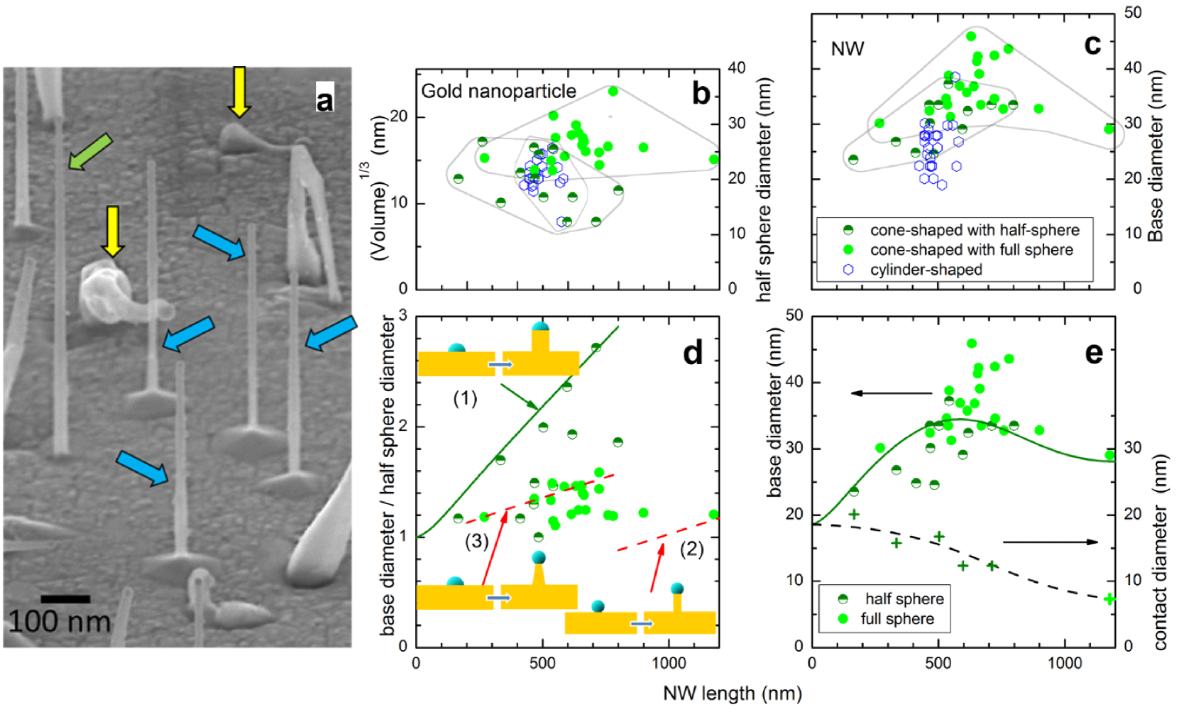
Two types of ZnTe NW can be grown: cone-shaped (tapered) NWs, and cylinder-shaped NWs, as indicated by the green and blue arrows, respectively, in the inset of Fig. 1. The main characteristicsRueda2014 of cone-shaped NWs are the zinc-blende structure with the NW axis parallel to the direction, a significant lateral growth on the sidewalls (formed by facets visible for thick enough NWs) and a crater surrounding the base of the NW. In contrast, cylinder-shaped NWs exhibit the wurtzite structure with the NW axis along the c-axis, no contribution from lateral growth detected and a pyramid at the base of the NW clearly visible in the inset of Fig. 1. The flux on the substrate far away from any NW results in the growth of a two-dimensional layer: its thickness was determined from the SEM observation of a cleaved edge.
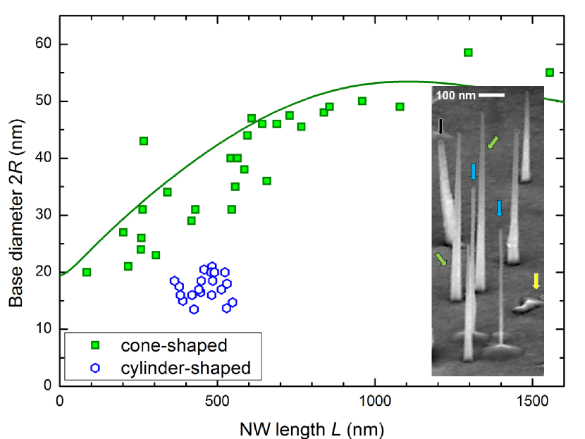
As shown in the plot of Fig. 1, the wurtzite NWs are characterized by a reasonably compact distribution of their length, and of the base diameter (which actually fairly matches the typical gold particle diameter). This is in sharp contrast with the statistics on the zinc-blende NWs: (1) except for the shorter NWs, the base diameter increases significantly; (2) we observe a broad distribution of their length, with one order of magnitude between the longest and the shortest NWs; (3) there is a clear trend suggesting a correlation between the base diameter and the NW length.
Such a large dispersion cannot be explained by the distribution of gold particle size (we did not observe any significant difference in the external diameter of the gold particle present at the tip of different NWs), or by the molecular flux. In the following we will (1) use CdTe markers to reveal the presence of an incubation time, (2) analyse the distribution obtained when growing at higher temperature to reveal the role of the shape and size of the gold nanoparticle, and (3) use a model adapted to the present growth conditions, which is amenable to analytical expressions, to examine the role of adatom diffusion.
II.2.1 CdTe markers
In order to obtain precise information on a single NW, we used a marker technique:marker1 ; marker2 we inserted 10 thin CdTe markers (stoichiometric Cd+Te flux from the CdTe cell) during the growth of a ZnTe NW sample (stoichiometric Zn+Te flux from the ZnTe cell), see Fig. 2a. The EDX image of a NW deposited on a grid (Fig. 2b) clearly reveals 7 regularly spaced CdTe insertions (and another one at the broken end). On such a broken NW, we cannot exclude that the two missing insertions were lost in the harvesting process.
In order to rule out any effect of harvesting, as-grown NWs from the same sample, still on the substrate, have been visualized by TEM, and two cone-shaped NWs very different in length (520 and 70 nm respectively) have been analyzed by GPA. The zinc-blende structure was confirmed for both NWs.
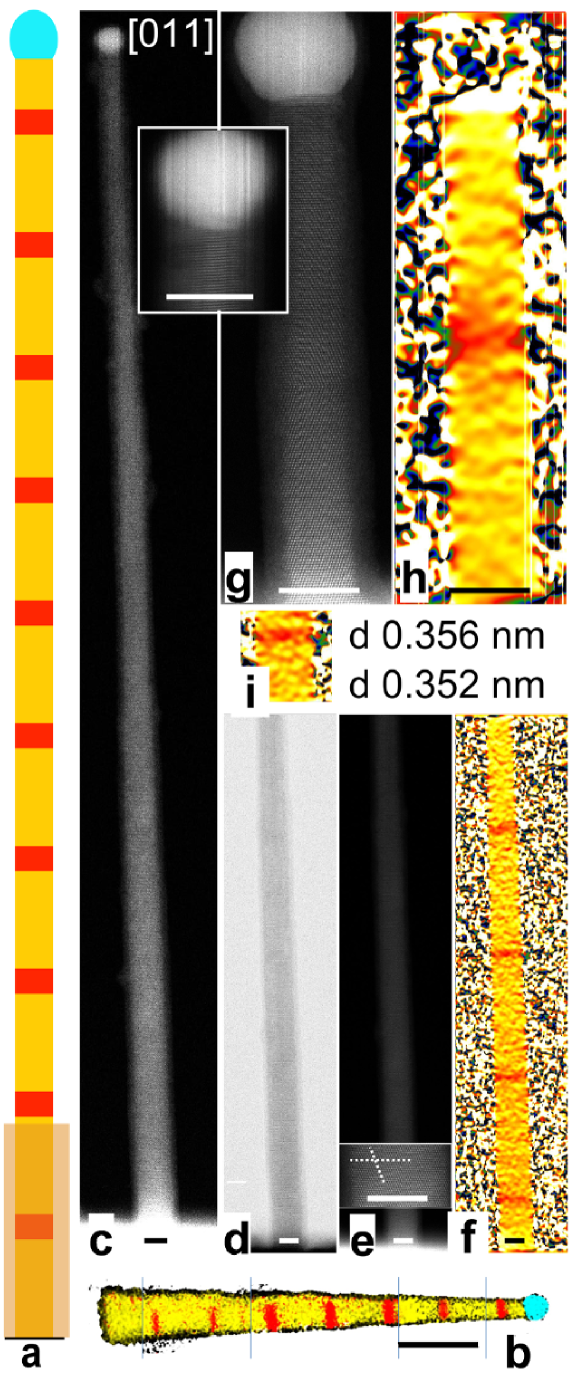
The topmost half of the longer NW (NW1 in Fig. 2c-f) could not be analyzed due to vibrations and charging effects. In the lower half, four CdTe insertions are clearly identified (Fig. 2f). The period is 68 nm, with 64 nm for the ZnTe spacers and 4 nm for the CdTe insertions: this ratio is in good agreement with the ratio of integrated lateral flux, which was ZnTe:CdTe15, suggesting that the growth of this part of the NW is mainly governed by the adatoms resulting from the flux to the sidewalls and diffusing to the gold nanoparticle. This preponderant role of the lateral flux is confirmed by the plot of the length of CdTe and ZnTe components of various heterostructured NWs grown using molecular beams with very different angles of incidence (Fig. 3a).
On the shorter NW (NW2 in Fig. 2g,h), only one CdTe insertion is identified, suggesting a long incubation time.
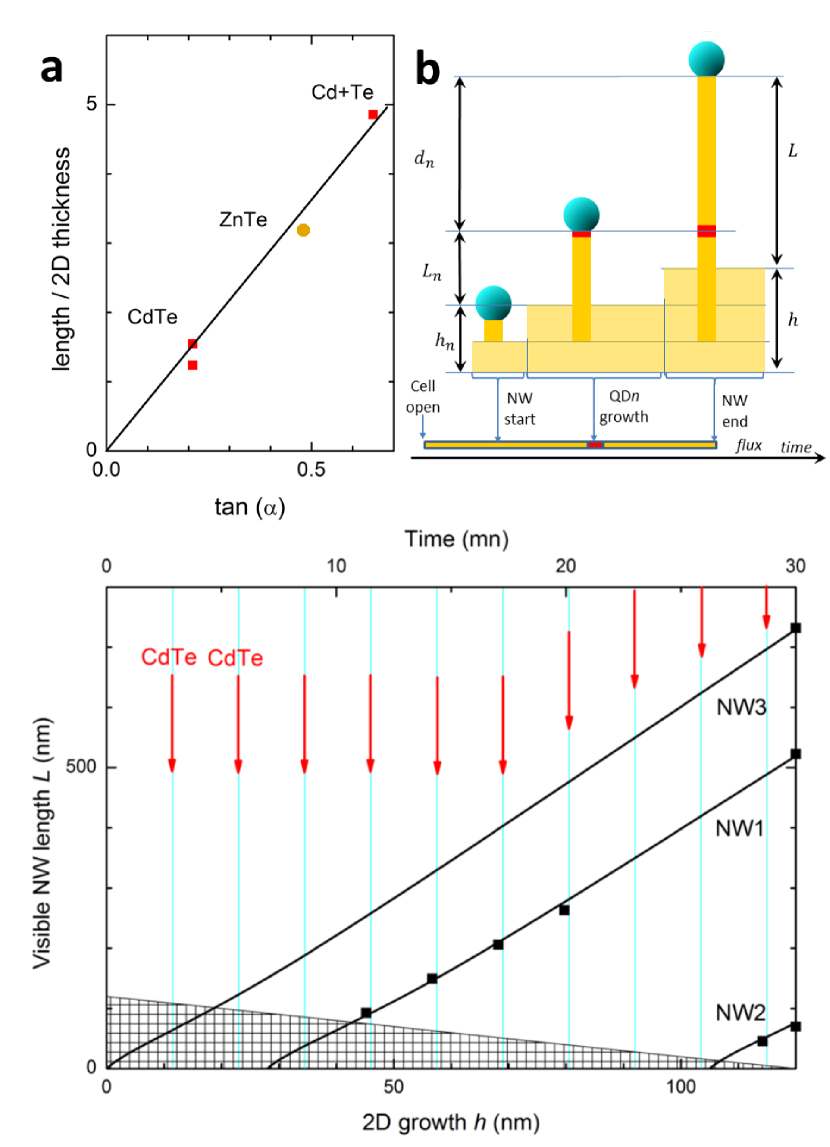
The visible length of the nanowire, , the radius of the NW, the radius of the gold nanoparticle, and the radius of the gold-tip contact are available from the HAADF images in Fig. 2 (see also Fig. 4); the distance of several CdTe insertions from the tip, , are measured on the GPA images. Figure 3b describes the growth of a NW with a CdTe insertion, with the characteristic lengths involved. The length is the visible length of the NW, a part of the NW being hidden by the parasitic growth of the 2D layer. The visible length at the moment of the growth of the CdTe insertion is obtained as , where the total thickness of the parasitic 2D layer, nm, was measured on a cleavage plane, and its thickness at the moment of the growth of the CdTe insertion, , is deduced from the growth sequence.
Fig. 3c plots and for the two NWs of Fig. 2. Even without the lines which show the fit described in section III below, it appears that the NWs started to grow after a significant incubation time. This will be addressed more quantitatively in the remainder of the paper, and possible reasons will be discussed in Section IV. Note that the existence of this incubation time was confirmed by exposing a series of samples, prepared under the same conditions, to the Zn+Te flux for 2, 10 or 30 min.: the number of nanoparticles having catalyzed the growth of NWs was found to increase. Full details are given in Ref.RuedaPhD, .
II.2.2 Gold particle
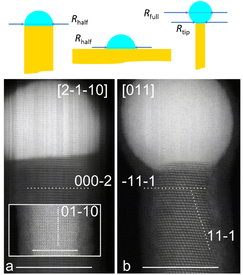
Figure 4a shows the gold catalyst on a NW with the wurtzite crystal structure. The NW was long enough that it vibrates under the electron beam near the tip, so that only (0002) planes are visible in the NW; yet the wurtzite structure was clearly observed closer to the NW base, as shown in the inset of Fig. 4a. The NW exhibits a flat tip, and the shape of the gold particle is close to a half sphere with a diameter matching the NW diameter. This is close to the shape assumed by the gold particles sitting at the surface of the buffer layer before opening the shutter to start the growth of the NWs.RuedaDewett ; RuedaPhD This configuration is well known for III-V NWs with the wurtzite structure, and it is associated to a nucleation at the edge of the facet forming the top of the NW.Krogstrup An extensive, statistically significant study of the interface is however out of the scope of the present paper.
All tapered nanowires which have been observed by TEM have the zinc-blende structure. Long tapered NWs show a gold particle with a shape closer to a full sphere, as shown in Fig. 4b. This is expected if the nucleation takes place on an inclined facet. Wen Indeed, the interface is far from being flat, and a meniscus (or incompletely formed facet) is clearly apparent. Hemispherical gold nanoparticles are also observed by SEM at the tip of tapered NWs, particularly at the tip of the shorter ones. Note that a change of shape - and of facet morphology - has been observed on III-V NWs, and may even take place regularly during the growth of the NW. Wen In addition, several facets (3 in the simplest case) may form, not necessarily at the same time. For such full-sphere nanoparticles, three characteristic diameters may be considered: the measured diameter of the full sphere, , the diameter of the initial particle which is approximately half-sphere,RuedaDewett ; RuedaPhD , and the diameter of the contact area between the particle and the NW tip, . If the shape change from half sphere to full sphere takes place at constant volume, the droplet diameter is slightly reduced, from to , i.e., by 25%. More significant is the fact that the diameter at the interface between the gold particle and the NW - the contact diameter - is definitely smaller. It is this diameter which defines the diameter of the growing NW (hence the lateral size of a quantum dot embedded in the NW, but also partly the growth rate, as recalled later on). Typical values of the diameter of the gold particle are 20 nm. The diameter of the NW neck below the spherical gold particle is more difficult to measure; typical values measured by SEM are around 15-20 nm but this includes an amorphous or ill-crystallized surface layer, which is due either to some oxidation of the NW, or to post-growth deposition; the crystalline core imaged by TEM is thinner, 6 to 10 nm (see Fig 4, and also Fig. 5 of Ref. Rueda2014, ); such a value fairly matches the diameter of CdTe dots imaged by EDX in Ref. RuedaEDX, .
II.2.3 The role of the gold particle shape and size
With the previous samples, we have explored the growth at a temperature (C) where the distribution of gold nanoparticles is relatively narrow. Figure 5a shows a SEM image of a sample obtained by first dewetting the gold nanoparticles at 350∘C, and rapidly increasing the temperature to 375∘C to start the growth with an additional Te flux. It displays cylinder-shaped NWs (blue arrows), and cone-shaped NWs (green arrows) - quite similar to samples grown under stoichiometric conditions at C. This indicates that the increase of the sample temperature and the presence of a higher Te flux compensate each other, a hint that the evaporation of Te atoms is probably the limiting mechanism. Also visible are aborted or badly formed NWs (yellow arrows) and thick, inclined NWs (bottom right corner).
Fig. 5b plots the volume of the gold nanoparticle, vs the NW length. As observed previously in Fig. 4, the nanoparticles assume two different shapes (close to half-sphere and close to full sphere), which are identified in Fig. 5 by different symbols. Again one observes a stronger dispersion in the NW length for the cone-shaped NWs than for the cylinder-shaped ones. But also one observes (1) a significant dispersion in the nanoparticle size, which is due to an evolution of the nanoparticles during the ramp to the higher growth temperature, and (2) a correlation between the shape of the gold particle at the tip (half-sphere or full-sphere) and the length of the cone-shaped NWs: the two sets of NWs occupy two different areas, delineated by the grey lines.
As a result of the dispersion in the nanoparticle size, the trend between the base diameter and the NW length (Fig. 5c) appears as partially blurred when compared to Fig. 1. To cope with this dispersion, in Fig. 5d we plot the ratio of the base diameter to the size of the gold nanoparticle, where is the radius of the half-sphere with the same volume (see Fig. 5b). This plot will be used in the following section, in the frame of a growth mechanism taking into account the diffusion of adatoms and the incubation time mentioned previously, but also the effect of the nanoparticle size and shape: the results of this model are summarized by the lines in Fig. 5d,e, to be discussed in section III.
III Diffusion-limited model
The growth of nanowires is strongly influenced by two parameters: the nucleation at the Au catalyst particle, and the diffusion of species on the surfaces. On one hand, complex models based on growth kinetics, involving the interaction of atoms in various thermodynamic states at the Au-NW interface, have been proposed for the VLS growth of III-V NWs.Glas2010 These models rely on transition state kinetics driven by the minimization of the free energy of the total system. On the other hand, diffusion-dependent nanowire growth models have also been developed .Dubrovskii2006 In these type of models, the morphology (length and shape) of the nanowires is directly related to different values of the diffusion length on the substrate and along the NW sidewalls. These models are also known to apply to a wide range of growth conditions of III-V and Si NWsDubrovskii2009 and even to CdTe NWs.Dubrovskii2012
In this section we focus on the role of adatom diffusion on the growth of ZnTe NWs by MBE at low temperature: any possible effect of the nucleation at the gold particle / NW tip is ignored. We obtain analytical expressions which we can readily exploit to extract quantitative parameters (diffusion lengths, incubation times) from the plots in Fig. 1, 3, 5.
III.1 Axial and lateral growth rates in the diffusion-limited model
The description is made simpler if we keep in mind that:
-
•
The density of Au droplets (and even more the density of NWs) on the substrate is low enough that we can consider a single, isolated NW.
-
•
The NW is perpendicular to the substrate surface.
-
•
The temperature is low enough that re-evaporation is negligible: the diffusion length is defined by the incorporation of adatoms on the substrate or on the NW facets.
-
•
We observe a NW growth rate significantly larger than that of the 2D layer; hence we calculate only the contribution of adatoms diffusing from the substrate and the NW sidewalls to the gold particle. Indeed, the contribution of the direct flux onto the Au droplet is not too different from the contribution to the 2D layer away from the NW (they are equal for a half-sphere droplet and complete sticking); hence the length we calculate is close to the length visible above the 2D layer.
The diffusion-based NW growth model adapted to these conditions is described in Appendix A. It involves the general solution of the diffusion equations of adatoms on the NW sidewalls in 1D, and on the substrate surface in 2D with a circular symmetry. It assumes complete trapping at the tip of the NW (catalyst acting as a perfect sink).Dubrovskii2006 It results in simple analytical relationships between the length of the NW (axial growth) and the thickness of the 2D layer far from the NW (growth in the absence of catalyst), on one hand, and between and the radius at the NW basis (lateral growth), on the other hand. These relationships are derived from Eq. 8 and A in Appendix A where we set all sticking coefficients to unity (this is a reasonable approximation for the ZnTe surfaces at C):
| (1) |
and
| (2) |
where and are the diffusion length on the substrate and along the NW sidewalls, respectively, is the radius of the contact area between the gold catalyst and the NW tip, is the initial radius of the gold nanoparticle. We have replaced the ratio of lateral to substrate flux by its value, , and we have defined an effective diffusion length , which is small with respect to and kept constant in the calculation, as discussed in Appendix A.
Examples of Eq. 1 are displayed in Fig. A2a: the initial growth rate (for ) is governed by the diffusion on the substrate; for most of the NWs described here, the final length so that the growth rate during most of the growth is the asymptotic growth rate due to the lateral flux, given by .
The lateral growth at the basis of the NW (Eq. III.1) reflects the fact that the adatom density on the sidewalls at the basis of the NW is linked to the adatom density on the substrate, so that the difference in the incorporation rates leads to . Figure A2b shows that this holds for most of the growth, with a small correction due to the lateral flux, and except for the initial step where both the NW length and the lateral growth are small. We will use Eq. III.1 in the analysis of experimental data, but the asymptotic form suggests that the diameter of the NW at its basis is a rather good measure of the time between the actual start of the NW growth and its end.
III.2 The model applied to experimental data
III.2.1 The markers technique
The most complete data are those obtained on single NWs with CdTe insertions, Fig. 3. A reasonable fit (black solid lines) is obtained with the same values of the diffusion lengths for both NWs (=18 nm and =78 nm), assuming that the growth of the NW does not start immediately after the opening of the cell. A further criterion for the fit (not shown) is that the measured and calculated values of the base diameter coincide. The shape of the gold particle at the tip of NW1 and NW2 is close to a full sphere: the fit in Fig. 3 assumes that the nanoparticles turned very rapidly to a full-sphere; hence in Eq. A the initial diameter, , and the contact diameter during the growth, , are both taken equal to . Moreover, we have assigned to the diameter of the crystalline core of the NWs measured by TEM, nm for NW1 and 7.9 nm for NW2. The length measured for NW3 is well fitted assuming the same values of diffusion lengths, and nm. Actually, there is a 2.5 nm thick amorphous layer around the NW, which can be due to the oxidation of the NW or to a post-growth deposition. If we take the external diameter instead of that of the crystalline core in Eq. A, an as-good fit is obtained with unchanged and increased by 15 to 20% (not shown).
The main conclusion here is that the broad range of length values observed involves a significant incubation time: the 2D layer thickness was already 30 nm when NW1 started, and 100 nm for NW2. This delayed growth is the main reason for the length dispersion of the 3 NWs shown in Fig. 3.
It will be further confirmed now using a complementary approach: indeed a similar information can be deduced from the observation of an ensemble of NWs (without markers) and the statistics on the length / base diameter relationship.
III.2.2 Axial vs. radial growth
We start with the results shown in Fig. 5. Keeping in mind the two possible shapes of the gold nanoparticle, close to half-sphere or close to full sphere, we may expect three typical behaviors: NWs driven by a nanoparticle staying half-sphere up to the end of growth (case 1 below), NWs driven by a nanoparticle turning to full sphere from the beginning (case 2), and nanoparticle turning from half-sphere to full sphere shortly after the growth start (case 3). As the growth rate is expected to increase as the contact diameter decreases, the full-sphere-NWs are expected to grow faster than the half-sphere-NWs in spite of a larger nanoparticle volume: the relevant diameter is 6 to 8 nm in the first case, against 15 to 18 nm in the second case.
-
•
(1) One clearly identifies in Fig. 5d a series of half-sphere NWs with a large base diameter and small length, which we tentatively ascribe to the extreme case of full-time half-sphere NWs. Assuming in Eq. A, with the additional assumption that the longest NW of the series started to grow immediately, a reasonable fit is obtained as shown by the solid line, with =38 nm and =126 nm. The different values of the NW length, from the shortest to the longest, correspond to (i) increasing values of the growth duration, with the shortest NW starting on a 2D layer of thickness nm (40 nm still to go) up to the full nm for the longest one (immediate start), (ii) a decreasing nanoparticle size measured within this series of half-sphere NWs (green crosses in Fig. 5e). Taking both effects into account, and using a purely heuristic dependence between the contact area and the final length (dashed line in Fig. 5e), we obtain the green solid line in Fig. 5e.
-
•
(2) For the opposite extreme, the case of a full sphere since the beginning, we keep the same values of the diffusion lengths and decrease the value of to 7.3 nm to obtain the largest length observed: we then obtain the lowest red dashed line in Fig. 5d; note that the previous dashed and solid lines in Fig. 5e satisfactorily account for this experimental point.
- •
Intermediate data - in particular half-sphere data below the full line, or full-sphere data between the two dashed lines - can be ascribed to NWs with a non-circular shape of the nanoparticle, or a shape which evolves during the growth. Finally, the green solid line in Fig. 5e separates the half-sphere NWs from the full-sphere NWs, it also constitutes a good average fit of the base-diameter / length dependence.
A good overall fit is also obtained using the same procedure for the other sets of data. For instance, in Fig. 1, we had to assume a diameter decreasing from =20nm to =6 nm, and diffusion lengths =78 nm and =23 nm, close to those of the sample in Fig. 3, as expected since the growth conditions are the same (the slight difference is at least partly explained that we used diameter values obtained either for the crystalline core observed by TEM or the overall NW imaged by SEM). For a sample grown under Te excess (not shownRuedaPhD ), slightly lower values of the diffusion lengths, =57 nm and =18 nm, are obtained, assuming a similar distribution of the gold nanoparticle size. All values are gathered in Table I below.
IV Discussion and conclusion
In summary, the large dispersion in the length of the zinc-blende ZnTe NWs is ascribed to the presence of two steps in the growth catalyzed by gold nanoparticles, which initially feature a half-sphere shape: the start of the NW growth, and the evolution of shape of the gold nanoparticle from half-sphere to almost full sphere. The longest NWs have started immediately with a nanoparticle rapidly turning to full-sphere, hence a small contact radius, with facets or a meniscus at the interface. The shortest NWs started with a delay and with a nanoparticle staying with a half-sphere shape on top of the 2D layer and the NW tip. Some nanoparticles never give rise to a NW or even are buried into the 2D layer. The direct effect of the particle size on the growth rate exists but it is mostly hidden by the existence of the incubation delay.
Within this scheme, the characteristics of the NWs are well accounted for using a simple diffusion-limited model, with two diffusion lengths, on the NW sidewalls and on the substrate. Table 1 shows the values used to fit our data: the decrease induced by adding a Te flux suggests that the limiting process under these conditions is the diffusion of Zn (the diffusion length of Zn is reduced if the density of Te adatoms increases). Increasing the temperature increases the diffusion length under Te excess, presumably due to an activation of Te desorption.
| Growth | (nm) | (nm) | Fig. |
|---|---|---|---|
| C-stoichio | 78 | 18 | 2, 3 |
| C-stoichio | 78 | 23 | 1 |
| C-Te | 57 | 18 | Ref. RuedaPhD, |
| C-Te | 126 | 38 | 5 |
With such values of the diffusion length on the NW sidewalls, the growth rate at the tip of a NW with a length of several 100 nm is mainly due to the lateral flux, , and . This is important as it determines the length of a quantum dot inserted in the NW, but also its composition if the material is an alloy, for instance a diluted magnetic semiconductor. The diameter of the quantum dot is determined by the contact diameter ().
Our uncertainty on the value of (crystalline core or the whole NW including the amorphous shell), and that on the value of , have a straightforward impact on the value of . In addition, sticking coefficients lower than unity will change the value of , by a factor (see Eq. A).
The value of , the diffusion length on the substrate, is mainly deduced from the measure of the lateral growth at the basis of the NW. Figure A2 suggests that for the present values of the parameters, both the effect of the depletion of adatoms around the NW basis and the contribution of the lateral flux are small, and moreover they partially compensate each other. Here again, sticking coefficients lower than unity will affect the absolute value of , as we actually determine . Note that our values of are quite small, but they are of the same order as the size of the structures observed at the bottom of the NWs: a crater or a zone with no growth in the case of zinc-blende NWs, signaling a transfer of material from the substrate to the NW, and a pyramid progressively formed at the bottom of wurtzite NWs, as the signature of a transfer from the NW to the substrate.
We have noted that the effect of the additional Te flux and of the growth temperature (Table 1) suggests that it is the diffusion of Zn which limits the growth rate - even if a role of Te diffusion is not totally ruled out. The growth of ZnTe NWs thus strongly differs from the growth of self-assembled GaAs NWs, which is characterized by a strong diffusion of Ga towards the tip, and a growth rate determined by the As4 flux to the Ga droplet Colombo , either directly from the effusion cell, or by desorption Ramdani . In our case, we observe the opposite behavior, that adding a Te flux decreases the axial growth rate by decreasing .
An important result of the present study is the evidence of an incubation time between the onset of the molecular beam and the start of the NW growth. Different systems have been shown previously to exhibit significant incubation times. One reason may be the formation of the proper catalyst/semiconductor interface. When GaAs NWs are grown by gold-catalyzed MBE on a silicon substrate under vapor-liquid-solid conditions,Breuer an initial step is observed where ”traces” creep on the Si surface until they meet a GaAs nucleus. This is interpreted as due to a large difference in the interface energy on the Si substrate and on the GaAs nucleus. We do observe such traces (yellow arrows in Fig. 1 and 5), but in our case the gold nanoparticles are formed on a ZnTe buffer layer. For other preparation and growth conditions, the incubation is attributed to the formation of a pinhole in the Si oxide, and the formation of the Ga droplet Fontcuberta ; Rudolph . Another contribution may be brought by the existence of a threshold in the composition of the catalyst droplet. In the case of Si NWs on Si substrates, depending on the growth conditions, this threshold has been discussed in terms of supersaturation of the gold droplet, Dhalluin or in terms of diffusion within the solid catalyst to achieve its fusion (transition from vapor-solid-solid, VSS, to vapor-liquid-solid, VLS conditions).Kalache Such a transition from VLS to non-VLS conditions was observed to depend on the As/Ga ratio for GaAs NWs on Si.Rudolph In all cases the incubation time is expected to increase with the catalyst size, which is indeed a trend which is suggested by the catalyst size dependence on final NW length (data in Fig. 5, and the heuristic dependence used in the overall fits). A dispersion in the value of the diffusion length on the substrate may enhance the dispersion in the incubation times. A specific study is needed to disentangle and evaluate the possible contributions, in order to obtain a reasonably narrow length distribution.
Finally, we may come back to the NW of Fig. 2b. From quantitative profiles (not shown), the gold nanoparticle diameter is 35 nm, the NW diameter below the gold nanoparticle is 26 nm (total) and 20-22 nm (not counting the oxide shell), the NW diameter at the base is 55 nm (with the oxide) and 40 nm (without the oxide). 8 CdTe insertions are detected along the length of 550 nm, regularly spaced with a period nm. The size of the gold nanoparticle is clearly larger than average, and such that we expect it to remain as a 3D object, or to give rise to an inclined NW (see an example with the black arrow in the inset of Fig. 1). In this case a larger contact area and a stronger lateral flux due to the inclined configuration tend to increase the tapering. Note also that the lateral growth of ZnTe on the side of the CdTe insertion is not symmetrical, as evidenced by the off-axis position of the CdTe insertions at the bottom of the NW.
To conclude, we have demonstrated two approaches to unravel the characteristics of the MBE growth of NWs at low temperature, with the help of analytical results from an adapted diffusion-based model. Applied to the growth of ZnTe NWs, the main results are:
-
•
the existence of an incubation time before the actual start of the NW, which remains to be understood, and if possible suppressed;
-
•
except for very short NWs, the central role of lateral flux in determining the axial growth rate (hence the length and composition of an embedded quantum dot); note that the incubation time does not affect this phase of the growth;
-
•
the formation of a narrow contact area, which determines the diameter of the quantum dotRuedaEDX but also contributes to determine the axial growth rate;
-
•
the possibility of lateral growth without changing the growth temperature, allowing us to fabricate core-shell structures with good interfaces or tapered NWs; at the basis of the NW, the lateral growth is governed by the diffusion of substrate adatoms; higher along the NW, the role of the lateral flux progressively increases.
Appendix A Calculation
Or goal here is not to derive a general theory of NW growth, but to obtain a simple model, adapted to the present case, with analytical results, likely to serve as a guide for future studies.
We consider a low density of NWs, perpendicular to the substrate. A diffusion-based NW growth model is built from the general solution of the diffusion equations of adatoms on the NW sidewalls in 1D, and on the substrate surface in 2D with a circular symmetry. The flux impinging onto the substrate (actually, the ZnTe buffer layer) far from the NW induces the presence of adatoms with a density , where is the residence time of an adatom which diffuses on the surface over a length before incorporation (or desorption). We define similarly a uniform-limit adatom density on the NW sidewalls, , with the residence time and the diffusion length. For the sake of simplicity, we keep the same diffusion constant . The ratio of adatom densities is thus (with incidence angle, i.e., the angle between the cell axis and the substrate normal)
| (3) |
The local densities of adatoms (number of adatoms by surface unit), on the substrate, and on the NW sidewalls, are solutions to the diffusion equations and can be written as follows:
| (4) |
where is the radial coordinate centered on the NW axis and increasing when moving away from the NW, and is the coordinate along the NW axis, perpendicular to the substrate and increasing towards the tip of the NW. and are modified Bessel functions.
The four coefficients , , , , are to be determined by boundary conditions. We take the simplest ones:
-
•
For a weak density of NWs, hence .
-
•
The hopping probabilities of adatoms, from the NW to substrate and from the substrate to the NW, are assumed to be symmetric: , where is the nanowire radius at the base.
-
•
The adatom current at the vicinity of the NW-substrate interface are in equilibrium (conservation of the adatom currents):
-
•
Complete trapping at the tip of the NW (catalyst droplet acting as perfect sink): , where is the height of the nanowire. This last condition is valid for a purely diffusion-driven model .Dubrovskii2006 In the more complex case of kinetic-driven growth Glas2010 (not treated here), where the thermodynamical mechanisms in the catalyst droplet limiting the axial growth need to be taken into account, this condition is modified to a condition on .
These boundary conditions allow us to determine the constants in equations A and to obtain the following expression for the NW adatom density:
| (5) |
with and
Here we have defined an effective diffusion length , and we have assumed that . Note that if the diffusion equation in the substrate was in 1D instead of in 2D, would simply be . In 2D, depends on , hence its value changes as growth proceeds. Indeed, when we calculate the values of for from 10 to 35 nm (the range of NW base radius values found for our ZnTe NWs, see Fig. 1), we find to , and for typical values of (see below), remains of the order of a few 10 nm. In addition, influences mainly the NW growth when they are short (i. e. when the effect of lateral growth is still negligible). When the NWs are longer, it is that dominates the growth, hence the variations of are masked by the larger values of . In the following, we take constant and small with respect to .
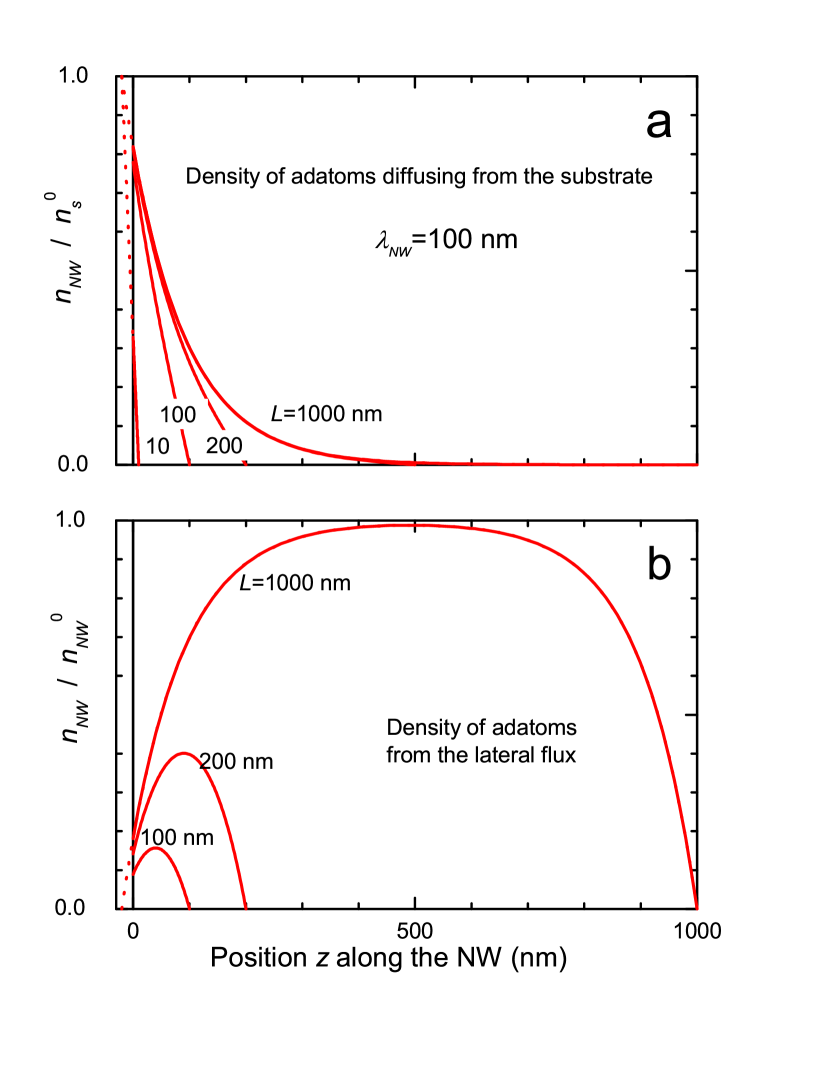
The two contributions to Eq. 5, from the flux arriving to the substrate, and from the flux arriving laterally, are plotted in Fig. A1 for typical values nm, nm and nm. Note that all curves converge at as shown by the dotted lines, which identifies as an effective diffusion length on the substrate, as seen from the NW.
The growth rates for the NW length (axial growth), for the NW radius at the base (lateral growth) and for the 2D pseudo-substrate with height are given by:
| (6) |
In these equations, is the volume occupied by an atom in the crystal; , and are the incorporation rate at the substrate, at the NW facets and at the tip of the NW (at the interface with the Au catalyst particle); is the growth speed on the substrate (at the end of the growth, the final thickness of this re-grown layer is ).
From Eq. A and Fig. A1a, we conclude that the contribution to the growth from adatoms diffusing from the substrate is: i) important for short NWs, , with a linear decrease of with , and ii) weak for long NWs, , with a exponential decrease of with .
Figure A1b shows that the contribution to the growth from the lateral flux is proportional to for short NWs. For long NWs, the adatoms arriving at the middle part of the NW are incorporated locally (with the formation of a plateau) and the contribution to the NW axial growth is proportional to .
| (7) |
With the simplifying assumption that is constant, Eq. 7 can be integrated, giving the nanowire length as a function of the thickness of the re-grown layer:
| (8) |
This dependence of on is plotted in Fig. A2a for different contributions from the substrate (different values of ).
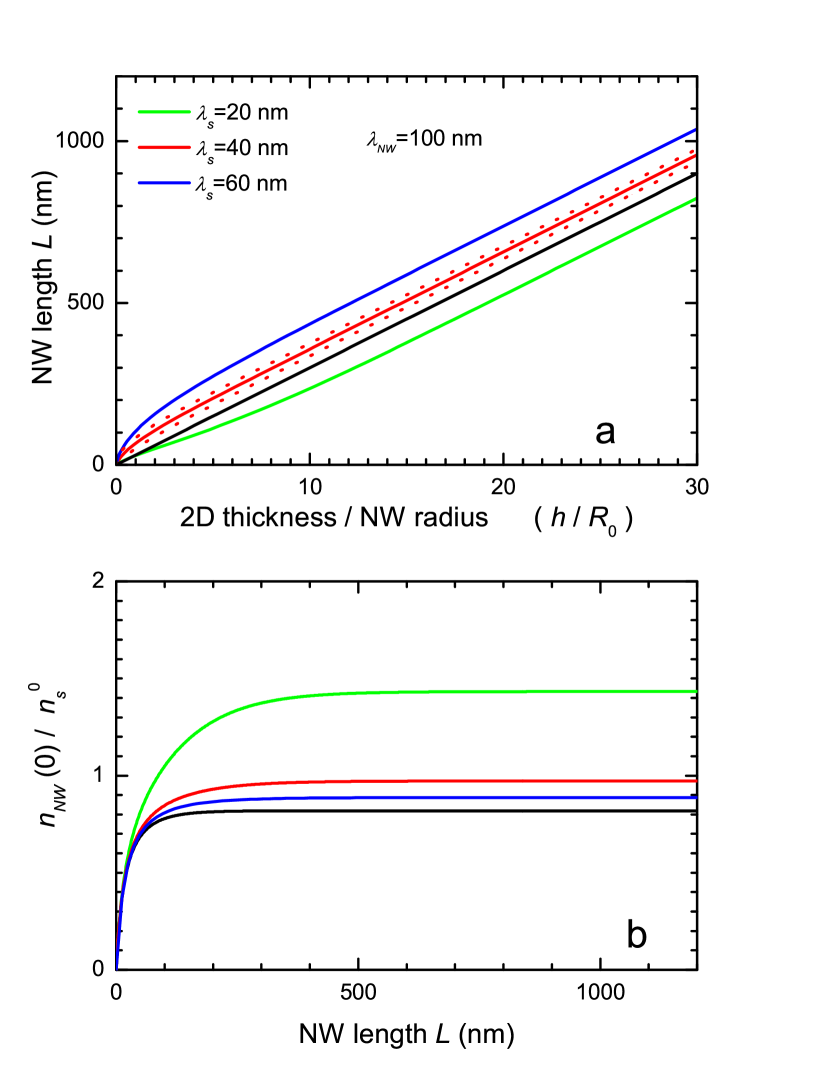
For the long NWs , the contribution to the NW axial growth from the adatoms arriving to the substrate and diffusing up the NW walls up to the catalyst droplets is negligible. The dominant contribution to the axial growth is that from the lateral flux, with a constant growth rate (dashed black line). A change of the values of to 10 nm and to 50 nm (extreme values observed in our samples) makes only minor changes of (red dotted lines), which validates the hypothesis of a constant value.
Hence, the contribution from the substrate influences the axial growth rate of the NWs only at the early stages of growth. For short NWs (), it determines how fast the NW starts to grow: the growth speed at nm is lower than the final slope while at nm it is larger.
The lateral growth rate at the NW base (), in the case where , is given by:
| (9) | |||||
| where | |||||
In Fig. A2b we plot the value of , for different contributions from the substrate (different values of ). We observe that for short NWs, the lateral growth is slow and that the lateral flux does not influence the growth (the four lines are merged together). For long NWs, the contribution from the lateral flux remains relatively weak, and the lateral growth rate is constant with , as a result of . Thus, the lateral growth at the NW base is a good measure of the NW growth time, which can be interesting in samples where the NWs start to grow at different times.
Finally, the variation of the NW radius at the base, , with the NW length can also be determined:
| (10) |
which can be integrated to obtain . If , a good approximation is to ignore the second term in the numerator, so that
| (11) |
Here we made a simplified distinction between the contact radius during the main part of the growth, and its initial value at the beginning of the NW growth.
Acknowledgements.
This work was performed in the joint CNRS-CEA group ”Nanophysique & semiconducteurs”, and in the frame of the French National Agency project ”Magwires” (ANR-11-BS10-013). We thank all the members of the Magwires project for many discussions. We also acknowledge a grant from the Laboratoire d’excellence LANEF in Grenoble (ANR-10-LABX-51-01).References
- (1) M. V. Nazarenko, N. V. Sibirev, Kar Wei Ng, Fan Ren, Wai Son Ko, V. G. Dubrovskii, and C. Chang-Hasnain, J. Appl. Phys. 113, 104311 (2013).
- (2) H. J. Joyce, P. Parkinson, Nian Jiang, C. J. Docherty, Qiang Gao, H. Hoe Tan, C. Jagadish, L. M. Herz, and M. B. Johnston, Nano Lett. 14, 5989 (2014).
- (3) O.Demichel, M. Heiss, J. Bleuse, H. Mariette and A. Fontcuberta i Morral, Appl. Phys. Lett. 97, 201907 (2010).
- (4) Niels Gregersen, Torben R. Nielsen, Julien Claudon, Jean-Michel Gérard, and Jesper Mørk, Optics Letters 33, 1693 (2008).
- (5) Y. M. Niquet, C. Delerue and C. Krzeminski, Nano Lett. 12, 3545 (2012).
- (6) F. Boxberg, N. Søndergaard, and H.Q. Xu, Nano Lett. 10, 1108 (2010).
- (7) D. Ferrand and J. Cibert, Eur. Phys. J. Appl. Phys. 67, 30403 (2014).
- (8) Q. F. Meng, C. B. Jiang and S. X. Mao, Appl. Phys. Lett., 94, 043111 (2009).
- (9) S. Bounouar, M. Elouneg-Jamroz, M. den Hertog, C. Morchutt, E. Bellet-Amalric, R. André, C. Bougerol, Y. Genuist, J.-P. Poizat, S. Tatarenko, and K. Kheng, Nano Lett. 12, 2977 (2012).
- (10) Z. Fan, D. J. Ruebusch, A. A. Rathore, R. Kapadia, O. Ergen, P. W. Leu, and A. Javey, Nano. Research 2, 829 (2009).
- (11) P. Wojnar, E. Janik, L. T. Baczewski, S. Kret, E. Dynowska, T. Wojciechowski, J. Suffczynski, J. Papierska, P. Kossacki, G. Karczewski, J. Kossut, and T. Wojtowicz, Nano Lett. 12, 3404 (2012).
- (12) A. Artioli, P. Rueda-Fonseca, P. Stepanov, E. Bellet-Amalric, M. den Hertog, C. Bougerol, Y. Genuist, F. Donatini, R. André, G. Nogues, K. Kheng, S. Tatarenko, D. Ferrand, and J. Cibert, Appl. Phys. Lett. 103, 222106 (2013).
- (13) M. Szymura, P. Wojnar, L. Klopotowski, J. Suffczynski, M. Goryca, T. Smolenski, P. Kossacki, W. Zaleszczyk, T. Wojciechowski, G. Karczewski, T. Wojtowicz, and J. Kossut, Nano Lett. 15, 1972 (2015).
- (14) A. Artioli, P. Rueda-Fonseca, M. Orrù, T. Cremel, S. Klembt, K. Kheng, F. Donatini, E. Bellet-Amalric, M. Den Hertog, C. Bougerol, J.-F. Motte, Y. Genuist, M. Richard, R. André, E. Robin, S. Tatarenko, J. Cibert and D. Ferrand, 17th International Conference on II-VI compounds and related materials, Paris, 13-18 September 2015.
- (15) M. Jeannin, A. Artioli, P. Rueda-Fonseca, M. Orrù, M. Den Hertog, M. Lopez-Haro, Y. Genuist, R. André, E. Robin, S. Tatarenko, E. Bellet-Amalric, J. Cibert, D. Ferrand, and G. Nogues, Nanowires Workshop - 2015, Barcelona, Catalonia, Spain, October 26-30th, 2015.
- (16) P. Rueda-Fonseca, E. Bellet-Amalric, R. Vigliaturo, M. Den Hertog, Y. Genuist, R. André, E. Robin, A. Artioli, P. Stepanov, D. Ferrand, K. Kheng, S. Tatarenko, and J. Cibert, Nano Lett. 14, 1877 (2014).
- (17) K. Yang and L. J. Schowalter, Appl. Phys. Lett. 60, 1852 (1952).
- (18) P. Rueda-Fonseca et al., unpublished.
- (19) Rueda-Fonseca, P. Magnetic quantum dots in II-VI semiconductor nanowires PhD thesis 2015, Université de Grenoble, available at https://hal.archives-ouvertes.fr/hal-01167875v1.
- (20) P. Rueda-Fonseca, E. Robin, E. Bellet-Amalric, M. Lopez-Haro, M. Den Hertog, Y. Genuist, R. André, A. Artioli, S. Tatarenko, D. Ferrand, and J. Cibert, Nano Lett. 16, 1637 (2016).
- (21) M.I. den Hertog, H. Schmid, D. Cooper, J.L. Rouvière, M.T. Björk, H. Riel, P. Rivallin, S. Karg and W. Riess. Nano Lett. 9, 3837 (2009).
- (22) M. Hÿtch, E. Snoeck and R. Kilaas, Ultramicroscopy 74, 131 (1998).
- (23) J.-L. Rouvière and E. Sarigiannidou, Ultramicroscopy 106, 1 (2005).
- (24) J.-C. Harmand, F. Glas, and G. Patriarche, Phys. Rev. B 81, 235436 (2010).
- (25) F. Glas, J.-C. Harmand, and G. Patriarche, Phys. Rev. Lett. 104, 135501 (2010).
- (26) P. Krogstrup, S. Curiotto, E. Johnson, M. Aagesen, J. Nygȯrd, and D. Chatain, Phys. Rev. Lett. 106, 125505 (2011).
- (27) C.-Y. Wen, J. Tersoff, K. Hillerich, M. C. Reuter, J. H. Park, S. Kodambaka, E. A. Stach, and F. M. Ross, Phys. Rev. Lett. 107, 025503 (2011).
- (28) F. Glas, J. Appl. Phys. 108, 073506 (2010).
- (29) V. G. Dubrovskii, N. V. Sibirev, R. A. Suris, G. . Cirlin and V. M. Ustinov, M. Tchernysheva and J. C. Harmand, Semiconductors 40, 1075 (2006).
- (30) V. G. Dubrovskii, N. V. Sibirev, G. E. Cirlin, I. P. Soshnikov, W. H. Chen, R. Larde, E. Cadel, P. Pareige, T. Xu, B. Grandidier, J.-P. Nys, D. Stievenard, M. Moewe, L. C. Chuang, and C. Chang-Hasnain, Phys. Rev. B 79, 205316 (2009).
- (31) V. G. Dubrovskii, A. D. Bolshakov, B. L. Williams, and K. Durose, Nanotechnology 23, 485607 (2012).
- (32) C. Colombo, D. Spirkoska, M. Frimmer, G. Abstreiter, and A. Fontcuberta i Morral, Phys. Rev. B 77, 155326 (2008).
- (33) M. R. Ramdani, J.-C. Harmand, F. Glas, G. Patriarche, and L. Travers, Cryst. Growth Des. 13, 91 (2013).
- (34) S. Breuer, M. Hilse, A. Trampert, L. Geelhaar, and H. Riechert, Phys. Rev. B 82, 075406 (2010).
- (35) Appl. A. Fontcuberta i Morral, C. Colombo, G. Abstreiter, J. Arbiol, and J. R. Morante Appl. Phys. Lett. 92, 063112 (2008).
- (36) D. Rudolph, S. Hertenberger, S. Bolte, W. Paosangthong, D. Spirkoska, M. Döblinger, M. Bichler, J. J. Finley, G. Abstreiter, and G. Koblmüller, Nano Lett. 11, 3848 (2011).
- (37) F. Dhalluin, T. Baron, P. Ferret, B. Salem, P. Gentile, and J.-C. Harmand, Appl. Phys. Lett. 96, 133109 (2010).
- (38) B. Kalache, P. Roca i Cabarrocas, and A. Fontcuberta i Moral, Jap. J. Appl. Phys. 45, L190 (2006). ——————