Shaping, imaging and controlling plasmonic interference fields at buried interfaces
Abstract
Filming and controlling plasmons at buried interfaces with nanometer (nm) and femtosecond (fs) resolution has yet to be achieved and is critical for next generation plasmonic/electronic devices. In this work, we use light to excite and shape a plasmonic interference pattern at a buried metal-dielectric interface in a nanostructured thin film. Plasmons are launched from a photoexcited array of nanocavities and their propagation is filmed via photon-induced near-field electron microscopy (PINEM). The resulting movie directly captures the plasmon dynamics, allowing quantification of their group velocity at 0.3c, consistent with our theoretical predictions. Furthermore, we show that the light polarization and nanocavity design can be tailored to shape transient plasmonic gratings at the nanoscale. These results, demonstrating dynamical imaging with PINEM, pave the way for the fs/nm visualization and control of plasmonic fields in advanced heterostructures based on novel 2D materials such as graphene, \ceMoS2, and ultrathin metal films.
I Introduction
Surface plasmon polaritons (SPPs)maier07 are considered ideal for circuitry miniaturization to nanoscale dimensionsbarnes03 , due to their inherent surface-bound and spatial confinement characteristics. This makes them appealing for various applications, such as nanoscopic signal processingozbay06 and high resolution sensingstewart08 . However, considering the fs temporal and nm spatial scales involved, direct real space characterization of evanescent waves presents a significant experimental challenge, especially in materials and devices involving buried interfaces and complex heterostructures.
Several optics-based approaches have been developed to meet the challenge of tracking surface-bound SPPs with appropriate resolution, notably dual-color coherent anti-Stokes Raman scattering (CARS)liu12 and scanning tip based techniques such as near-field scanning optical microscopy (NSOM) bohm94 ; gersen05 . In recent years, the spatial and temporal resolution limits of these optical techniques have been pushed to the 10s of nm and 100s of fs wagner14 ; nishiyama15_2 . In an alternative approach, the use of electron photoemission for detection, as in time-resolved nonlinear photoemission electron microscopy (TR PEEM)petek97 ; kubo05 ; kubo07 , has allowed for comparable spatial resolution in imaging SPPs, with time resolution extending down to the few-fs single optical cycle regime. Recent advances in TR-PEEM methods have facilitated the successful spatiotemporal mapping of localized and propagating surface plasmons in a variety of systemsaeschlimann10 ; lemke13 ; lemke14 ; gong15 ; marsell15 . However, as TR-PEEM relies on sample-emitted photoelectrons, and scanning-tip-based techniques require physical probe proximity to the evanescent field, both are inherently limited to the study of exposed material surfaces. Furthermore, the connection between the probed field and the local density of photonics states is not always directbauer07 ; lemke12 . Due to these restrictions, these techniques are not suited for studies of advanced multilayer systems and heterostructured devices that rely on plasmonic waves bound to buried interfaces.
An alternative method to those mentioned above employs electron energy loss spectroscopy (EELS) in a transmission electron microscopeKociak2011 , either in a spectrum imaging (SPIM) or energy-filtered transmission electron microscopy (EFTEM) configuration, enabling 1 nm spatial resolution in the imaging of SPPs in thin films and nanostructuresbosman07 ; nelayah07 ; schaffer09 . In these experiments, plasmonic guided modes are excited by the transient electric field generated by the fast (80-300 keV) electrons traversing the specimengarcia04 ; rossouw13 . In its most widespread SPIM implementation, EELS is combined with an electron beam raster scanning approach, offering temporal imaging resolution down to the millisecond (camera-rate) range. Recently however, a new technique termed photon-induced near-field electron microscopy (PINEM)barwick09 extended the accessible domain of EELS-based experiments to the nm/fs regime by optically exciting SPPs with intense fs laser pulses, and subsequently probing the resulting plasmonic near-fields through their interaction with ultrafast electron bunchesgarcia10_2 ; park10 ; park14 . By creating an image using only the electrons that have gained energy through the inelastic scattering from plasmons, PINEM performed in the EFTEM configuration enables direct field-of-view imaging of photoexcited plasmonic fields in a transmission geometrypiazza13 ; barwick15 . Compared to CARS, NSOM, and TR-PEEM, the PINEM technique offers several major advantages: i) it allows experimental access to otherwise "hidden" plasmonic fields at interfaces buried beneath the surface of advanced multilayer designs; ii) it uses a noninvasive probe that does not strongly affect the plasmons being measured; and iii) it couples exclusively to the evanescent component of the electromagnetic field at the sample, avoiding incident or reflected beam signal contributions and enabling a direct image interpretation. These advantages, along with the convenient ability to obtain complementary nanoscale morphological, structural and chemical information through static or time-resolved TEM imaging, electron diffraction and EELS in the same setup, make PINEM uniquely suited for probing plasmonics in more complex geometries and advanced multilayer systems. In recent years, PINEM has been used to image optical near-fields at the surfaces of a variety of materials, nanostructures and biological specimensbarwick09 ; piazza13 ; piazza15 ; barwick15 ; feist15 , although these efforts did not track the dynamical behavior of the photoinduced plasmons or target the material properties of the specimens. So far, the use of PINEM to experimentally access SPP dynamics has remained an open challenge due to the typical SPP lifetime (on the order of 100 fs) being beyond instrumental temporal resolution (to date at best 500 fs using single optical pulsespiazza13 , extendable down to 210 fs through photon gatingHassan2015 ), with the latter being primarily limited by the electron bunch durationbarwick15 .
In this work we employ localized, embedded SPP sources to launch SPPs in a 2D plasmonic waveguide, provided by a buried Ag/\ceSi3N4 interface, allowing the photoinduced plasmons to propagate and interfere over several microns. In this geometry, the electron-plasmon scattering observed at different distances from the SPP sources occurs at different times due to the finite time delay needed for SPP propagation. By visualizing and characterizing this temporal dependence using time-resolved PINEM imaging, we could film the dynamical evolution of the collective plasmonic field propagating at a buried interface with combined ultrafast and nanoscale resolution.
II SPP propagation
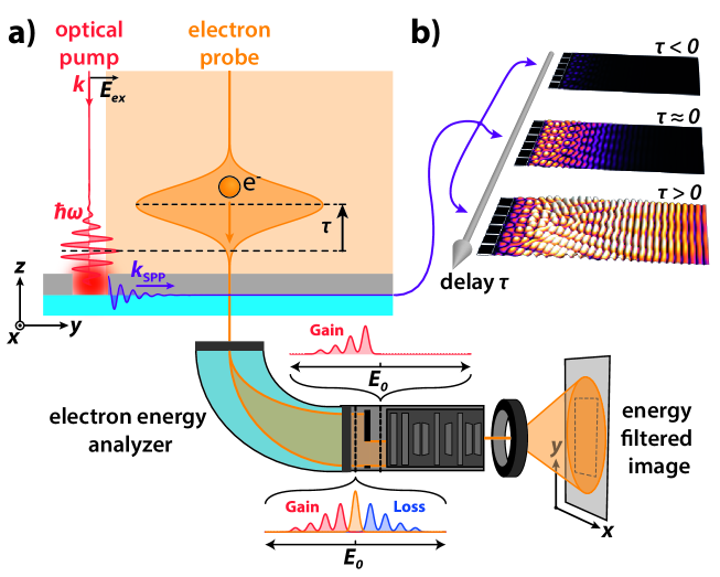
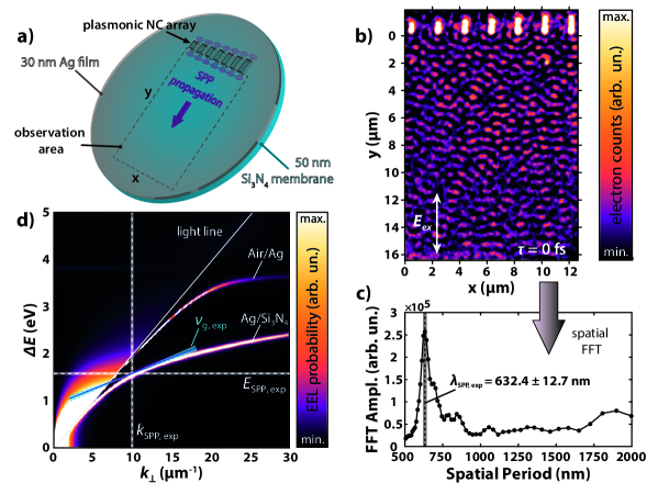
A conceptual scheme of our experiment is sketched in Fig. 1a. A linearly polarized optical pump pulse is incident on a nanocavity in a \ceSi3N4-supported Ag thin film, launching SPPs of energy = that are confined to the Ag/\ceSi3N4 interface. At a variable time delay , the propagating plasmonic wave is then probed by a spatially dispersed pulse of fast electrons, which inelastically scatter from the optically excited SPPs. This scattering interaction results in the electrons gaining and losing integer numbers of SPP energy quantagarcia10_2 ; park10 ; asenjo13 ; feist15 , yielding equidistantly spaced peaks in the energy distribution of the transmitted electrons. By subsequently constructing an energy-filtered image using only those electrons that have gained energy, one directly obtains a spatially-resolved snapshot of the component of the buried plasmonic near-fieldbarwick09 ; barwick15 . Due to the large field-of-view of the electron beam employed here, snapshots recorded at different relative time delays thus capture the spatiotemporal evolution of the photoinduced plasmonic wave (see Fig. 1b).
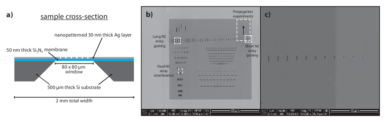
The sample studied in this work consists of a 30 nm Ag thin film deposited on a 50 nm \ceSi3N4 membrane. A variety of different rectangular nanocavity (NC) arrays were patterned into the Ag film using focused ion beam milling (see Methods and Supplementary Figure 1). In order to experimentally measure the propagation speed of SPPs at the buried interface, we monitor a large, featureless area adjacent to a linear array of NCs, as sketched in Fig. 2a. The optical pump beam ( , = 786 nm, full-width-half-maximum (FWHM) duration 105 fs) and the photoelectron probe beam ( 40 ), = 200 keV, FWHM duration 650 fs) are spatially overlapped at near-normal incidence on the Ag side of the nanopatterned bilayer sample. The optical pump pulses generate SPPs at the edges of the NCs, with each edge coupling to the incident electric field component along the in-plane edge normallalanne06 . Since the NCs fully perforate the metal film, photoexcited SPPs are transmitted through the NCs to the other side of the Ag layer and subsequently launched across the Ag/\ceSi3N4 interfacelin13 . In first approximation, each NC edge thus effectively acts as a source of SPPs that travel radially outward in a point dipole-like pattern at the buried interfacetanemura11 . Consequently, according to the Huygens-Fresnel principle, the interferometric plasmonic wave propagating away from the NC array (along the y-axis in Fig. 2a) corresponds to the coherent superposition of the SPPs launched from the different NCs.
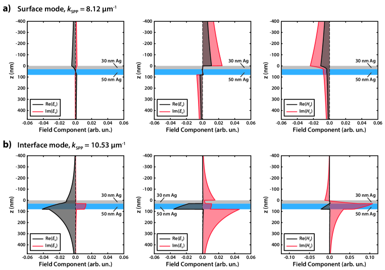
Figure 2b shows the experimental PINEM image of the resulting plasmonic interference pattern (PIP), recorded at a zero relative delay time between the optical pump and electron probe pulse maxima. The spatial fast Fourier transform (FFT) of the entire frame in Fig. 2b gives direct access to the spatial frequencies present in the interference patterngersen05 , and its radial integral is singularly peaked at the spatial period corresponding to the wavelength of the optically driven SPP wave (Fig. 2c). We can thus directly extract the SPP wavelength and wavevector as 633 13 nm and 9.94 0.20 m-1, respectively, where the errors are due to the uncertainty in the calibration of the PINEM image (see Methods). Figure 2d depicts the calculated electron energy loss probability for 200 keV electrons transmitted through a model of our layered sample (30 nm Ag on 50 nm \ceSi3N4), plotted as a function of energy loss and momentum transfer normal to the beam direction. Given the known energy of the optically driven SPPs in the measurements ( = = 1.58 0.015 eV), we find that the experimentally obtained SPP characteristics match well with the theoretical dispersion of the plasmonic mode propagating at the buried interface (see Supplementary Figure 2).
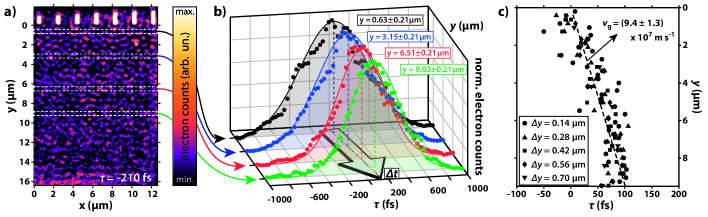
Since PINEM is an ultrafast field-of-view technique, it can track the evolution of the photoexcited plasmonic wave in time, given a sufficient combined spatiotemporal resolution. Here we can follow its evolution and build-up as it propagates away from the linear NC array upon photoexcitation by performing a slice analysis of the PINEM images obtained at different time delays . As sketched in Figure 3a, we divide up the image in a series of horizontal slices centered at different distances from the NC array. By taking the spatial FFT of these slices for each delay, and integrating the Fourier features corresponding to the SPP interference, we can track the propagation of the plasmonic wavefront in time, as is sketched for a number of discrete slices in Fig. 3b. These time traces correspond to the sub-ps cross-correlation of the electron probe and the photoexcited SPP pulse in the different discrete -ranges in the sample, offset by a temporal difference due to the SPP wave propagation. Combining the data of all slices yields a quantitative description of the dynamic behavior, which directly captures the SPP propagation. Figure 3c depicts the temporal center of Gaussian fits to the cross-correlation time traces of different slicing schemes as a function of the distance from the NC array. The linear slope of this curve is a direct measure of the group velocity of the composite plasmonic wave, corresponding to approximately a third of the free-space speed of light, = (9.4 1.3) 107 m s-1. This value is consistent with that expected from theory for the buried SPP mode, as indicated in Figure 2d. Although SPP group velocities at surfaces have been previously extracted from both time domainbai04 and frequency domaintemnov07 experiments, this experiment demonstrates the direct measurement of the SPP propagation speed at a buried interface.
III Shaping transient plasmonic interference patterns
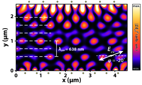
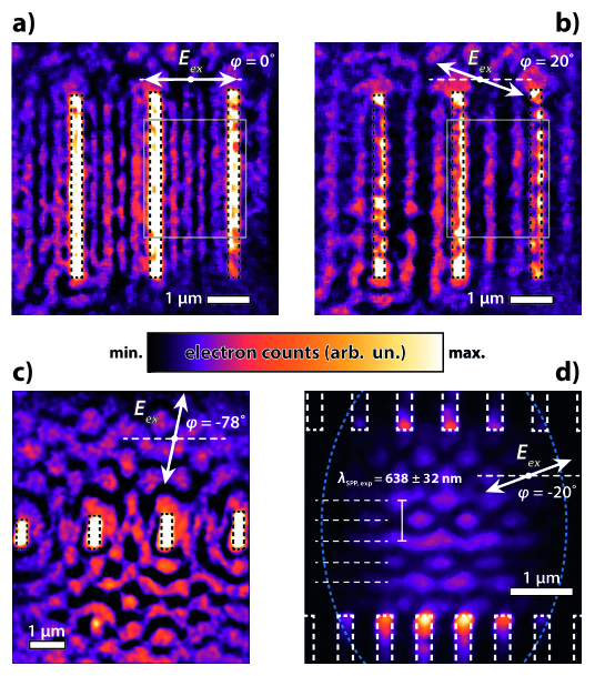
The ability of PINEM to directly access plasmonic interference patterns opens up a multitude of possibilities for creating arbitrarily shaped plasmonic transient gratings, as the obtained interferometric structures can be precisely tailored by combining appropriately arranged nanoscale features with suitable photoexcitationtanemura11 ; lin13 . Moreover, experiments can be supported by simulations applying Maxwell’s equations to the nanopattern architectures, providing effective feedback and enabling the predictive design of transient PIPs. Figure 4 illustrates this flexibility in designing transient PIPs. Panels a and b show the PINEM image of a linear array of long NCs under photoexcitation using different linear polarization orientations, demonstrating that it is indeed possible to obtain transient plasmonic gratings using relatively simple nanostructures. More complex interference patterns can be generated away from such linear NC arrays, as shown for example for an array formed by short NCs (Fig. 4c). One particularly interesting feature of an SPP wave propagating away from a periodic source array is the plasmon Talbot effect, in which the source configuration is self-imaged into an array of plasmon focal spots at characteristic propagation distancesdennis07 . This is predicted to occur even outside the paraxial regime, and upon close inspection its signature can indeed be seen in Figure 2b at , corresponding to the half-period shifted revival at half the so-called Talbot distance. By combining two linear NC arrays with an appropriate relative positioning and photoexcitation one can exploit this effect even at shorter propagation distances, allowing for the generation of multiple closely spaced arrays of nanoscale focal spots of near-field intensity, and thus charge density, at the buried \ceAg/Si3N4 interface (see Fig. 4d). Here the PIP is dominated by the interference of counter-propagating SPPs generated at the different arrays, such that its /2 periodicity along the propagation axis yields = 638 32 nm, which is consistent with the value extracted in Figure 2. Given the thin metal layer and relatively narrow NCs, the influence of multiple scattering and reflections of the SPPs on the structure of the resulting standing wave pattern is small, such that a simple analytical model based on a double array of point dipole SPP sources can reproduce the major features observed (see Supplementary Figure 3). By contrast, this model does not capture the observed complex interference of co-propagating SPPs (as in the propagation experiment). In this case, the time-averaged interference between SPPs from the different point-dipole sources is weaker (similar to that in the plasmon Talbot effect), and additional experimental factors such as non-uniform time-averaging (due to the optical pulse envelope), finite bandwidth excitation and multiple order PINEM scattering are expected to play a dominant role.
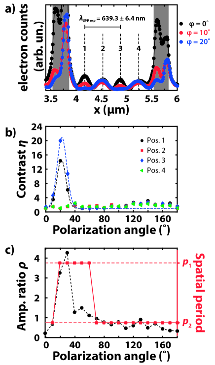
As shown in Fig. 4a-b, the shape of the transient SPP grating generated by the linear array of long NCs is strongly dependent on the excitation polarization. Figure 5 analyzes the indicated region in more detail. In particular, we show in Fig. 5a that upon photoexcitation using light polarized perpendicular to the NC long axis, the counterpropagating SPPs between the NCs set up a transient plasmonic grating with a period corresponding to half the SPP wavelength. This yields another independent determination of the SPP carrier wavelength ( = 639 6 nm), in good agreement with both previously extracted values and the calculated dispersion for the SPP mode propagating at the \ceAg/Si3N4 interface. Interestingly, varying the polarization angle of the incident light dramatically changes the relative intensities of the near-field grating fringes. At a polarization angle of , two of the grating fringes are almost completely suppressed, such that the periodicity of the plasmonic grating has effectively doubled. This is further illustrated in Figs. 5b and c, which depict the full polarization dependence of the transient plasmonic grating. Panel b plots the fringe contrast , calculated as /, for each of the four fringes indicated in Fig. 5a, revealing a clear intensity dip in the -dependence of peaks 1 and 3 centered around . Figure 5c depicts a Fourier analysis of the SPP grating, with the dominant spatial period of the grating indicated by the red squares (right vertical axis) and the grating amplitude ratio (defined as the ratio of FTT amplitudes A(p1)/A(p2) at spatial periods pi = ) indicated by the solid black circles (left vertical axis). These results demonstrate that it is possible to reversibly switch the periodicity of the transient plasmonic grating by tuning the light polarization, showing great promise as a potential means for ultrafast switching of localized charge density in quasi-two-dimensional (quasi-2D) materials and heterostructures.
IV Discussion and Outlook
The unique combination of characterization and control capabilities offered by PINEM enables new scenarios for nanoplasmonic circuits. Advanced nanopatterning and multilayered designs could be used to exploit the quantum entanglement of plasmons altewischer02 ; fakonas14 , efficient plasmon sources based on the quantum Čerenkov effectkaminer15 ; genevet15 or local nonlinear effects at topological defectsyin14 , to name a few. The emergence of 2D solids such as graphenenovoselov12 , hexagonal BNpakdel14 and the layered transition metal dichalcogenideswang12b , their integration into heterostructuresbritnell13 ; gong14 , and the availability of new plasmonic materialswang15 offer a comprehensive set of tools to develop and advance plasmon-based technology in a wide range of areas, including plasmonic sensingstewart08 , nonlinear plasmonicskauranen12 , and plasmonic lasers (SPACERS)zhou13 . Furthermore, the ability to control the spatial shape and temporal evolution of confined plasmonic fields enables the implementation of nanoscale experiments to showcase fundamental properties of quantum mechanicspiazza15 and coherently manipulate electron beamsfeist15 . In analogy to the Kapitza-Dirac effectkapitza33 ; freimund01 , describing the interaction between photons and electrons in free space, it was recently shown in Ref. 57 that electron diffraction from standing plasmon waves can be feasible under experimental conditions similar to those achieved in PINEM, paving the way to the active control of electron diffraction for the generation of tailored beams (e.g. vortex beams) and other exotic superpositions of electron wave-functions.
Summarizing, in this work we demonstrate the in-situ visualization of photoinduced plasmonic interference patterns confined to otherwise inaccessible buried interfaces, enabling a critical tool for the investigation and development of complex plasmonic heterostructures and advanced multilayer devices. Our experiments demonstrate the feasibility of ultrafast imaging of plasmon dynamics using PINEM, allowing us to experimentally measure the carrier wavelength and propagation speed of SPPs traveling at buried interfaces directly in the time domain. Furthermore, we show that transient plasmonic interference patterns can be shaped, manipulated and controlled through both the polarization of the excitation light and the nanopatterning architecture, thus facilitating a widely tunable range of nanoscale near-field structures. Finally, the results presented here represent a considerable advance toward the realization of the recently proposed methodology involving inelastic electron diffraction from transient plasmonic gratings.
Methods
IV.1 Materials.
A silver thin film was sputtered onto an in-house fabricated \ceSi3N4-on-Si support using an EMITECH K575x sputter coater equipped with an Ag target (100 mA, 60s exposure, 3 10-4 mbar base pressure). The nominal thickness of the \ceSi3N4 membrane was 50 nm, with potential thickness variation between 35 and 50 nm. Nanopatterns were written in the Ag layer using a raster-scanned focused-ion beam (FEI Nova Nanolab 200 FIB/SEM) with typical beam currents of 9-10 pA at a 30 kV voltage. Supplementary Figure 1b-c shows an SEM characterization of the sample, which was kept in low oxygen conditions and measured in the UTEM (at 295 K and 10-5 Pa) within a few days of patterning in the FIB. For the propagation experiment, nominal NC widths were 250 nm (experimentally measured (SEM) widths 274 nm) with nominal NC lengths incrementing from 700 to 1300 nm in 100 nm steps (from left to right, NCs in field of view in Fig. 3a, experimentally measured (SEM) lengths (): 698, 809, 919, 982, 1113, 1175, and 1273 nm).
IV.2 Experimental.
A 300 kHz train of linearly polarized light pulses was split to yield two beams, one of which was frequency-tripled to deliver few-nJ UV pulses (262 nm) to a custom truncated-cone \ceLaB6 photo-cathode ( diameter flat tip, produced by AP-Tech) in a custom-modified ultrafast transmission electron microscope (UTEM)piazza13 . The UV pulse train was attenuated to -range average power to ensure photoemission of ultrafast 200 keV single-electron bunches, minimizing electron-electron interactions in the probe and yielding an optimized beam coherence at an electron bunch duration of 650 fs FWHM (bunch envelope proportional to , where is the relative time delay of the electron bunch with respect to the optical pump pulse, see Figure 1). The second optical beam (FWHM duration 105 fs, central wavelength = 786 15 nm), after undergoing a variable delay, was weakly focused on the sample in the UTEM at near-normal incidence using an achromatic doublet ( = 250 mm) to a spot size of diameter at the sample plane, such that the electric field of the pump beam was uniform across the field of view of the electron beam. The time delay is defined as the arrival time of the midway point of the Gaussian electron probe pulse at the sample -position with respect to that of the Gaussian optical pump pulse. Optical pump fluences employed were of the order of 1 to 4 mJ cm-2, corresponding to a peak excitation energy density of 50 GW cm-2. Under these experimental conditions, the generation of SPPs by the transient electric field associated with the electron probe beam is a much weaker effect, which can be considered negligiblepark10 . A detailed description and characterization of the modified JEOL JEM 2100 microscope can be found elsewherepiazza13 . For the PINEM experiments described in this work, the UTEM was operated at 200 keV in photoelectron mode. The GIF imaging camera was operated with a 0.05 eV-per-channel dispersion setting, while typical exposure times of the 20482048 pixel CCD sensor were 60 s for images and 10 s for spectra. Electron energy loss spectra were aligned based on their zero loss peak (ZLP) positions using a differential-based maximum intensity alignment algorithm.
IV.3 Image processing.
Variable delay PINEM frames were spatially aligned using a custom video stabilization algorithm. All obtained PINEM images were median-filtered for single pixel noise and spike removal, and background subtracted using a high-pass spatial-frequency Fourier filter. PINEM image calibration was done using the SEM-measured NC lengths in the field of view as independent references, with the final nm-per-pixel parameter taken as the mean of the calibration factors independently determined for the different NCs. The resulting uncertainty in the image scale is the principal contribution to the error bars on the extracted and values. The fringe positions in Figures 4d and 5a were determined by fitting Gaussian lineshapes to the corresponding integrated spatial traces (the image in Fig. 4d was horizontally integrated), and the resulting values were calculated from the average fringe spacing. Light polarization angles at the sample position inside the UTEM were determined to be within a systematic error of 5∘ and verified by comparison to simulations of the plasmonic field.
For a robust determination of the SPP group velocity, the positive -range of PINEM images recorded at different time delays were divided up into a series of discrete horizontal slices, according to various slicing schemes. The data in Fig. 3b correspond to the spatial FFT analysis of a series of slices with a -range of = . For each slice, a Gaussian temporal profile was fitted to the -dependence of the integrated intensity of the spatial FFT features characteristic of the SPP interference. Full slicing analyses were carried out for slicing schemes having a = 0.14, 0.28, 0.42, 0.56 and , in each case with a -center offset equal to 0.5 (50% slice overlap). The resulting data points (fitted temporal Gaussian center vs. -range center) for each of the slices in the different slicing schemes were combined and fitted with a single straight line, whose slope represents the group velocity of the propagating plasmonic wave (see Fig. 3c).
IV.4 Analytical calculations.
The dispersion diagram in Fig. 2d represents the energy-loss- and in-plane-momentum-transfer-resolved loss probability experienced by an electron crossing the Ag/\ceSi3N4 structure of the experimental sample under normal incidence. The probability is calculated analytically following the methods described in Ref. 24. In brief, (1) the total energy loss is obtained by integrating along the trajectory of the retarding force produced by the induced electric field that is created by the electron and acting back on it; (2) the result is expressed as a double integral over energy- () and momentum-transfer () components, which are interpreted as times the energy-and-momentum-resolved distribution of the loss probability (i.e., the quantity actually represented in the figure); (3) the induced field is in turn obtained by considering a source field produced by the electron in each of the media as if it were moving in an extended homogeneous material; (4) this source field is then scattered at each of the interfaces, where it produces TM reflected waves (note that the source field does not couple to TE waves due to the =0 axial symmetry of the problem for normal electron incidence); (5) the amplitudes of these reflected waves are determined by the continuity of the electric field and the normal displacement; (6) finally, the integral of the retarding force along the trajectory is carried out analytically within each material for every combination of and . The materials (Ag and \ceSi3N4) are represented through their dielectric functions, taken from tabulated measured data (Refs. 58 and 59, respectively).
An approximate plasmonic interference pattern for the nanostructure imaged in Figure 4d was analytically calculated based on arrays of simple point dipole SPP sources (see Supplementary Figure 3). The model takes into
account the finite propagation distance , defined as the decay distance of the plasmon electric field, calculated from the tabulated permittivities for SPPs at a Ag/\ceSi3N4 interface (semi-infinite slabs) at the photon energy under consideration. This value is consistent with the experimental observations in this work, which show little spatial plasmonic field decay within the field of view. All sources were assumed to be monochromatic ( = 638 nm), radiating SPP waves travelling radially outward in a dipolar pattern. All dipoles were oriented along the same direction (maximum radiated field along , with the point dipole oscillating along the perpendicular direction, i.e. ). The resulting complex -field components originating from the different sources were coherently summed, after which uniform time-averaging was incorporated by taking the square modulus of the sum.
References
- (1) Maier, S. A. Plasmonics: Fundamentals and Applications. Springer US, New York, 1 edition, (2007).
- (2) Barnes, W. L., Dereux, A., and Ebbesen, T. W. Nature 424, 824–830 (2003).
- (3) Ozbay, E. Science 311, 189–193 (2006).
- (4) Stewart, M. E., Anderton, C. R., Thompson, L. B., Maria, J., Gray, S. K., Rogers, J. A., and Nuzzo, R. G. Chemical Reviews 108(2), 494–521 (2008).
- (5) Liu, X., Wang, Y., and Potma, E. O. Applied Physics Letters 101(8), 081116 (2012).
- (6) Bohm, C., Bangert, J., Mertin, W., and Kubalek, E. Journal of Physics D: Applied Physics 27(10), 2237 (1994).
- (7) Gersen, H., Karle, T. J., Engelen, R. J. P., Bogaerts, W., Korterik, J. P., van Hulst, N. F., Krauss, T. F., and Kuipers, L. Phys. Rev. Lett. 94, 073903 Feb (2005).
- (8) Wagner, M., McLeod, A. S., Maddox, S. J., Fei, Z., Liu, M., Averitt, R. D., Fogler, M. M., Bank, S. R., Keilmann, F., and Basov, D. N. Nano Letters 14(8), 4529–4534 (2014).
- (9) Nishiyama, Y., Imura, K., and Okamoto, H. Nano Letters 15(11), 7657–7665 (2015).
- (10) Petek, H. and Ogawa, S. Progress in Surface Science 56(4), 239 – 310 (1997).
- (11) Kubo, A., Onda, K., Petek, H., Sun, Z., Jung, Y. S., and Kim, H. K. Nano Letters 5(6), 1123–1127 (2005).
- (12) Kubo, A., Pontius, N., and Petek, H. Nano Letters 7(2), 470–475 (2007).
- (13) Aeschlimann, M., Bauer, M., Bayer, D., Brixner, T., Cunovic, S., Dimler, F., Fischer, A., Pfeiffer, W., Rohmer, M., Schneider, C., Steeb, F., Strüber, C., and Voronine, D. V. Proceedings of the National Academy of Sciences 107(12), 5329–5333 (2010).
- (14) Lemke, C., Schneider, C., Leißner, T., Bayer, D., Radke, J. W., Fischer, A., Melchior, P., Evlyukhin, A. B., Chichkov, B. N., Reinhardt, C., Bauer, M., and Aeschlimann, M. Nano Letters 13(3), 1053–1058 (2013).
- (15) Lemke, C., Leißner, T., Evlyukhin, A., Radke, J. W., Klick, A., Fiutowski, J., Kjelstrup-Hansen, J., Rubahn, H.-G., Chichkov, B. N., Reinhardt, C., and Bauer, M. Nano Letters 14(5), 2431–2435 (2014).
- (16) Gong, Y., Joly, A. G., Hu, D., El-Khoury, P. Z., and Hess, W. P. Nano Letters 15(5), 3472–3478 (2015).
- (17) Mårsell, E., Losquin, A., Svürd, R., Miranda, M., Guo, C., Harth, A., Lorek, E., Mauritsson, J., Arnold, C. L., Xu, H., L’Huillier, A., and Mikkelsen, A. Nano Letters 15(10), 6601–6608 (2015). PMID: 26375959.
- (18) Bauer, M., Wiemann, C., Lange, J., Bayer, D., Rohmer, M., and Aeschlimann, M. Applied Physics A 88(3), 473–480 (2007).
- (19) Lemke, C., Leißner, T., Jauernik, S., Klick, A., Fiutowski, J., Kjelstrup-Hansen, J., Rubahn, H.-G., and Bauer, M. Opt. Express 20(12), 12877–12884 Jun (2012).
- (20) Kociak, M., Stéphan, O., Walls, M. G., Tencé, M., and Colliex, C. Scanning Transmission Electron Microscopy: Imaging and Analysis, chapter Spatially Resolved EELS: The Spectrum-Imaging Technique and Its Applications, 163–205. Springer New York, New York, NY (2011).
- (21) Bosman, M., Keast, V. J., Watanabe, M., Maaroof, A. I., and Cortie, M. B. Nanotechnology 18(16), 165505 April (2007).
- (22) Nelayah, J., Kociak, M., Stéphan, O., García de Abajo, F. J., Tencé, M., Henrard, L., Taverna, D., Pastoriza-Santos, I., Liz-Marzán, L. M., and Colliex, C. Nat. Phys. 3(5), 348–353 (2007).
- (23) Schaffer, B., Hohenester, U., Trügler, A., and Hofer, F. Phys. Rev. B 79, 041401 Jan (2009).
- (24) García de Abajo, F. J., Rivacoba, A., Zabala, N., and Yamamoto, N. Phys. Rev. B 69, 155420 Apr (2004).
- (25) Rossouw, D. and Botton, G. A. Phys. Rev. Lett. 110, 066801 Feb (2013).
- (26) Barwick, B., Flannigan, D. J., and Zewail, A. H. Nature 462, 902–906 (2009).
- (27) García de Abajo, F. J., Asenjo-Garcia, A., and Kociak, M. Nano Letters 10(5), 1859–1863 (2010).
- (28) Park, S. T., Lin, M., and Zewail, A. H. New J. Phys. 12(12), 123028 (2010).
- (29) Park, S. T. and Zewail, A. H. Phys. Rev. A 89, 013851 Jan (2014).
- (30) Piazza, L., Masiel, D. J., LaGrange, T., Reed, B. W., Barwick, B., and Carbone, F. Chem. Phys. 423(8), 79–84 (2013).
- (31) Barwick, B. and Zewail, A. H. ACS Photonics 2(10), 1391–1402 (2015).
- (32) Piazza, L., Lummen, T., Quiñonez, E., Murooka, Y., Reed, B. W., Barwick, B., and Carbone, F. Nat. Commun. 6, 6407 (2015).
- (33) Feist, A., Echternkamp, K. E., Schauss, J., Yalunin, S. V., Schäfer, S., and Ropers, C. Nature 521, 200–203 (2015).
- (34) Hassan, M. T., Liu, H., Baskin, J. S., and Zewail, A. H. Proceedings of the National Academy of Sciences 112(42), 12944–12949 (2015).
- (35) Asenjo-García, A. and García de Abajo, F. J. New J. Phys. 15(10), 103021 (2013).
- (36) Lalanne, P., Hugonin, J. P., and Rodier, J. C. J. Opt. Soc. Am. A 23(7), 1608–1615 Jul (2006).
- (37) Lin, J., Mueller, J. P. B., Wang, Q., Yuan, G., Antoniou, N., Yuan, X.-C., and Capasso, F. Science 340(6130), 331–334 (2013).
- (38) Tanemura, T., Balram, K. C., Ly-Gagnon, D.-S., Wahl, P., White, J. S., Brongersma, M. L., and Miller, D. A. B. Nano Letters 11(7), 2693–2698 (2011).
- (39) Bai, M., Guerrero, C., Ioanid, S., Paz, E., Sanz, M., and García, N. Phys. Rev. B 69, 115416 Mar (2004).
- (40) Temnov, V. V., Woggon, U., Dintinger, J., Devaux, E., and Ebbesen, T. W. Opt. Lett. 32(10), 1235–1237 May (2007).
- (41) Dennis, M. R., Zheludev, N. I., and García de Abajo, F. J. Opt. Express 15(15), 9692–9700 Jul (2007).
- (42) Altewischer, E., van Exter, M. P., and Woerdman, J. P. Nature 418(6895), 304–306 (2002).
- (43) Fakonas, J. S., Lee, H., Kelaita, Y. A., and Atwater, H. A. Nat. Photon. 8(4), 317–320 (2014).
- (44) Kaminer, I., Tenenbaum Katan, Y., Buljan, H., Shen, Y., Ilic, O., López, J. J., Wong, L. J., Joannopoulos, J. D., and Soljačić, M. ArXiv e-prints , arXiv:1510.00883 oct (2015).
- (45) Genevet, P., Wintz, D., Ambrosio, A., She, A., Blanchard, R., and Capasso, F. Nat. Nanotechnol. 10, 804–809 (2015).
- (46) Yin, X., Ye, Z., Chenet, D. A., Ye, Y., O’Brien, K., Hone, J. C., and Zhang, X. Science 344(6183), 488–490 (2014).
- (47) Novoselov, K. S., Fal’ko, V. I., Colombo, L., Gellert, P. R., Schwab, M. G., and Kim, K. Nature 490(7419), 192–200 (2012).
- (48) Pakdel, A., Bando, Y., and Golberg, D. Chem. Soc. Rev. 43, 934–959 (2014).
- (49) Wang, Q. H., Kalantar-Zadeh, K., Kis, A., Coleman, J. N., and Strano, M. S. Nat. Nanotechnol. 7(11), 699–712 (2012).
- (50) Britnell, L., Ribeiro, R. M., Eckmann, A., Jalil, R., Belle, B. D., Mishchenko, A., Kim, Y.-J., Gorbachev, R. V., Georgiou, T., Morozov, S. V., Grigorenko, A. N., Geim, A. K., Casiraghi, C., Neto, A. H. C., and Novoselov, K. S. Science 340(6138), 1311–1314 (2013).
- (51) Gong, Y., Lin, J., Wang, X., Shi, G., Lei, S., Lin, Z., Zou, X., Ye, G., Vajtai, R., Yakobson, B. I., Terrones, H., Terrones, M., Tay, B., Lou, J., Pantelides, S. T., Liu, Z., Zhou, W., and Ajayan, P. M. Nat. Mater. 13(12), 1135–1142 (2014).
- (52) Wang, Y., Capretti, A., and Negro, L. D. Opt. Mater. Express 5(11), 2415–2430 Nov (2015).
- (53) Kauranen, M. and Zayats, A. V. Nat. Photon. 6(11), 737–748 (2012).
- (54) Zhou, W., Dridi, M., Suh, J. Y., Kim, C. H., Co, D. T., Wasielewski, M. R., Schatz, G. C., and Odom, T. W. Nat. Nano. 8(7), 506–511 (2013).
- (55) Kapitza, P. L. and Dirac, P. A. M. Proc. Camb. Phil. Soc. 29, 297–300 (1933).
- (56) Freimund, D. L., Aflatooni, K., and Batelaan, H. Nature 413(6852), 142–143 (2001).
- (57) García de Abajo, F. J., Barwick, B., and Carbone, F. ArXiv e-prints , arXiv:1603.07551 mar (2016).
- (58) Johnson, P. B. and Christy, R. W. Phys. Rev. B 6, 4370–4379 Dec (1972).
- (59) Palik, E. D., editor. Handbook of Optical Constants of Solids. Academic Press Limited, London, (1998).
Supplementary Figures