First-principle calculations of phononic, electronic and optical properties of monolayer arsenene and antimonene allotropes
Abstract
Recently a stable monolayer of antimony in buckled honeycomb structure called antimonene was successfully grown on 3D topological insulator Bi2Te3 and Sb2Te3, which displays semiconducting properties. By first principle calculations, we systematically investigate the phononic, electronic and optical properties of and allotropes of monolayer arsenene/antimonene. We investigate the dynamical stabilities of these four materials by considering the phonon dispersions. The obtained electronic structures reveal the direct band gap of monolayer As/Sb and indirect band gap of As/Sb. Significant absorption is observed in Sb, which can be used as a broad saturable absorber.
I INTRODUCTION
Recently two-dimensional materials have been intensely investigated due to the extraordinary properties which can be widely used in the next-generation nanoelectronic and optoelectronic applicationsdoi:10.1021/am501022x ; Aktuerk2015 ; C5CP00563A . Graphene is a honeycomb monolayer of carbon atoms, which possesses superior carrier mobilityPhysRevX.4.021029 , but with a small on-off ratio due to the zero band gap, which limits the applications in electronic devices. Black phosphoreneLiu2014 ; doi:10.1021/nl501658d ; Li2014 , a monolayer of phosphorus atoms with puckered structure, induces great attention recently due to the versatile properties such as direct semiconducting property with a moderate band gaphong2014polarized , a higher hole mobility comparable to grapheneQiao2014 , high carrier mobilitychen2016nonequilibrium , strongly anisotropic transportLiu2014 and etc.
The extraordinary properties and the potential applications in the fields of electronics and optoelectronics of black phosphorene have aroused great research interest on other group-V elemental monolayersPhysRevB.92.125420 ; SMLL201570033 ; zheng2016 ; PhysRevB.91.085423 ; wang2015electronic , considering the chemical similarity of elements belonging to the same group in the periodic table. Monolayers of arsenic and antimony with different phases were thus proposed and under investigation by exprimentsWang2015a ; PhysRevB.91.085423 ; Aktuerk2015 ; Wang2015 . The orthorhombic () arsenene (monolayer of arsenic) was predicted to be a semiconducting material with a direct band gap of approximate 1 eV. The orthorhombic arsenene (As) possesses high carrier mobilityzheng2016 ; Wang2015 and strong anisotropyzheng2016 , which make it promising for device applications in the semiconductor industry and solar cellszheng2016 ; PhysRevB.91.085423 . Monolayer antimonene including and phases are semiconductors with band gaps suitable for their use in 2D electronicsAktuerk2015 . The Sb has nearly isotropic mechanical properties, whereas Sb shows strongly anisotropic charecteristicWang2015 .
Experimentally, antimonene(monolayer of antimony) has been successfully realized on the substrates of 3D topological insulator Bi2Te3 and Sb2Te3 respectively:/content/aip/journal/jap/119/1/10.1063/1.4939281 , and the stability of monolayer antimonene allotropes including , , , and phase were examined by phonon dispersion calculationsWang2015 , which shown that only the monolayer and antimonene (Sb) are stable as free-standing monolayers. However, to our knowledge, monolayer arsenene has not been experimentally realized up to nowPhysRevB.91.085423 . Considering those studies of monolayer and As/Sb, it lacks systematically investigations of the electronic and optical properties of the four materials with two different structures.
In this work, the density functional theory based first-principles calculations are used to investigate the phonon, electronic and optical properties of four two-dimensional materials, i.e. As and Sb. We first optimize the structures and investigate the dynamical stabilities of the optimized structures. Then we calculate the electronic structures of these four materials and show that the value of the band gap of As/Sb is smaller than that of the counterpart by comparison. Finally we calculate the optical properties of these four materials, and find that As/Sb possess strong in-plane anisotropy due to the structure anisotropy, and abundant optical properties. The underlying mechanism of the optical properties is further discussed as well.
II Method and computational details
The calculations are performed using the Vienna ab-initio simulation package (VASP) based on density functional theory Kresse1996 . The calculation is carried out by using the projector-augmented-wave pseudo potential method with a plane wave basis set with a kinetic energy cutoff of 500 eV. The exchange-correlation energy is described by the generalized gradient approximation (GGA) using the Perdew-Burke-Ernzerhof (PBE) functional Perdew1996 . Since the PBE functional always underestimates the band gap of semiconductors, part of the calculations is also performed using the Heyd-Scuseria-Ernzerhof (HSE06) hybrid functional which is constructed by mixing the PBE and Hartree-Fock (HF) fuctionals. HSE06 improves the precision of band gap by reducing the localization and delocalization errors of PBE and HF functions. Here the screening length of HSE06 is 0.2 and the mixing ratio of the HF exchange potential is 0.25.
The Brillouin zone integration is performed with a 15151 k mesh for geometry optimization and self-consistent electronic structure calculationsMa2015 . When optimizing atomic positions under this k mesh, the energy convergence value between two consecutive steps are chosen as 10-6 eV and the maximum Hellmann-Feynman force acting on each atom is less than 10-3 eV/Å.
For and As/Sb, we use periodic boundary conditions along the three dimensions, and the vacuum space is around 28 and 18 along the direction, respectively, which is large enough to avoid the artifical interaction between atom layers. Furthermore, in the ground state, the configuration of extra-nuclear electron of As is 4s24p3 and Sb is 5s25p3, respectively.
The phonon dispersion is calculated from the harmonic IFCs using the PHONOPY codeTogo2008 . A 551 supercell with 551 k mesh is used for and As/Sb to ensure the functional convergence. We also calculate the optical properties of monolayer and As/Sb using PBE method on a grid of 21211 k-points.
III Results and discussion
III.1 Optimized structures of and As/Sb
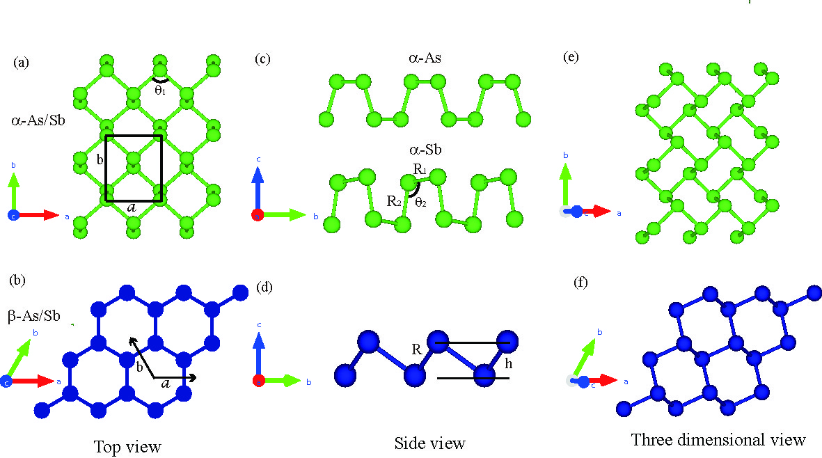
Fig. 1 shows the fully relaxed structures of monolayer and As/Sb. The structures of As and Sb are puckered with the space group and respectively, and consist of four atoms in a unit cell, as shown in Fig. 1(a). From the side view in Fig. 1(c), both As and Sb consist of two atomic sublayers, but for As all the atoms of a sublayer are located in the same plane. The honeycomb structure of monolayer As/Sb is buckled as well with the space group of and consists of two atoms in each unit cell, as shown in Fig. 1(b). The side view of As/Sb in Fig. 1(d) also shows that two atomic sublayers exist in As/Sb, similar to As/Sb.
| / | ||||||||
|---|---|---|---|---|---|---|---|---|
| () | () | () | () | (∘) | (∘) | (eV/atom) | (eV) | |
| -As | 3.68(3.71zheng2016 ) | 4.77(4.67zheng2016 ) | 2.51 | 2.50 | 94.50 | 100.66 | -4.62 | 0.91/0.90 |
| -Sb | 4.36(4.28Aktuerk2015 ) | 4.73(4.74Aktuerk2015 ) | 2.95 | 2.87 | 95.3 | 102.8 | -4.04 | 0.22/0.21 |
| // | ||||||
|---|---|---|---|---|---|---|
| () | () | (∘) | () | (eV/atom) | (eV) | |
| -As | 3.61(3.607PhysRevB.91.085423 ) | 2.51 | 91.95 | 1.40(1.35:/content/aip/journal/apl/107/2/10.1063/1.4926761 ) | -4.65 | 1.59/1.47/2.11 |
| -Sb | 4.12(4.12Wang2015 ) | 2.89 | 90.84 | 1.65(1.66wang2015electronic ) | -4.04 | 1.26/0.99/1.70 |
Table 1 shows the optimized lattice parameters, bond characteristics and cohesive energies of As/Sb. For As, the calculated puckered angle is 100.66∘, which is slightly smaller than that of phosphorene (103.69∘)2053-1583-1-2-025001 . The optimized lattice parameters are = 3.68Å and = 4.77, which are in good agreement with previous theoretical workzheng2016 . The calculated bond lengths are 2.50 and 2.51 with bond angles = 94.50∘ and = 100.66∘ respectively. For Sb, the optimized lattice constants are = 4.36 and = 4.73, which are in good agreement with previous theoretical workAktuerk2015 as well. Since , the crystal structure of As/Sb is anisotropic along and directions.
However, for As, the crystal structure is isotropic along the and directions, i.e. . The optimized lattice parameter and the buckling height between the two sublayers are and respectively, which are in good agreement with previous theoretical resultsPhysRevB.91.085423 ; :/content/aip/journal/apl/107/2/10.1063/1.4926761 . The calculated results lattice parameters and bond characteristics of Sb are shown in Table 2.
III.2 Phonon dispersions and stabilities of and As/Sb
For the experimental realization of these newly proposed 2D materials, the consideration of the stability is required. The necessary condition for the structural stabilities of and As/Sb against low-frequency acoustic vibrations, which will induce long-wavelength transverse/longitudinal displacements in different directions of the BZ, is that all the phonon frequencies are real. The calculated phonon dispersions of and As/Sb are shown in Fig. 2.
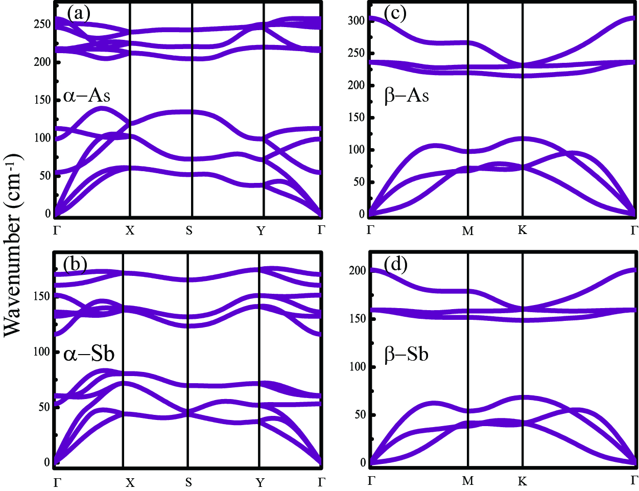
Obviously, there is no imaginary frequency in the obtained phonon dispersion curves for both As/Sb and As/Sb, revealing the dynamical stability of those four materials as free-standing monolayers. The calculated phonon band gap is about 66 cm-1 (As) , 33 cm-1 (Sb), 97 cm-1 (As) and 80 cm-1 (Sb), respectively. Since the phonon band gap of As is larger than that of Sb, more anharmonic three-phonon scatterings among the acoustic phonons and optical phonons in As are suppressed compared to Sb, which means that the corresponding contribution from the anharmonic three-phonon scatterings to the thermal conductivity in As is less important than that in Sb.
In addition, the stability of monolayer and As/Sb can be further examined by the cohesive energy calculations. As listed in Table 1 and 2, the cohesive energies of /As are smaller than the corresponding cohesive energies of /Sb, indicating a stronger As-As bond compared to the Sb-Sb bond which is in agreement with the ELF results.
III.3 Electronic properties of and As/Sb
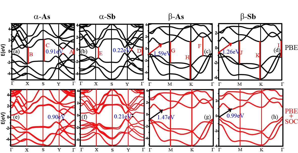
The calculated electronic band structures of monolayer As/Sb and As/Sb along the high-symmetry directions of Brillouin zone (BZ) are shown in Fig. 3. Within the PBE functional method, As is a semiconductor with a direct band gap of 0.91 eV, shown in Fig. 3(a), and the minimum of the conduction band (CBM) and maximum of the valance band (VBM) locate within . The band gap decreases trivially when the spin-orbit coupling (SOC) is involved, as shown in Fig. 3(e). Similar calculations are performed on Sb, shown in Fig. 3(b,f). The band gap of Sb by PBE is 0.22 eV, much smaller than that of As, which may come from the lower bond energy between Sb atoms than As-As bond. The involved SOC effect gives the band gap of 0.21 eV, as shown in Fig. 3(f), and lifts the degeneracy of valence and conduction bands around the Fermi level.
In Fig. 3(c) and (d), we calculate the band structures of monolayer As/Sb, and both of which show an indirect band gap between CBM and VBM locating within . The VBM locates at the point. For As, the band gap calculated within the PBE functional (Fig. 3(c)) is 1.59 eV, reduced to 1.47 eV after SOC effect (Fig. 3(g)) involved, and increases to 2.11 eV by considering the HSE06 (Fig. 3(k)) correction. Similar calculations of Sb show that the band gap of PBE/PBE+SOC/HSE06 is 1.59/1.47/1.70 eV respectively, as shown in Figs. 3(d,h,l).
By comparison to the band stuctures of and As/Sb, it’s found that the band gap of As/Sb is direct while the band gap of As/Sb is indirect, and furthermore, the value of the bandgap of As/Sb is smaller than that of the counterpart. Considering the SOC effects, it is found that the SOC effect influences the and Sb more significantly compared to and As, Which is due to the relatively heavier atoms of antimonene.
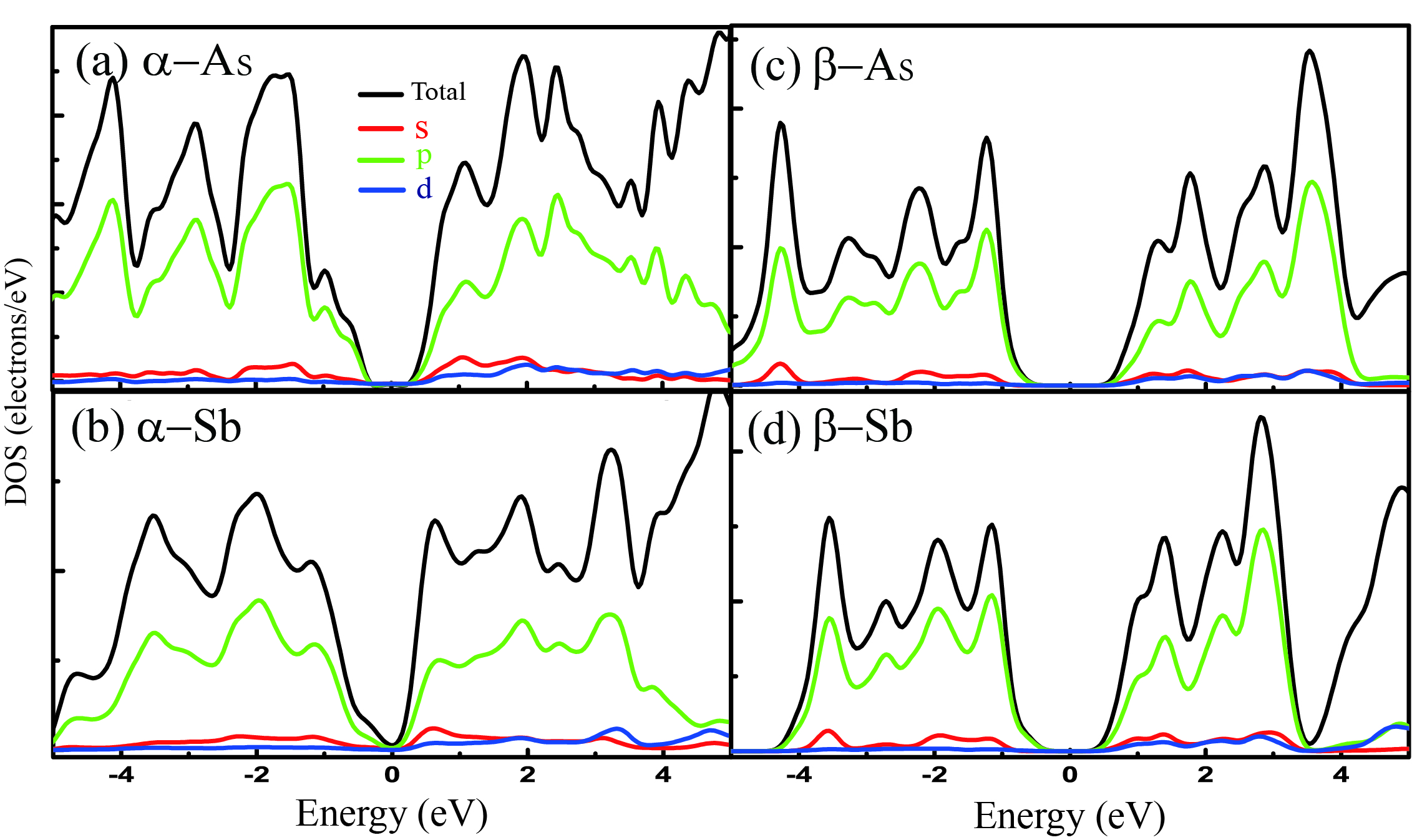
In order to explain the formation of the band gap of and As/Sb and clarify contributions from different orbits, we have calculated the density of state (DOS) of monolayer and As/Sb, as shown in Fig. 4. The total and projected densities of states are calculated as shown in Fig. 4, which indicates that for and As/Sb, the p-orbital electronic states dominate the top of the valence bands and the bottom of the conduction bands.
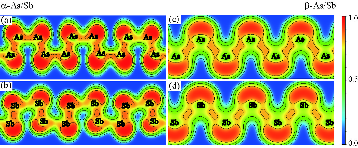
To understand the bonding characteristics, the electron localization function (ELF) Becke1990 ; Savin1992 ; Gatti2005 ; Chen2013 is calculated, as shown in Fig. 5. The ELF is a position dependent function with values that range from 0 to 1. ELF=1 corresponds to perfect localization and ELF=0.5 correponds to the electron-gas like pair probability. The respective ELF profile of As/Sb, as shown in Fig. 5(a) and (b) respectively, is similar to that of the counterpart, as shown in Fig. 5(c) and (d) respectively. Furthermore, although the ELF values increase in regions around the As/Sb sites in all four materials, the ELF values between the atoms in different sublayers in As/Sb is larger than those in As/Sb, which means that the chemical bondings in As/Sb are more covalent compared to As/Sb.
III.4 Optical properties of and As/Sb
The optical properties of monolayer and As/Sb are described by the complex dielectric function, . The imaginary part of dielectric tensor is determined by a summation over empty band states using as follows Gajdos2006 ,
| (1) |
where is the vacuum dielectric constant, is the crystal volume, and represent the valence and conduction bands respectively, is the energy of the incident phonon, u is the vector defining the polarization of the incident electric field, ur is the momentum operator, and are the wave functions of the conduction and valence band at the point, respectively. The real part of dielectric tensor is obtained by the well-known Kramers-Kronig relationdresselhaus1999solid ,
| (2) |
where denotes the principle value. Based on the dielectric function of and As/Sb, the optical properties including the energy loss spectrum can be subsequently given by Saha2000 ; Luo2015 ; peng2016first
| (3) |
| (4) |
| (5) |
Figs.6-8 give the dielectric function , energy loss function , the absorption coefficient and the reflectivity are obtained for both and As/Sb. For the anisotropic As/Sb, only in-plane optical properties are calculated for incident light with the polarization of the electric field E along the (E//) and (E//) directions. While for the isotropic As/Sb, optical properties are calculated for in-plane polarization () and out-plane polarization (), respectively.
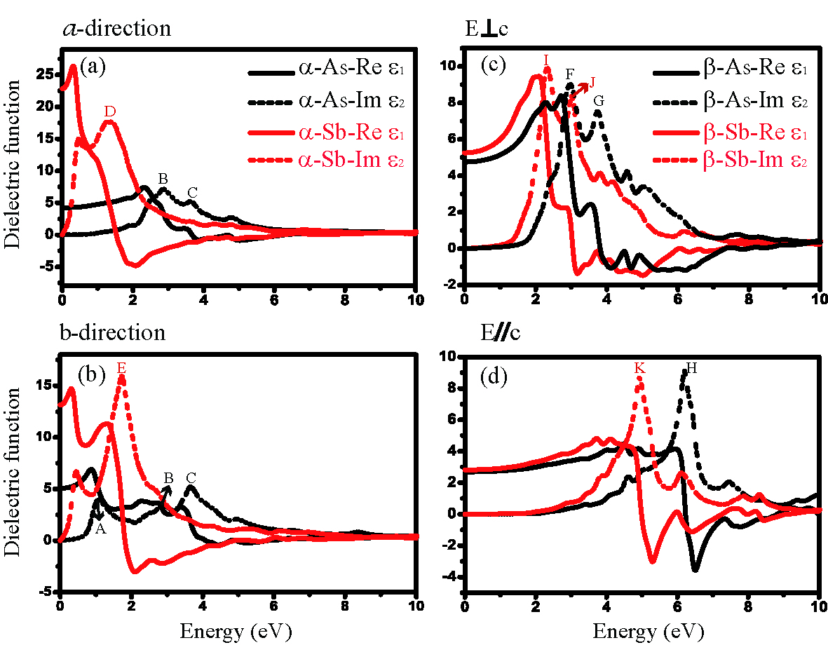
For the dielectric function of As/Sb shown in Fig. 6(a) and (b) respectively, strong in-plane anisotropy () is observed, which is attributed to the anisotropic crystal structure of As/Sb. As we know, the peaks in the imaginary part of dielectric function are caused by the absorption of incident photons and the interband transition of electronsMohan20121670 .
For As, the imaginary part of dielectric function for E// shows peaks at 2.84 eV and 3.64 eV indicated by B and C respectively in Fig. 6(a), while in the curve of for E//, three main peaks at 1.0 eV, 2.86 eV and 3.66 eV indicated by A, B and C respectively are observed in Fig. 6(b). By comparison to the band structure of As shown in Fig. 3(a), the peak A is attributed to the interband transition along direction close to the point. The peak B is probably due to the “paralle band effect” along the direction indicated in Fig. 3(a) Fox2001 . The peak C is associated with the interband transition of electron from the VB to CB near Fermi energy along the direction close to the point shown in Fig. 3(a).
For Sb, in the curves of shown in Fig. 6(a) and (b), for E//, one main peak is observed at 1.33 eV (peak D); for E//, also one main peak is observed at 1.73 eV (peak E). Both peaks are attributed to the interband transition of electron from VB to CB near Fermi energy, as shown in the band structure of Sb in Fig. 3(b).
Similar analysis can be performed to the the imaginary part of dielectric function of As/Sb, and the peaks in the curves of of As/Sb, shown in Fig. 6(c) and (d) respectively, can be attributed to the corresponding interband transitions of electrons indicated in the band structures of As/Sb in Fig. 3(c) and (d) respectively.
By comparison to the dielectric functions between As and Sb, the curves of of As/Sb for E// and E//, shown as the black and red dot lines in Fig. 6(a) and (b), the number of peaks and the profile of curves are roughly similar, except that the curves of As are blueshifted to some extent to those of Sb. A greater similarity and a smaller blueshift are observed between the curves of As and Sb as well, shown as the black and red dot lines in Fig. 6(c) and (d). The similarity existed within the curves of results from the similarity of the band structure of As (As) compared to that of Sb (Sb) as mentioned above, since the imaginary part of dielectric function is determined by the band structure of crystal according to Eq. (1). It is obvious that the simlarity between the band structures of As and Sb, shown in Fig. 3(c) and (d), is greater than that of As and Sb, shown in Fig. 3(a) and (b), as a result, a greater similarity between the the curves of of As and Sb can be thus observed.
Since the major contribution to of semiconductors comes from the interband transitions of electrons from VB to CB near Fermi energydresselhaus1999solid , and the band gap of As is larger than that of Sb, therefore the curves of As is blueshifted compared to those of Sb, as shown in Fig. 6(a) and (b). The observed blueshift in the curves of As compared to those of Sb, as shown in Fig. 6(c) and (d), can be explained in a similar way.
According to the Kramers-Kronig relation, i.e. Eq. (2), the real part of the dielectric function is determined by the imaginary part of the dielectric function , as a result, the above-mentioned similarity and blueshift can be also observed in the curves of As (As) compared to those of Sb (Sb), shown as the black and red solid lines in Fig. 6(a-b) (Fig. 6(c-d)).
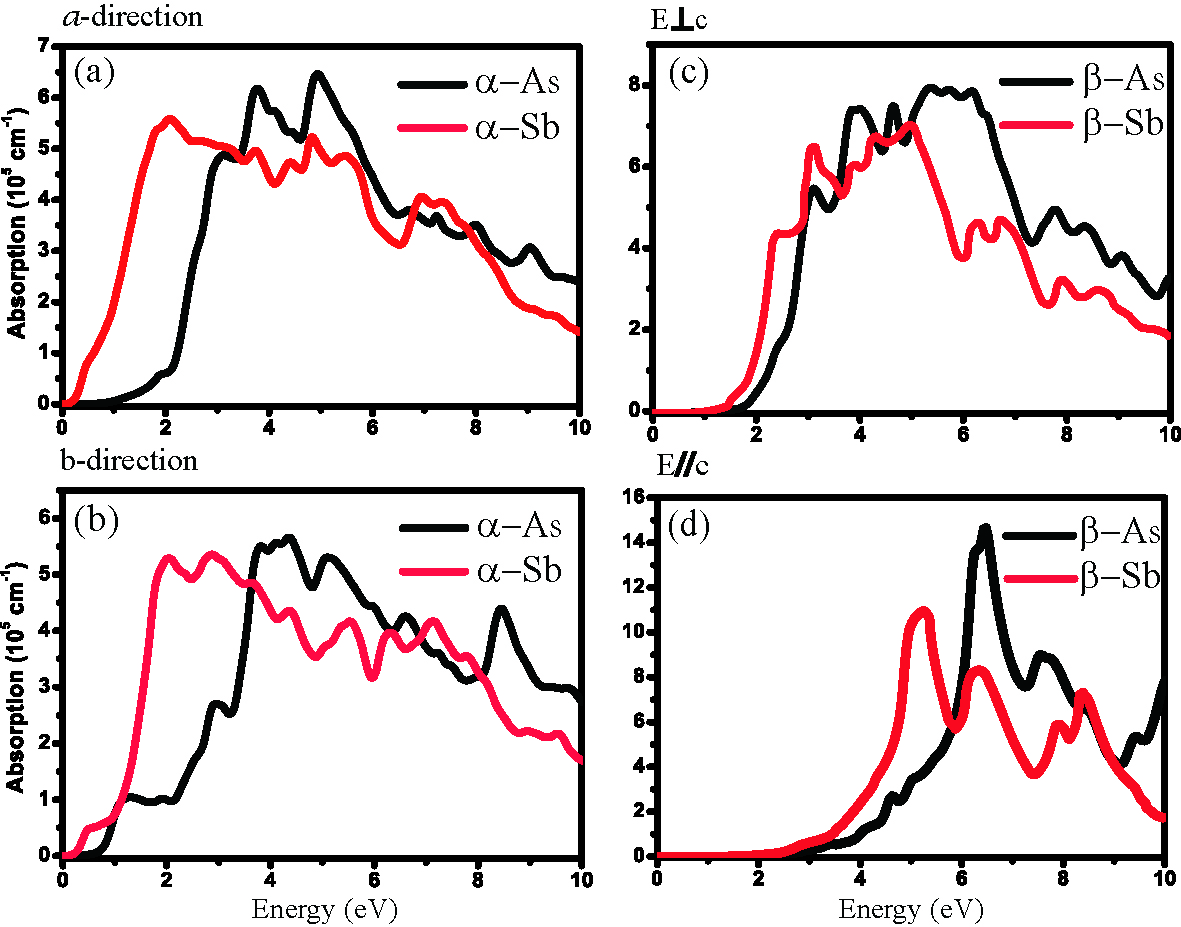
The calculated absorption coefficients for both As/Sb and As/Sb are shown in Fig. 7. The above-mentioned similarity and blueshift are observed as well in the absorption curves of As (As) compared to those of Sb (Sb), except that the absorption bandwidth of antimonene is broader than that of arsenene irrespective of or structure. In addition, significant absorption from the visible region to the ultraviolet region can be observed in Sb, while for As the significant absorption begins in the blue region and ends in the ultraviolet region. So Sb may become an alternative candidate for the application of saturable absorber which can be used in laser device. It should be noted that, the absorption of As/Sb is negligible in the visible region, as shown in Fig. 7(d).
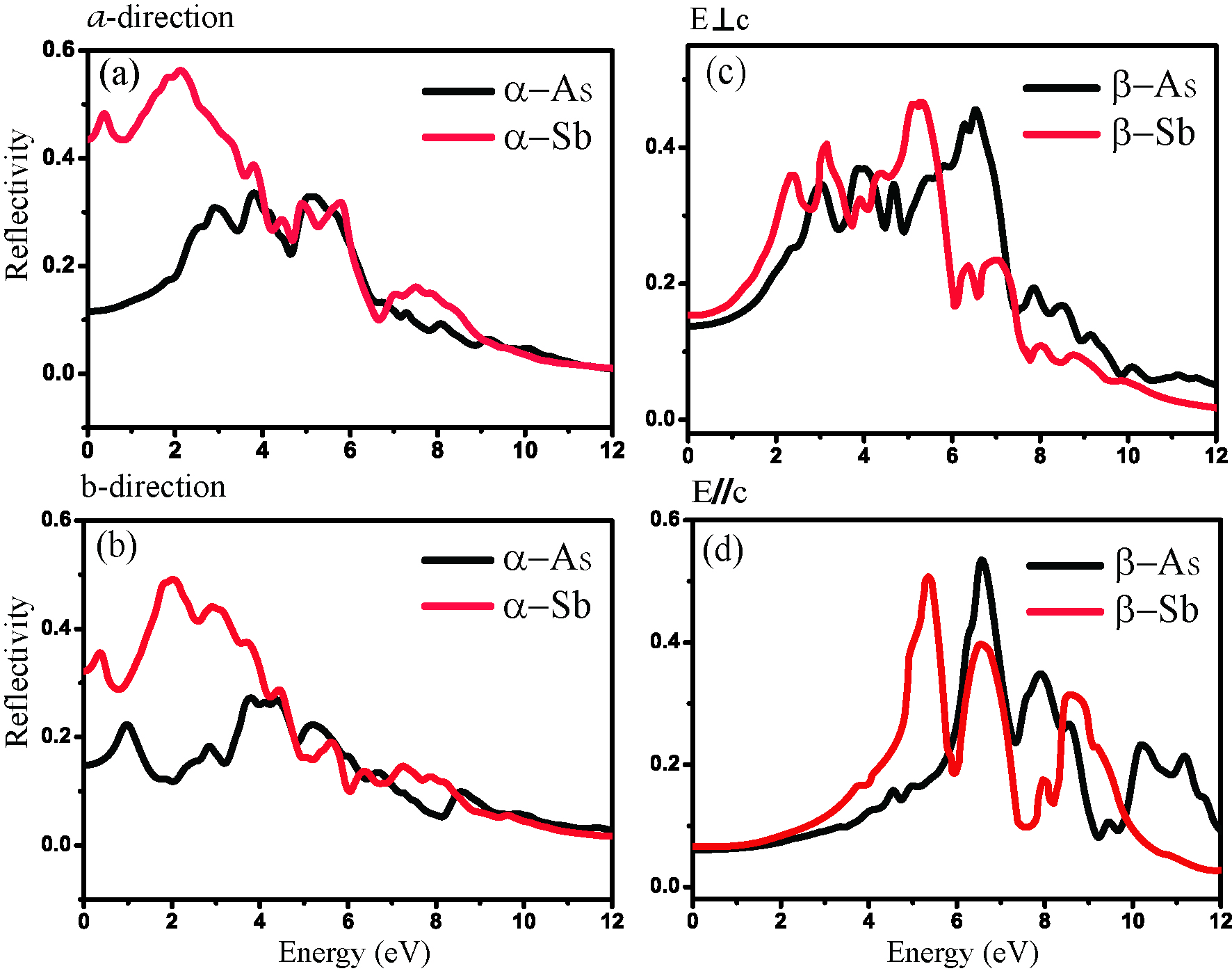
Fig. 8 shows the reflectivity for both As/Sb and As/Sb. It is shown in Fig. 8(a-b) that, for the case of As along both and directions, the reflectivity in the visible region is high. Considering that the absorption in the visible region for As is large too as mentioned above, As is a non-transparent material. However, for As/Sb when E//, the reflectivity in the visible region is low and the absorption in the visible region is negligible, indicating that As/Sb are directionally transparent materials.
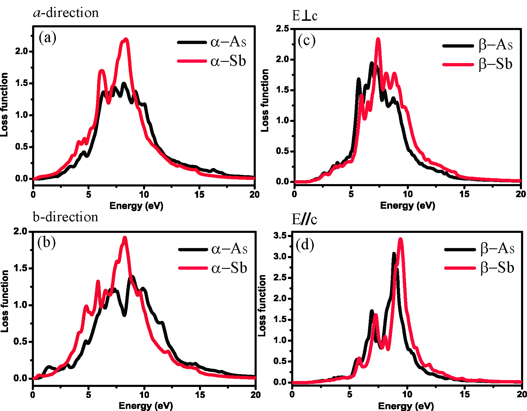
Fig. 9 shows the electron energy loss spectroscopy for both As/Sb and As/Sb. Electron energy loss spectroscopy (EELS) describes the energy lost by electron when passing through dielectric materials, and can be used to deduce the dielectric function of materialsC5CP00563A .
IV Conclusion
In conclusion, we systematically investigate the phonon, optical and electronic properties of monolayer and As/Sb by first-principles calculations. The calculations on the phonon dispersion of monolayer and As/Sb reveal the dynamical stability of these newly proposed 2D materials. The calculated electronic band stuctures of and As/Sb show that, the band gap of As/Sb is direct while the band gap of As/Sb is indirect, and furthermore, the value of the bandgap of As/Sb is smaller than that of the counterpart. For the dielectric function of As/Sb, strong in-plane anisotropy () is observed, which is attributed to the anisotropic crystal structure of As/Sb. The peaks in the imaginary part of dielectric function of the four materials correspond well to the interband transitions of electrons. Significant absorption from the visible region to the ultraviolet region can be observed in Sb which can be used as a saturable absorber, while for As the significant absorption begins in the blue region and ends in the ultraviolet region. However, for As/Sb when the polarization direction of the incident light is along the outplane direction, the reflectivity in the visible region is high and the absorption is almost negligible in this region, indicating that As/Sb are directionally optically transparent materials.
Acknowledgement
This work is supported by the National Natural Science Foundation of China under Grants No. 11374063 and 11404348, and the National Basic Research Program of China (973 Program) under Grants No. 2013CBA01505.
References
- (1) Nathanael J. Roome and J. David Carey. Beyond graphene: Stable elemental monolayers of silicene and germanene. ACS Applied Materials & Interfaces, 6(10):7743–7750, 2014.
- (2) O. Üzengi Aktürk, V. Ongun Özçelik, and S. Ciraci. Single-layer crystalline phases of antimony: Antimonenes. Phyical Review B, 91:235446, 2015.
- (3) Bo Cai, Shengli Zhang, Ziyu Hu, Yonghong Hu, Yousheng Zou, and Haibo Zeng. Tinene: a two-dimensional dirac material with a 72 mev band gap. Physical Chemistry Chemical Physics, 17:12634–12638, 2015.
- (4) Bing Huang, Hui-Xiong Deng, Hoonkyung Lee, Mina Yoon, Bobby G. Sumpter, Feng Liu, Sean C. Smith, and Su-Huai Wei. Exceptional optoelectronic properties of hydrogenated bilayer silicene. Physical Review X, 4:021029, 2014.
- (5) Jun Liu, Gyung-Min Choi, and David G. Cahill. Measurement of the anisotropic thermal conductivity of molybdenum disulfide by the time-resolved magneto-optic kerr effect. Journal of Applied Physics, 116(23):233107, 2014.
- (6) Xiaoyu Han, Henry Morgan Stewart, Stephen A. Shevlin, C. Richard A. Catlow, and Zheng Xiao Guo. Strain and orientation modulated bandgaps and effective masses of phosphorene nanoribbons. Nano Letters, 14(8):4607–4614, 2014.
- (7) Likai Li, Yijun Yu, Guo Jun Ye, Qingqin Ge, Xuedong Ou, Hua Wu, Donglai Feng, Xian Hui Chen, and Yuanbo Zhang. Black phosphorus field-effect transistors. Nature Nanotechnology, 9(5):372–377, 2014.
- (8) Tu Hong, Bhim Chamlagain, Wenzhi Lin, Hsun-Jen Chuang, Minghu Pan, Zhixian Zhou, and Ya-Qiong Xu. Polarized photocurrent response in black phosphorus field-effect transistors. Nanoscale, 6:8978–8983, 2014.
- (9) Jingsi Qiao, Xianghua Kong, Zhi-Xin Hu, Feng Yang, and Wei Ji. High-mobility transport anisotropy and linear dichroism in few-layer black phosphorus. Nature Communications, 5(4475), 2014.
- (10) Mingyan Chen, Zhizhou Yu, Yin Wang, Yiqun Xie, Jian Wang, and Hong Guo. Nonequilibrium spin injection in monolayer black phosphorus. Physical Chemistry Chemical Physics, 18:1601–1606, 2016.
- (11) V. Ongun Özçelik, O. Üzengi Aktürk, E. Durgun, and S. Ciraci. Prediction of a two-dimensional crystalline structure of nitrogen atoms. Physical Review B, 92:125420, 2015.
- (12) Sivacarendran Balendhran, Sumeet Walia, Hussein Nili, Sharath Sriram, and Madhu Bhaskaran. Elemental analogues of graphene: Silicene, germanene, stanene, and phosphorene. Small, 11(6):640–652, 2015.
- (13) Zhiya Zhang, Jiafeng Xie, Dezheng Yang, Yuhua Wang, Mingsu Si, and Desheng Xue. Manifestation of unexpected semiconducting properties in few-layer orthorhombic arsenene. Applied Physics Express, 8(5):055201, 2015.
- (14) C. Kamal and Motohiko Ezawa. Arsenene: Two-dimensional buckled and puckered honeycomb arsenic systems. Physical Review B, 91:085423, 2015.
- (15) Yanli Wang and Yi Ding. The electronic structures of group-v–group-iv hetero-bilayer structures: a first-principles study. Physical Chemistry Chemical Physics, 17(41):27769–27776, 2015.
- (16) Yi Wang, Yanli & Ding. Electronic structure and carrier mobilities of arsenene and antimonene nanoribbons: A first-principle study. Nanoscale Research Letters, 10:1–10, 2015.
- (17) Gaoxue Wang, Ravindra Pandey, and Shashi P. Karna. Atomically thin group v elemental films: Theoretical investigations of antimonene allotropes. ACS Applied Materials & Interfaces, 7(21):11490–11496, 2015.
- (18) Tao Lei, Chen Liu, Jia-Li Zhao, Jin-Mei Li, Ya-Ping Li, Jia-Ou Wang, Rui Wu, Hai-Jie Qian, Hui-Qiong Wang, and Kurash Ibrahim. Electronic structure of antimonene grown on bi2te3 and sb2te3 substrates. Journal of Applied Physics, 119(1):015302, 2016.
- (19) G. Kresse and J. Furthmüller. Efficient iterative schemes for ab initio total-energy calculations using a plane-wave basis set. Physical Review B, 54:11169–11186, 1996.
- (20) John P. Perdew, Kieron Burke, and Matthias Ernzerhof. Generalized gradient approximation made simple. Physical Review Letters, 77:3865–3868, 1996.
- (21) Yandong Ma, Ying Dai, Liangzhi Kou, Thomas Frauenheim, and Thomas Heine. Robust two-dimensional topological insulators in methyl-functionalized bismuth, antimony, and lead bilayer films. Nano Letters, 15(2):1083–1089, 2015.
- (22) Atsushi Togo, Fumiyasu Oba, and Isao Tanaka. First-principles calculations of the ferroelastic transition between rutile-type and -type at high pressures. Physical Review B, 78:134106, 2008.
- (23) Shengli Zhang, Yonghong Hu, Ziyu Hu, Bo Cai, and Haibo Zeng. Hydrogenated arsenenes as planar magnet and dirac material. Applied Physics Letters, 107(2):022102, 2015.
- (24) Andres Castellanos-Gomez, Leonardo Vicarelli, Elsa Prada, Joshua O Island, K L Narasimha-Acharya, Sofya I Blanter, Dirk J Groenendijk, Michele Buscema, Gary A Steele, J V Alvarez, Henny W Zandbergen, J J Palacios, and Herre S J van der Zant. Isolation and characterization of few-layer black phosphorus. 2D Materials, 1(2):025001, 2014.
- (25) A. D. Becke and K. E. Edgecombe. A simple measure of electron localization in atomic and molecular systems. The Journal of Chemical Physics, 92(9):5397–5403, 1990.
- (26) Andreas Savin, Ove Jepsen, Jürgen Flad, Ole Krogh Andersen, Heinzwerner Preuss, and Hans Georg von Schnering. Electron localization in solid-state structures of the elements: the diamond structure. Angew. Chem. Int. Ed. Engl., 31(2):187–188, 1992.
- (27) Carlo Gatti. Chemical bonding in crystals: new directions. Zeitschrift für Kristallographie, 220:399–457, 2005.
- (28) K. Chen and S. Kamran. Bonding characteristics of tic and tin. Modeling and Numerical Simulation of Material Science, 3(1):7–11, 2013.
- (29) M. Gajdoš, K. Hummer, G. Kresse, J. Furthmüller, and F. Bechstedt. Linear optical properties in the projector-augmented wave methodology. Physical Review B, 73:045112, 2006.
- (30) MS Dresselhaus. Solid state physics part ii optical properties of solids. 1999.
- (31) Sonali Saha, T. P. Sinha, and Abhijit Mookerjee. Electronic structure, chemical bonding, and optical properties of paraelectric . Physical Review B, 62:8828–8834, 2000.
- (32) Bingcheng Luo, Xiaohui Wang, Enke Tian, Guowu Li, and Longtu Li. Electronic structure, optical and dielectric properties of batio3/catio3/srtio3 ferroelectric superlattices from first-principles calculations. J. Mater. Chem. C, 3:8625–8633, 2015.
- (33) Bo Peng, Hao Zhang, Hezhu Shao, Yuanfeng Xu, Rongjun Zhang, and Heyuan Zhu. First-principles calculations of electronic, optical, and thermodynamic properties of borophene. arXiv preprint arXiv:1601.00140, 2016.
- (34) Brij Mohan, Ashok Kumar, and P.K. Ahluwalia. A first principle study of interband transitions and electron energy loss in mono and bilayer graphene: Effect of external electric field. Physica E: Low-dimensional Systems and Nanostructures, 44:1670 – 1674, 2012.
- (35) Anthony Mark Fox. Optical properties of solids. Oxford University Press, 2001.