Magnetotransport of single crystalline YSb
Abstract
We report magnetic field dependent transport measurements on a single crystal of cubic YSb together with first principles calculations of its electronic structure. The transverse magnetoresistance does not saturate up to 9 T and attains a value of 75,000 % at 1.8 K. The Hall coefficient is electron-like at high temperature, changes sign to hole-like between 110 and 50 K, and again becomes electron-like below 50 K. First principles calculations show that YSb is a compensated semimetal with a qualitatively similar electronic structure to that of isostructural LaSb and LaBi, but with larger Fermi surface volume. The measured electron carrier density and Hall mobility calculated at 1.8 K, based on a single band approximation, are 6.5cm3 and 6.2cm2/Vs, respectively. These values are comparable with those reported for LaBi and LaSb. Like LaBi and LaSb, YSb undergoes a magnetic field-induced metal-insulator-like transition below a characteristic temperature Tm, with resistivity saturation below 13 K. Thickness dependent electrical resistance measurements show a deviation of the resistance behavior from that expected for a normal metal; however, they do not unambiguously establish surface conduction as the mechanism for the resistivity plateau.
I Introduction
The past few years have witnessed considerable effort in the research of topological states in condensed matter because of the potential for dissipationless flow of electrical current, with ramifications for both energy and electronics Hasan2010 ; Hasan2015 ; Hasan2014 ; Yang2014 ; Ando2013 ; Qi2011 ; Dzero2010 ; Moore2010 ; Xu2015 ; Yong2012 ; Xu2015TaAs ; Kim2014 . Topological insulators (TIs), have an insulating bulk, but a conducting surface. The surface states of TIs, which are protected by time reversal symmetry, Qi2011 ; Hasan2010 manifest in transport measurements in the form of a resistivity plateau, as observed in a wide range of compounds from Bi2Te2Se to SmB6 Ren2010 ; Kim2013 ; Kim2014 ; Dzero2010 . Gapless surface states have been recently observed in Dirac and Weyl semimetals Xu2015TaAs ; Huang2015 ; Xu2015 ; Lv2015 ; Borisenko2014 . These semimetals are materials where conduction and valence bands contact only at some discrete points in the bulk Brillouin zone and show linear dispersion in the vicinity of those points. The surface states of the semimetals are thus distinct from those in the TIs. The surface states of Dirac semimetals are a pair of Fermi arcs that connect the bulk bands at the energy of the bulk Dirac nodes, the point where two linearly dispersing bands are degenerate Yang2014 ; Yong2012 . The presence of either (but not both) time reversal symmetry (TR) or space inversion symmetry (I) lifts the band degeneracy giving rise to a pair of Weyl points Huang2015 in Weyl semimetals. A distinct transport signature of these gapless surface states of Dirac and Weyl semimetals is difficult to observe, as the transport properties are dominated by the bulk semimetallic behavior. However, quantum oscillations and large and linear magnetoresistance have been identified as characteristic fingerprints Huang2015exp ; Shekhar2015 ; Ghimire2015 .
Recently, behavior reminiscent of the surface states of topological insulators has been realized in a few sets of materials, viz. La (= Sb, Bi), Tafti2015 ; Sun2016 ; Kumar2016 and T (T = Ta, Nb, = As, Sb) Wang2014 ; Luo2016 ; Li2016 ; Wu2016 . In the absence of an external magnetic field, the resistivity decreases monotonically with decreasing temperature, indicating that the bulk is gapless. When an external magnetic field is applied, however, the resistivity shows a pronounced upturn, manifesting a metal-insulator-like transition. Interestingly, at low temperatures the resistivity saturates to a constant value and shows a plateau similar to that of the topological insulators. These materials also show a large magnetoresistance and quantum oscillations as in the compensated semimetal WTe2 Ali2014 and the Weyl semimetals T (T = Ta, Nb and = P, As) Huang2015exp ; Shekhar2015 ; Ghimire2015 , but the magnetoresistance does not show linear behavior such as that found in Weyl and Dirac semimetals Liang2015 ; Xiong2015 . These new compounds are centrosymmetric. They are also non-magnetic and thus, in zero field, also respect time reversal symmetry. An analysis of LaBi behavior has pointed towards an electron-hole compensation phenomena to be a mechanism for the extremely large magnetoresistance and the upturn of the resistivity in the magnetic field Sun2016 . However, the origin of the resistivity plateau is still not clear. Here we present a set of magnetotransport data in YSb together with the results of first principles calculations. YSb has similar electronic structure and transport characteristics as those of LaSb and LaBi. Below the metal-insulator-like transition onset-temperature, the electrical resistance of YSb does not scale as the inverse of its thickness as would be expected for a normal metal. However, the low temperature behavior of the thickness-dependent resistance ratio does not support the assignment of the conduction in the region of resistivity plateau solely to the surface states as in the case of the topological insulators.
II Experimental details
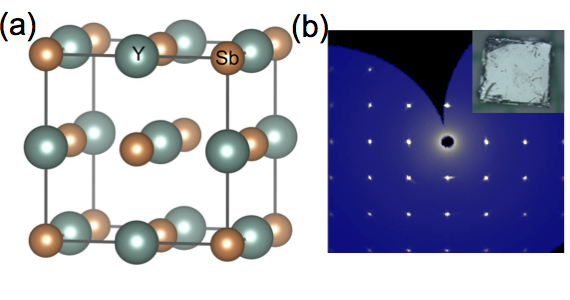
Single crystals of YSb were synthesized in Sb self flux. Y and Sb pieces were loaded in a 2 ml aluminum oxide crucible in a molar ratio of 1:15. The crucible was then sealed in a fused silica ampule under vacuum. The sealed ampoule was heated to 1175∘C over 10 hours, homogenized at 1175∘C for 12 hours and then cooled to 800∘C at the rate of 2∘C/hour. Once the furnace reached 800∘C, the excess flux was decanted from the crystals using a centrifuge. Well faceted cubic crystals as large as 3 mm 3 mm 3 mm were obtained. An optical image of a cleaved face of a 1.5 mm by 1.3 mm crystal is shown in the inset of Fig. 1(b).
The crystal structure of the compounds was verified by single crystal x-ray diffraction at room temperature using a STOE IPDS 2T diffractometer using Mo Kα radiation ( = 0.71073 ) and operating at 50 kV and 40 mA. Integration and numerical absorption corrections were performed using the X-AREA, X-RED, and X-SHAPE programs. Structures were solved by direct methods and refined by full-matrix least squares on F2 using the SHELXTL program package Shelxtl1997 .
Electrical resistivity measurements were made on an oriented crystal in a Quantum Design Physical Property Measurement System (PPMS) down to 1.8 K and in magnetic fields up to 9 T. A four wire configuration with 25 m gold wire and Epotek H20E silver epoxy were used for the resistivity and magnetoresistance measurements. The Hall effect was measured in a Hall bar geometry. Longitudinal (transverse) voltages were symmetrized (antisymmetrized) about H = 0 T, to account for the small misalignment of the voltage leads.
III Results and Discussion
The crystal structure of YSb determined from single crystal x-ray diffraction at room temperature is consistent with the NaCl type structure in cubic space group Fmm (# 225) as reported in literature abdusalyamova1990 . The crystallographic data are presented in Table 1. Y and Sb reside on the Wyckoff positions 4b and 4a, respectively. The atomic coordinates of Y are (1/2, 1/2, 1/2) and that of Sb are (0, 0, 0). The lattice parameter obtained from single crystal diffraction is a = 6.1652(7) Å. A sketch of the crystal structure of YSb is depicted in Fig. 1(a).
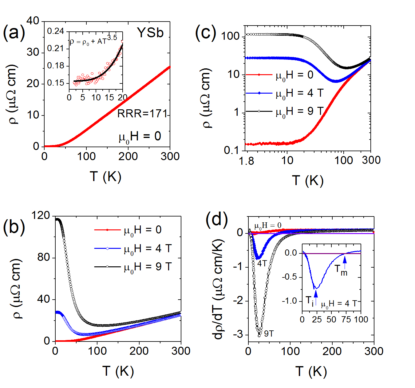
The zero field resistivity of YSb is shown in Fig. 2(a). The resistivity decreases with decreasing temperature from 300 to 13 K, consistent with a metallic behavior. However, the resistivity levels off below 13 K down to the lowest measured temperature (1.8 K). The residual resistivity ratio (RRR = (300 K)/(1.8 K) is 171, which reflects a high crystal quality. Below 20 K, the resistivity fits to (T, 0) = + ATn with = 0.1545(9) cm and n = 3.5(2), as shown in the inset of Fig. 2(a), a behavior similar to that of LaSb and LaBi Tafti2015 ; Sun2016 . Fig. 2(b) shows the temperature dependence of the resistivity of YSb measured in transverse magnetic fields of 0, 4 and 9 T applied along the c-axis. The effect of the magnetic field becomes significant at low temperatures. The resistivity starts to increase with decreasing temperature below 105 K at 9 T and below 70 K at 4 T. In all fields, the resistivity saturates below 13 K giving a pronounced resistivity plateau, reminiscent of the behavior of the topological insulators attributed to surface states. The low temperature behavior is shown more clearly in a log-log plot of vs in Fig. 2(c). The temperature derivative of the resistivity measured at 0, 4 and 9 T is depicted in Fig. 2(d). Similar to LaSb and LaBi Tafti2015 ; Sun2016 , a sharp peak is observed at 25 K in both fields, the temperature defined as the inflection point Ti. At higher temperature changes sign at Tm, which is magnetic field dependent: Tm at 4 and 9 T is 70 and 105 K, respectively.
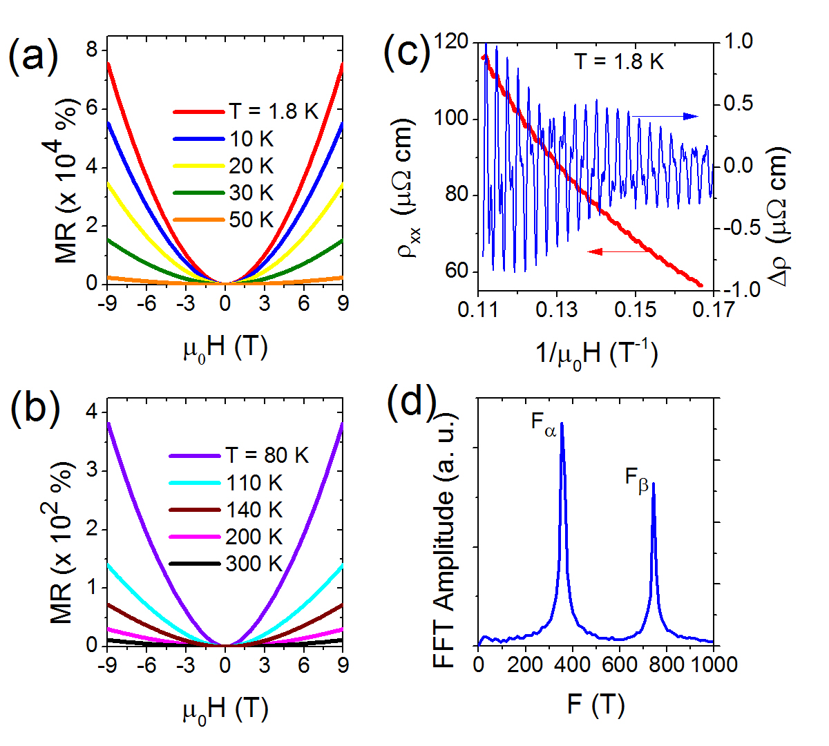
Transverse magnetoresistance, defined as MR = 100 [ - ]/ with H I, is presented in Fig. 3(a,b). At room temperature, there is a small MR of about 11 %. It increases rapidly with decreasing temperature and reaches over 75,000 % at 1.8 K and 9 T and remains unsaturated. This value compares to that of LaBi Sun2016 and is about an order of magnitude smaller than that reported for LaSb Tafti2015 ; Sun2016 . The magnetoresistance shows a quadratic behavior over the entire temperature range. In addition to the large MR, Shubnikov-de Haas (SdH) oscillations become clear at lower temperatures in the region of the resistivity plateau. The MR above 5 T measured at 1.8 K is shown by the red curve in Fig. 3(c). The SdH oscillations = - , obtained by subtracting a non-oscillatory background (a fourth order polynomial fit of ) from the oscillating , is plotted as the blue curve in Fig. 3(c). The frequencies of the quantum oscillations obtained by the Fast Fourier Transform (FFT) of as a function of 1/H is depicted in Fig. 3(d). Two fundamental frequencies of = 352 T and = 740 T are obtained. These frequencies are larger than in both LaSb and LaBi Tafti2015 ; Sun2016 suggesting a slightly larger Fermi surface in YSb than in the other two. This conclusion is supported by the first principles calculations presented below.
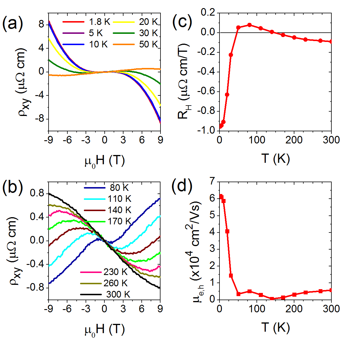
The Hall resistivity is defined as = (/), where is the thickness of the sample and is the transverse voltage in the presence of a magnetic field applied along -axis with current in the -plane. The Hall resistivity as a function of magnetic field at different temperatures is plotted in Fig. 4(a,b). At high temperatures, the sign of the Hall resistivity is opposite to that of the magnetic field, indicating electron-like carriers. This behavior changes with decreasing temperature, and becomes positive between 110 and 50 K, again becoming negative below 50 K, suggesting that the majority charge carriers change with temperature. A similar behavior is reported in LaSb Tafti2015 . The carrier concentration and Hall mobility can be analyzed within a single band model, which is most applicable at the lowest temperatures where the electron contribution dominates the Hall resistivity. The carrier concentration is given by = 1/(), where is the charge of the electron and is the Hall coefficient defined by = /(H). The temperature dependence of the Hall coefficient taken at 9 T is depicted in Fig. 4(c). The Hall mobility = 1/en is shown in Fig. 4(d). At 1.8 K, the computed carrier concentration is 6.5cm3, which is an upper bound since the hole contribution is not considered under the single band approximation. The Hall mobility at 1.8 K is 6.2 cm2/Vs. Again it is similar to LaBi Sun2016 and about an order of magnitude smaller than that of LaSb Tafti2015 .
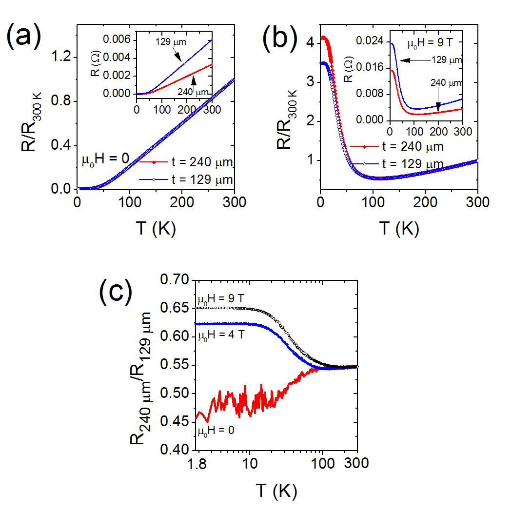
From Ohm’s law, the electrical resistance of a sample is given by R = , where is the resistivity of the material, is the length and is the cross-sectional area. If the thickness of a uniform metallic rectangular bar is decreased by a factor , the electrical resistance should increase by the same factor. We tested this for YSb. First, the electrical resistance of a 240 m thick sample was measured. Four gold stripes were made on a surface of the sample by gold sputtering to ensure the better contact between the gold wires and the sample. Gold wires were fixed on top of the stripes using silver epoxy (Epotek H20E). After the first measurement, the sample was polished on the back side to a thickness of 129 m. All four gold wires were kept intact. We found that for T 150 K the ratio of the resistance measured on the sample before and after polishing is equal to the ratio of the two thicknesses (=0.54) [Fig. 5(c)], which guarantees that the only change in the sample before and after polishing was its thickness. Figure 5(a) and 5(b) show the temperature dependence of normalized resistance R(T)/R(300 K) of the 240 and 129 m samples, measured in an external magnetic field of 0 and 9 T, respectively. The bare resistances are shown in the insets. The bare resistance of the thinner sample is larger both in 0 and 9 T over the entire temperature range. However, the normalized resistances of the two samples overlap at high temperature and change as the temperature decreases. A ratio of the resistance of 129 and 240 m samples (R129/R240) in 0, 4 and 9 T is depicted in Fig. 5(c). It is seen that this ratio is constant and equal to the ratio of the thickness above Tm. Below Tm, this ratio changes and again becomes constant below 13 K, where the resistivity plateau appears, indicating that in YSb the resistance does not scale to the inverse of the cross-sectional area as expected for a normal metal, irrespective of the presence of magnetic field. Deviation of such a scaling has also been observed in the topological Kondo insulator SmB6, Kim2014 where the behavior is attributed to a conducting surface state. In SmB6, the ratio of the resistance attains the value of unity providing evidence that the conduction occurs only on the surface. This ratio in YSb fails to reach unity even at the field of 9T, which suggests that the conduction channel in YSb up to 9 T is not solely through the surface. Interestingly, although the metal-insulator-like transition in YSb is induced by external magnetic field, the deviation of the scaling behavior is evident even in zero field [Fig. 5(c)].
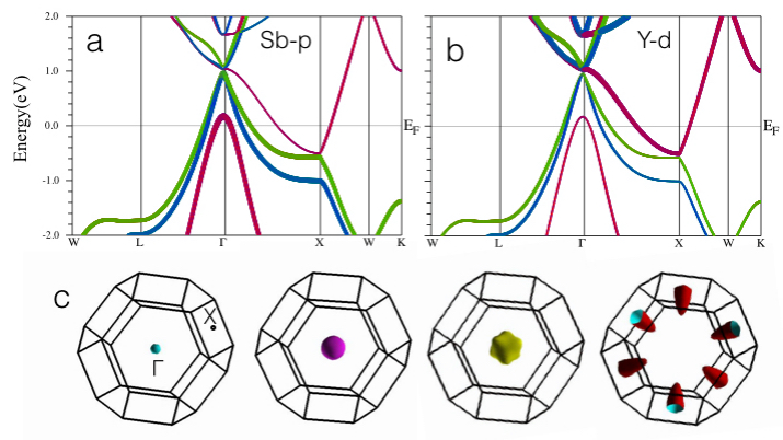
First principles calculations have been carried out to shed light into the striking similarity between the transport properties of YSb and those of LaSb and LaBi. The electronic structure calculations have been carried out within density functional theory (DFT) using the all-electron, full potential code WIEN2K wien2k based on the augmented plane wave plus local orbital (APW + lo) basis set APWlo . The Perdew-Burke-Ernzerhof (PBE) version of the generalized gradient approximation(GGA) GGA was chosen as the exchange correlation potential. Spin orbit coupling (SOC) was introduced in a second variational procedure SOC . A dense k-mesh of was used for the Brillouin Zone (BZ) sampling in order to check the fine details of the influence of spin orbit coupling in the electronic structure. A RmtKmax of 7.0 was chosen for all the calculations.
Figures 6(a, b) show the band structure with band character plot along high symmetry directions of the Brillouin zone with inclusion of SOC. The electronic structure corresponds to that of a compensated semimetal, with overlap of conduction and valence bands resembling that of LaSb and LaBi Gou2016 . The valence band has mainly Sb- character whereas the conduction band has primarily Y- character. The Fermi surfaces of YSb calculated with the inclusion of SOC are shown in Fig. 6(c). There are three nearly spherical hole pockets around the point with the equivalent ellipsoidal electron pockets centered at the X point. The electron and hole pockets have a larger volume in YSb as compared to LaSb and LaBi, and this is consistent with the experimental finding that the quantum oscillation frequencies are larger in YSb than in the other two compounds. Our calculations indicate that the resemblance in the transport properties of YSb and LaSb/LaBi stems from their similar electronic structures, which comprise compensating electron/hole carriers at the and X points of the Brillouin zone.
IV Conclusion
In summary, we have grown single crystals of YSb and studied its electrical transport properties. Overall, YSb behaves similarly to previously reported studies of LaSb and LaBi Tafti2015 ; Sun2016 . The magnetotransport displays a pronounced magnetoresistance, which does not saturate up to 9 T, with a large Hall mobility of 6.2 cm2/Vs at 1.8 K. The electronic structure of YSb corresponds to that of a compensated semimetal and is qualitatively similar to that of LaSb and LaBi. The results obtained from a thickness-dependent study indicate that the resistivity plateau observed at least up to 9 T cannot exclusively be attributed to surface conduction. The large magnetoresistance and the resistivity upturn in the external magnetic field below Tm have been attributed to the electron-hole compensation mechanism in LaBi Sun2016 and, possibly, in LaSb, Tafti2015 and YSb. It is interesting that the electrical resistance of YSb does not scale to the inverse of the thickness over the same temperature region. The centrosymmetric crystal lattice in this non-magnetic compound does not support the formation of the Fermi arc as in the Weyl semimetals. Likewise, quadratic behavior of the MR in all the measured temperatures is different from the linear MR behavior in Dirac semimetals Na3Bi and Cd3As2 Liang2015 ; Xiong2015 . Further investigation by, for example, Angle-Resolved Photoemission may shed further light on this issue. YSb provides an attractive system for such investigations because large single crystals with dimensions up to 3 mm are easily grown out of the Sb self flux, a consequence of the wide stability of YSb in an accessible temperature range - between 750 and 1200 ∘C in the Y-Sb phase diagram YSbPhasediagram1990 .
V Acknowledgements
This work was supported by the U.S. Department of Energy, Office of Science, Basic Energy Sciences, Materials Science and Engineering Division. The authors thank Duck Young Chung for his help during the crystal growth.
| Crystal system | Cubic |
|---|---|
| Space group | Fmm |
| Temperature (K) | 293(2) |
| Wavelength (Å) | 0.71073 |
| Z formula units | 4 |
| 2 | 5.73o |
| 2 | 28.38o |
| Formula weight (g/mol) | 210.66 |
| a (Å) | 6.1652(7) |
| Volume (Å3) | 234.34(8) |
| Density (calculated) (g/cm3) | 5.971 |
| (Mo K) (cm-1) | 357.09 |
| Goodness-of-fit on F2 | 1.144 |
| for | |
| 2 | 0.0147 |
| 0.0358 |
| Atom | Wyck. | Occ. | x | y | z | Ueq (Å2) |
|---|---|---|---|---|---|---|
| Y | 4b | 1 | 1/2 | 1/2 | 1/2 | 0.012(1) |
| Sb | 4a | 1 | 0 | 0 | 0 | 0.014(1) |
| = | = |
References
- (1) Hasan M Z and Kane C L 2010 Rev. Mod. Phys. 82 3045.
- (2) Hasan M Z, Xu S-Y and Bian G 2015 Phys. Scr. T164 014001.
- (3) Hasan M Z et. al. 2014 arXiv:1401.0848.
- (4) Yang B-J and Nagaosa N 2014 Nature Commun. 5 4898.
- (5) Ando Y 2013 J. Phys. Soc. Jpn. 82 102001.
- (6) Qi X-I and Zhang S-C 2011 Rev. Mod. Phys 83 1057.
- (7) Dzero M et. al. 2010 Phys. Rev. Lett. 104 106408.
- (8) Moore J E 2010 Nature 464 194.
- (9) Xu S-Y et. al. 2015 Science 347 294.
- (10) Young S-M et. al. 2012 Phys. Rev. Lett. 108 140405.
- (11) Xu S-Y et. al. 2015 Science 349 613.
- (12) Kim D J, Xia J and Fisk Z 2014 Nature Mater. 13 466.
- (13) Ren Z et. al. 2010 Phys. Rev. B 82 241306.
- (14) Kim K J et. al. 2013 Sci. Rep. 3 3150.
- (15) Huang S-M et. al. 2015 Nature Commun. 6 7373.
- (16) Lv B Q et. al. 2015 Nature Phys. 11 724.
- (17) Borisenko S et. al. 2014 Phys. Rev. Lett 113 027603.
- (18) Huang X et. al. 2015 Phys. Rev. X 031023.
- (19) Shekhar C et. al. 2015 Nature Phys. 11 645.
- (20) Ghimire N J et. al. 2015 J. Phys.: Condens. Mater. 27 152201.
- (21) Tafti F F et. al. 2015 Nature Phys. doi:10.1038/nphys3581.
- (22) Sun S et. al. 2016 arXiv:1601.04618.
- (23) Kumar N et. al. 2016 arXiv:1601.07494.
- (24) Wang K et. al. 2014 Sci. Rep. 4 7328.
- (25) Luo Y et. al. 2016 arXiv:1601.05524.
- (26) Li Y et. al. 2016 arXiv:1601.02062.
- (27) Wu D et. al. 2016 Appl. Phys. Lett. 108 042105.
- (28) Ali M N et. al. 2014 Nature 514 205.
- (29) Liang T et. al. 2015 Nature Mater. 14 280.
- (30) Xiong J et. al. 2015 arXiv:1502.06266.
- (31) SHELXTL 1997 “SJE:XTL program package,” SHELXTL 5.10 1997 Bruker AXS, Inc., Madison, Wisconsin 53719.
- (32) Abdusalyamova M N et. al. J. Less Common Met. 166 227.
- (33) Blaha P, Schwarz K, Madsen G K H et al. 2001 WIEN2K, An Augmented Plane Wave Plus Local Orbitals Program for Calculating Crystal Properties (Vienna University of Technology, Austria).
- (34) Sjostedt E, Nordström L, and D. Singh 2000 Solid State Commun 114 15.
- (35) Perdew J P, Burke K, and Ernzerhof M 1996 Phys. Rev. Lett. 77 3865.
- (36) Singh D, and Nordström L 2006 Plane Waves, Pseudopotentials and LAPW Method (New York: Springer).
- (37) Guo P-J, Yang H-C, Liu K and Lu Z-Y arXiv:1602.05061.
- (38) Okamoto H 1990 “Sb-Y (Antimony-Yttirium),” Binary Alloy Phase Diagrams 3 3317.