Charge ordering in Ni1+/Ni2+ nickelates: La4Ni3O8 and La3Ni2O6
Abstract
Ab initio calculations allow us to establish a close connection between the Ruddlesden-Popper layered nickelates and cuprates not only in terms of filling of -levels (close to ) but also because they show Ni1+(S=1/2)/Ni2+(S=0) stripe ordering. The insulating charge ordered ground state is obtained from a combination of structural distortions and magnetic order. The Ni2+ ions are in a low-spin configuration (S=0) yielding an antiferromagnetic arrangement of Ni1+ S=1/2 ions like the long-sought spin-1/2 antiferromagnetic insulator analog of the cuprate parent materials. The analogy extends further with the main contribution to the bands near the Fermi energy coming from hybridized Ni-d and O- states.
pacs:
71.20.-b, 75.47.Lx, 74.72.-hLayered nickelates have been regarded as the best analog of high temperature superconducting cuprates if the Ni1+ state can be stabilized in analogy to Cu2+ Hansmann et al. (2009). The discovery of the Ruddlesden-Popper phases Lnn-1(NiO2)nLn2O2 (Ln=La, Pr, Nd; n=1, 2, 3) with cuprate-like NiO2 layers reinvigorated the interest in nickelates Greenblatt (1997); Zhang et al. (1994); Greenblatt et al. (1997); Poltavets et al. (2006, 2007, 2009, 2010); Zhang et al. (2016). Within this series, the trilayer La4Ni3O8 (La438) and bilayer La3Ni2O6 (La326) compounds are ionic but highly unconventional insulators Poltavets et al. (2009, 2010). As the =3 and =2 members of the series, they have a formal Ni valence of +1.33 and +1.5, respectively, which being non-integer should correspond to metallic behavior, yet both are insulating. The NiO2 slabs are separated by fluorite structure LaO blocking layers that make the inter-trilayer/bilayer coupling very weak. The lack of apical oxygen ions reduces the interplane separation substantially and opens a large crystal field splitting for the states with the d state lying higher in energy than d. The d orbitals hybridize along the direction giving rise to molecular subbands. Depending on the relative magnitude of the crystal field splitting and Hund’s rule coupling, the ground state can be either high spin (HS) and insulating or low spin (LS) and metallic as depicted in Fig. 1.
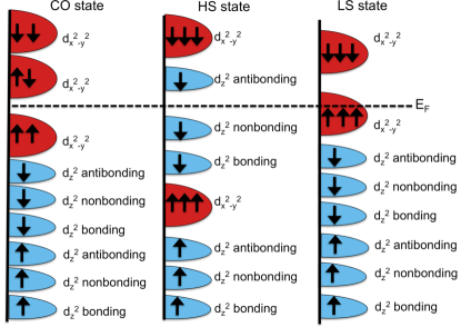
The =3 La438 compound undergoes a phase transition to an insulating state at 105 K, accompanied by a dramatic increase in the resistivity and a discontinuity in the magnetization Poltavets et al. (2010); Zhang et al. (2016). NMR experiments reveal the presence of spin fluctuations below 160 K Aproberts-Warren et al. (2011). From a theoretical point of view, the insulating character of La438 was accounted for in terms of a molecular high spin (HS) state with the insulator-to-metal transition being spin driven Pardo and Pickett (2010, 2011, 2012). With the gap being formed between d bands, the electronic structure of the high spin state differs from the one in cuprates.
Although the trilayer nickelate exhibits a transition likely accompanied by antiferromagnetic (AFM) order, the insulating bilayer material shows no transition down to 4 K Poltavets et al. (2009). Transport and magnetic measurements have shown that La326 is a paramagnetic insulator with spin fluctuations similar to those seen in La438 apRoberts-Warren et al. (2013). The crystal field splitting, Hund’s rule coupling, and ostensibly the AFM exchange interactions should be comparable to those in the trilayer material. The different electron count (and Ni average valence) leads to the presence of two versus three d orbitals forming the molecular basis. Generally viewed, the physics of the spin states and possibilities for an insulating molecular state are quite similar in La326 and La438, though the different energy scales are such that the former has not shown a transition yet in the temperature range studied Poltavets et al. (2009); apRoberts-Warren et al. (2013).
Recently, Zhang et al. Zhang et al. (2016) showed using x-ray diffraction on single crystals of La438 that the transition is associated with real space ordering of charge within each plane forming a striped ground state. The superlattice propagation vector is oriented at 45∘ to the Ni-O bonds with the stripes being weakly correlated along to form a staggered AB stacking of the trilayers. Within each trilayer, the stripes are stacked in phase from one layer to the next. This planar charge modulation provides an alternate route to the insulating state as compared to the previous picture based on molecular orbitals formed by hybridization along .
Here, using density functional theory (DFT)-based calculations, we show that a charge ordered phase of Ni1+ (S=1/2)/Ni2+(S=0) stripes has a lower free energy than the previously suggested molecular insulating state in La438, and this accounts for both the insulating nature and the superlattic peaks seen experimentally. The gap opens up from a combination of charge-ordered related structural distortions and exchange splitting and is formed solely within the d manifold of states. When doped, electrons or holes would go into these states, in a similar fashion to what occurs in the cuprates. Analogous calculations suggest that checkerboard charge order should appear in the bilayer nickelate La3Ni2O6. Confirmation would ideally require single crystals of La326, which are challenging to synthesize, as well as studies at higher temperatures to access the transition itself.
DFT calculations were performed using the all-electron, full potential code WIEN2K Blaha et al. (2001) based on an augmented plane wave plus local orbital (APW+lo) basis set Sjöstedt et al. (2000), with atomic positions taken from a recent crystal structure refinement Zhang et al. (2016). For the structural relaxations, we have used the Perdew-Burke-Ernzerhof version of the generalized gradient approximation (GGA) Perdew et al. (1996).
Our charge-ordered ground state configuration for La438 is found even in the absence of an on-site Coulomb repulsion and Hund’s rule coupling strength JH. But, to compute more reliably the total energy difference between the 2D striped phase and the 3D molecular insulating state, the LDA+ scheme has been applied using the so-called fully localized version for the double-counting correction Lichtenstein et al. (1995); Petukhov et al. (2003) that incorporates a and JH for the Ni states. Chosen values for and are 4.75 and 0.68 eV, respectively, as used in earlier work Pardo and Pickett (2010). Calculations confirm that a 2D charge ordered state is more stable than the previously proposed HS state by 0.4 eV/Ni within LDA+, so large that the particular choice of is not critical.
Charge ordering in La438. In La438, the average formal Ni valence is +1.33. One possibility would be an in-trimer charge-ordered configuration with the outer Ni atoms being Ni1+ and the inner Ni2+ but this has been shown to be very unfavorable in energy Wu (2013). If all the Ni ions have the same valence, the eg states, with 2.67 electrons per Ni on average can occur in two different ways: the LS state and the HS state that give rise to a metallic and an insulating state, respectively (Fig. 1) Pardo and Pickett (2010). These have been the possibilities explored so far, without accounting for any potential in-plane charge ordering that we explore here.
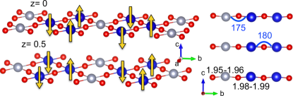
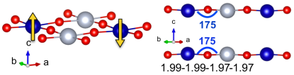
To test the possibility of 2D charge ordering, a 3 supercell was used with the charge/spin pattern shown in Fig. 2. Formal Ni1+:d9 (S=1/2) and Ni2+:d8 (S=0) ions in a 2:1 ratio form stripes at 45∘ to the Ni-O bonds with the Ni1+ stripes coupled antiferromagnetically. Such type of charge and spin ordering yields an AFM arrangement of Ni1+ S= ions analog of the cuprate parent materials. Note that the imposed stacking of trilayers is AA and not the experimental AB one since that would require larger supercells. In either case, the coupling between trilayers is weak and within each trilayer the stripes are stacked in phase.
The structure has been relaxed with the lattice constants fixed to the experimental values, so only internal atomic positions were optimized. There is a significant distortion of the Ni-O distances in the NiO2 planes consisting of a modulation of the Ni-O bond length: shorter around the Ni2+ ions (1.95-1.96 Å) and longer around the Ni1+ ions (1.98-1.99 Å) keeping the average distance very similar to the experimentally reported value. Also, as shown in Fig. 2, there is significant buckling of the outer NiO2 planes with the inner plane remaining flat. The Ni-Ni distance (both in plane and out of plane) remains unaltered after the relaxation (3.96 Å in plane, 3.25 Å out of plane) given the fixed lattice constants.
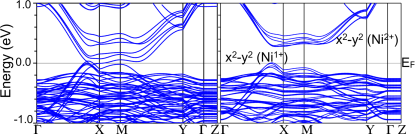
Charge order-related structural distortions are responsible for the opening of a gap and the corresponding stabilization of the striped phase. Without distortions, a gap cannot be opened up to the highest value reached in our calculations of 6 eV. Figure 3 shows the band structure for the unrelaxed structure (metallic, on the left) and for the distorted structure after relaxation (insulating, on the right). The insulating character of the derived distorted structure can be observed with a gap of 0.25 eV that opens up near even without introducing a Coulomb . For a = 4.75 eV the gap increases to only 0.6 eV.
As in cuprates, the gap is of d-only character. From the simple ionic picture, the Ni2+ d8 (S=0) cations have two empty d bands. The Ni1+ d9 (S=1/2) ions have one hole in the minority-spin d band, with the gap being formed between occupied and unoccupied d states. Since the Hund’s rule coupling is larger than the bandwidth, the introduction of is not necessary to open a gap.
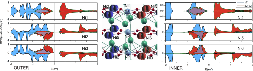
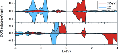
To further analyze the electronic structure, Fig. 4 shows the calculated orbital resolved density of states (DOS) of the different Ni atoms. In the striped phase, the Ni2+ (d8 LS, S=0) ions have all the bands (majority and minority spin) occupied with the wide d band for both spin channels remaining unoccupied. For the Ni1+ (d9, S=1/2) ions, the d states are also fully occupied and the d of the minority spin channel is unoccupied. The DOS clearly shows how the gap is formed between d bands with predominantly Ni1+ character at the top of the valence band and d bands with predominantly Ni2+ character at the bottom of the conduction band. The spin density, pictured in Fig. 4, also reveals d-only character. The analogy with cuprates extends further since there is a high degree of hybridization between Ni-d and O- states in the vicinity of the Fermi level. This contrasts with the previously proposed insulating HS state where only d states lie close to the Fermi level and O- bands are at much lower energies, around 2 eV below the Fermi energy (see Fig. 1 in the Supplementary Material).
Since the discovery of stripe order in high Tc layered cuprates Tranquada et al. (1995); Anisimov et al. (2004), spin/charge ordering has attracted considerable interest. Our results suggest that the underlying physics of stripe phases in nickelates and cuprates is intimately related in terms of pure electron count and because the stripe ordering of charges and magnetic moments involves bands of d-only character that are highly hybridized with O- states. Let us recall that similar stripe ordering has been observed and well studied in single layer nickelates, i.e. La2-xSrxNiO4 (LSNO) Hayden et al. (1992); Cheong et al. (1994); Ikeda et al. (2015). However, they are further from cuprates in terms of electron count (between d7 and d8), spin state, and due to the role that d orbitals play in the vicinity of the Fermi level.
The calculated magnetic moments confirm the formal charge states we have quoted. For the Ni1+ ions, the magnetic moments inside the muffin-tin sphere are 0.6-0.7 . For Ni2+, the moment is zero. To assess the physical Ni charge distributions, the decomposed radial charge densities inside Ni1+ and Ni2+ spheres were compared directly. The occupations, obtained from the maximum in the radial charge density plots, are identical for Ni2+ and Ni1+. The majority and minority spin valence radial charge densities do differ as they must to give the moment, but the total occupation does not differ (see Fig. 2 in the Supplementary Material). This invariance of the actual electron occupation (i.e., the charge) in many charge-ordered oxide systems has been discussed in the past Quan and Pickett (2015); Quan et al. (2012). The formal charge of a cation involves the environment of the cation, including the distance to neighboring oxygen ions and the Madelung potentials from the structure (note that the energy difference of the Ni-2 core levels for Ni1+ and Ni2+ ions is 0.2 eV). Remarkably, despite the almost equal charge of the two types of Ni atoms, the band structure has a pronounced ionic character reflective of 1+ and 2+ valences.
Charge ordering in La326. The similarities between La438 and La326 led us to study the possibility of charge ordering in the =2 compound, with an average formal Ni valence +1.5. We predict a closely related checkerboard charge ordered insulating phase for La3Ni2O6 that provides a 2D AFM spin-half insulator based on Ni1+ (see Fig. 5). The checkerboard phase is more stable than the previously proposed HS state by 0.7 eV/Ni within LDA+ (= 4.75 eV) (again a large energy difference). The structural relaxations within GGA for this magnetic order share the main features with those for La438: a shorter Ni-O bond length for Ni2+ atoms (1.97 Å) and a longer one around the Ni1+ ones (1.99 Å), as well as significant buckling of the NiO2 plane. The magnetic moments obtained are consistent with the Ni2+-Ni1+ charge ordering picture. For the Ni1+ ions, the magnetic moments inside the muffin-tin sphere are 0.7 . For Ni2+, the moment is zero.
In the case of La326, the introduction of a is needed to open a gap in the charge ordered state. Within GGA, the d bands are wider (W2 eV) than for La438. With the gap being formed only between d states in the charge ordered state, if the Hund’s rule coupling is smaller than the bandwidth, a is needed to obtain an insulating solution. The corresponding orbital resolved density of states for Ni1+ and Ni2+ in La326 is shown in Fig. 6. A decoupling of the states is clear: the bands are either Ni1+ or Ni2+ with negligible mixing and a gap of 0.55 eV. Both Ni sites have all states occupied with the relatively broad Ni2+ d states unoccupied. The Ni1+ ions have d orbitals split into upper and lower Hubbard bands by the Hubbard , providing a moment near that expected for S=. As in La438, the gap is between occupied Ni1+-d and unoccupied Ni2+-d states.
To summarize, ab initio calculations give rise to a 2D AFM spin-half insulating ground state based on Ni1+ (pseudo Cu2+) stripes for Ruddlesden-Popper layered nickelates. The gap opens from a combination of charge ordered related structural distortions and magnetic order for both La4Ni3O8 and La3Ni2O6. Our results show a similar electronic structure of these layered nickelates to cuprates not only by pure electron count (close to a d9 configuration), but also because the bands involved around the Fermi level are of of character only. These results bring renewed justification that layered nickelates of this type are the cuprate analog systems that are promising for studying the interplay between structure, magnetism, and possibly superconductivity.
We thank John Mitchell, Junjie Zhang, and Daniel Khomskii for stimulating discussions. Work at Argonne was supported by the Materials Sciences and Engineering Division, Basic Energy Sciences, Office of Science, US DOE. V.P. thanks MINECO for project MAT2013-44673-R, the Xunta de Galicia through project EM2013/037, and the Spanish Government through the Ramon y Cajal Program (RYC-2011-09024). W.E.P. was supported by Department of Energy Grant No. DE-FG02-04ER46111.
References
- Hansmann et al. (2009) P. Hansmann, X. Yang, A. Toschi, G. Khaliullin, O. K. Andersen, and K. Held, Phys. Rev. Lett. 103, 016401 (2009).
- Greenblatt (1997) M. Greenblatt, Curr. Opin. Solid State Mater. Sci. 2, 174 (1997).
- Zhang et al. (1994) Z. Zhang, M. Greenblatt, and J. Goodenough, J. Solid State Chem. 108, 402 (1994).
- Greenblatt et al. (1997) M. G. Greenblatt, Z. Zhang, and M. H. Whangbo, Synth. Met. 85, 1451 (1997).
- Poltavets et al. (2006) V. V. Poltavets, K. A. Lokshin, S. Dikmen, M. Croft, T. Egami, and M. Greenblatt, J. Am. Chem. Soc. 128, 9050 (2006).
- Poltavets et al. (2007) V. V. Poltavets, K. A. Lokshin, M. Croft, T. K. Mandal, T. Egami, and M. Greenblatt, Inorg. Chem. 46, 10887 (2007).
- Poltavets et al. (2009) V. V. Poltavets, M. Greenblatt, G. H. Fecher, and C. Felser, Phys. Rev. Lett. 102, 046405 (2009).
- Poltavets et al. (2010) V. V. Poltavets, K. A. Lokshin, A. H. Nevidomskyy, M. Croft, T. A. Tyson, J. Hadermann, G. Van Tendeloo, T. Egami, G. Kotliar, N. Aproberts-Warren, et al., Phys. Rev. Lett. 104, 206403 (2010).
- Zhang et al. (2016) J. Zhang, Y. S Chen, D. Phelan, H. Zheng, M. R. Norman, and J. F. Mitchell, arxiv 1601.03711 (2016).
- Aproberts-Warren et al. (2011) N. Aproberts-Warren, A. P. Dioguardi, V. V. Poltavets, M. Greenblatt, P. Klavins, and N. J. Curro, Phys. Rev. B 83, 014402 (2011).
- Pardo and Pickett (2010) V. Pardo and W. E. Pickett, Phys. Rev. Lett. 105, 266402 (2010).
- Pardo and Pickett (2011) V. Pardo and W. E. Pickett, Phys. Rev. B 83, 245128 (2011).
- Pardo and Pickett (2012) V. Pardo and W. E. Pickett, Phys. Rev. B 85, 045111 (2012).
- apRoberts-Warren et al. (2013) N. apRoberts-Warren, J. Crocker, A. P. Dioguardi, K. R. Shirer, V. V. Poltavets, M. Greenblatt, P. Klavins, and N. J. Curro, Phys. Rev. B 88, 075124 (2013).
- Blaha et al. (2001) P. Blaha, K. Schwarz, G. K. H. Madsen, D. Kvasnicka, and J. Luitz, WIEN2k, An Augmented Plane Wave Plus Local Orbitals Program for Calculating Crystal Properties, Vienna University of Technology, Austria (2001).
- Sjöstedt et al. (2000) E. Sjöstedt, L. Nördstrom, and D. Singh, Solid State Commun. 114, 15 (2000).
- Perdew et al. (1996) J. P. Perdew, K. Burke, and M. Ernzerhof, Phys. Rev. Lett. 77, 3865 (1996).
- Lichtenstein et al. (1995) A. I. Liechtenstein, V. I. Anisimov, and J. Zaanen, Phys. Rev. B 52, R5467 (1995).
- Petukhov et al. (2003) A. G. Petukhov, I. I. Mazin, L. Chioncel, and A. I. Lichtenstein, Phys. Rev. B 67, 153106 (2003).
- Wu (2013) H. Wu, New J. Phys. 15, 023038 (2013).
- Kokalj (2003) A. Kokalj, Computational Materials Science 28, 155 (2003).
- Quan and Pickett (2015) Y. Quan and W. E. Pickett, Phys. Rev. B 91, 035121 (2015).
- Quan et al. (2012) Y. Quan, V. Pardo, and W. E. Pickett, Phys. Rev. Lett. 109, 216401 (2012).
- Tranquada et al. (1995) J. M. Tranquada, B. J. Sternlieb, J. D. Axe, Y. Nakamura, and S. Uchida, Nature 375, 561 (1995).
- Anisimov et al. (2004) V. I. Anisimov, M. A. Korotin, A. S. Mylnikova, A. V. Kozhevnikov, D. M. Korotin, and J. Lorenzana, Phys. Rev. B 70, 172501 (2004).
- Hayden et al. (1992) S. M. Hayden, G. H. Lander, J. Zarestky, P. J. Brown, C. Stassis, P. Metcalf, and J. M. Honig, Phys. Rev. Lett. 68, 1061 (1992).
- Cheong et al. (1994) S.-W. Cheong, H. Y. Hwang, C. H. Chen, B. Batlogg, L. W. Rupp, and S. A. Carter, Phys. Rev. B 49, 7088 (1994).
- Ikeda et al. (2015) Y. Ikeda, S. Suzuki, T. Nakabayashi, H. Yoshizawa, T. Yokoo, and S. Itoh, J. Phys. Soc. Jpn 84, 023706 (2015).