Control of valley dynamics in silicon quantum dots in the presence of an interface step
Abstract
Recent experiments on silicon nanostructures have seen breakthroughs toward scalable, long-lived quantum information processing. The valley degree of freedom plays a fundamental role in these devices, and the two lowest-energy electronic states of a silicon quantum dot can form a valley qubit. In this work, we show that a single-atom high step at the silicon/barrier interface induces a strong interaction of the qubit and in-plane electric fields, and analyze the consequences of this enhanced interaction on the dynamics of the qubit. The charge densities of the qubit states are deformed differently by the interface step, allowing non-demolition qubit readout via valley-to-charge conversion. A gate-induced in-plane electric field together with the interface step enables fast control of the valley qubit via electrically driven valley resonance. We calculate single- and two-qubit gate times, as well as relaxation and dephasing times, and present predictions for the parameter range where the gate times can be much shorter than the relaxation time and dephasing is reduced.
I Introduction
Localized spins in silicon quantum dot (QD) and donor systems are actively investigated as platforms for quantum computing Kane (1998); Zwanenburg et al. (2013). The chief reason for this is their long spin coherence times Feher (1959); Feher and Gere (1959); Roth (1960); Hasegawa (1960); Simmons et al. (2011); Raith et al. (2011); Tahan and Joynt (2014); Bermeister et al. (2014); Kha et al. (2015) due to weak spin-orbit coupling, the existence of nuclear-spin free isotopes allowing isotopic purification Itoh and Watanabe (ions), and the absence of piezoelectric electron-phonon coupling Yu and Cardona (2010). Recent years have witnessed enormous experimental strides towards making silicon quantum computing scalable and long-lived Morello et al. (2010); Tracy et al. (2010); Pla et al. (2012, 2013); Veldhorst et al. (2014), with long spin coherence times observed for single electrons, Muhonen et al. (2014) as well as demonstrations of electrical spin control Kawakami et al. (2014) and entanglement Veldhorst et al. (2015a); Weber et al. (2014).
The valley degree of freedom has emerged as an important ingredient of silicon quantum bits (qubits). It increases the size of the qubit Hilbert space and introduces fundamental complications in particular in entanglement, such as exchange oscillations in donors and suppression in QDs Cullis and Marko (1970); Koiller et al. (2001); Boykin et al. (2004); Wellard and Hollenberg (2005); Friesen et al. (2007); Culcer et al. (2010); Friesen and Coppersmith (2010). For example, valley interference effects have recently been experimentally observed in donors Salfi et al. (2014). In addition, intervalley spin-orbit coupling terms can induce simultaneous spin-valley dynamics, affecting spin relaxation as well as the -factor of QDs Kawakami et al. (2014); Nestoklon et al. (2006); Li and Dery (2011); Huang and Hu (2014); Veldhorst et al. (2015b). Interestingly, the valley splitting can be measured and the valley degree of freedom can be controlled by a means of a gate-induced out-of-plane electric field Saraiva et al. (2011); Lim et al. (2011); Wu and Culcer (2012); Culcer et al. (2012); Yang et al. (2013); Kim et al. (2014); Hao et al. (2014). This realization has led to the proposal of a two-electron qubit encoded in the valley degree of freedom itself Culcer et al. (2012), which is expected to have good coherence properties Tahan and Joynt (2014). Quantum control and coherence properties of valley qubits and combined spin-valley qubits are also being explored actively in a range of other materials, including grapheneRecher et al. (2007), carbon nanotubesPályi and Burkard (2011); Laird et al. (2013); Széchenyi and Pályi (2014); Laird et al. (2015), and transition metal dicalcogenidesKormányos et al. (2014); Wu et al. (2016).
In this work, we theoretically study the dynamics of a single-electron valley qubit in a silicon QD. The valley qubit is formed by the two lowest-energy electronic states of the QD. We demonstrate that a single-atom high step at the silicon/barrier interface (see Fig. 1), a defect ubiquitous in silicon nanostructures, can induce a strong interaction of the qubit and in-plane electric fields. We show that the charge densities of the two qubit states are deformed differently by the interface step, as the relative position of the QD and the edge of the interface step is tuned by a gate-induced in-plane electric field. This provides an opportunity for non-demolition qubit readout via valley-to-charge conversion. Furthermore, we demonstrate that, in the vicinity of the step, the physics of the valley qubit is analogous to that of a charge qubit in a double quantum dot.
Our main goal then is to discuss and quantify the coherent-control opportunities and the decoherence mechanisms arising from the enhanced interaction between the qubit and the in-plane electric fields. We determine the relaxation and dephasing matrix elements characterizing this interaction. We discuss the role of the relaxation matrix element in enabling fast single-qubit control via electrically driven valley resonance as well as entanglement via an two-qubit gate. Concomitantly, we study qubit relaxation via spontaneous phonon emission and show that, although valley relaxation times can range over several orders of magnitude, in certain parameter regimes the single-qubit gate times can be much shorter than the relaxation time, allowing approximately operations in one relaxation time. Finally, we discuss qubit dephasing rates due to background charge fluctuations and identify an operational window in which dephasing is reduced.
We model the system based on the hybrid approach of Ref. Gamble et al., 2013, using the effective mass approximation to describe the dynamics in the plane of the interface and a tight-binding approximation for the dynamics perpendicular to the interface. Our setup does not include a magnetic field and we do not consider explicitly the spin degree of freedom.
The outline of this paper is as follows. In Sec. II we introduce the physical setup considered in this work and the model Hamiltonian used to study it, while in Sec. III we discuss in detail valley-to-charge conversion. Sec. IV is devoted to the dynamics of the valley qubit, comprising coherent control due to an external electric field as well as relaxation due to phonons and dephasing due to charge noise. We summarize our findings in Sec. V.
II Setup and model
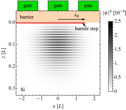
We consider a single conduction-band electron in a gate-defined QD at a silicon/barrier interface. The setup, along with the spatial dependence of the ground-state particle density of the electron, is shown in Fig. 1. The colored regions represent the barrier material (e.g., SiGe or SiO2), and the region below represents silicon. The axis is aligned with the [001] crystallographic direction of silicon. The in-plane confinement potential for the electron is created by top gates. The gate-induced electric field pushes the electron against the barrier, and also defines the lateral confinement parallel to the plane. The key element of the setup is a single-atom high barrier step at the silicon/barrier interface, depicted as the red (dark gray) stripe. The step consists of the atoms of the barrier material, is assumed to be translationally invariant along y, and the relative position of the step edge and the center of the lateral confinement potential is denoted by .
Note that the setup considered here, incorporating a half-infinite barrier step at the silicon/barrier interface, is similar to the one considered in Ref. Gamble et al., 2013. (The model used in Ref. Gamble et al., 2013 is also adopted here, see below.) Therein, the authors describe a single-atom high barrier step that has a rectangular shape in the plane, with a fixed location with respect to the lateral confinement potential, and compute and discuss how the energy levels and the dephasing matrix elements (see below for definitions) depend on the gate-induced -directional electric field that pushes the electron toward the upper barrier. Inspired by that study, here we address the following distinct questions: (i) How do the wave functions behave as the relative position of the step and the QD is varied, for example, under the action of an in-plane electric field? (ii) What is the reason for the observed behavior? (iii) What are the qualitative and quantitative consequences of the observed behavior in the context of coherent control and information loss of the valley qubit?
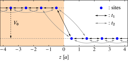
We describe the electron using the hybrid model introduced in Ref. Gamble et al., 2013, which combines the envelope-function approximation to treat the wave function in the plane, with a one-dimensional tight-binding modelBoykin et al. (2004) (chain) along the axis. That distinction between the plane and the direction is made to account for the fact that the electronic wave function in a silicon quantum dot is a packet of Bloch waves that reside in the and valleys of silicon’s conduction band. As a consequence, in this hybrid model, the electronic wave function has two continuous spatial variables, the and coordinates, and one integer spatial variable, the site index along the chain. Here, the integer is associated to the position of the th site of the chain, and is the lattice constant of the latter. We use the normalization relation , where is the lateral confinement length defined below. Of course, the spatial structure of the Hamiltonian is analogous to that of the wave function.
In the chain along , depicted in Fig. 2, the neighboring sites represent neighboring atomic layers of silicon, therefore is chosen, with being the lattice constant of silicon. Note also that we neglect the spin degree of freedom from now on.
The electron in the QD is confined by the gate-induced electric fields and by the barrier material. These effects are taken into account as electrostatic potentials:
| (1a) | |||||
| (1b) | |||||
| (1c) | |||||
| (1d) | |||||
Here, represents the interface electric field pushing the electron against the barrier, represents the gate-induced lateral confinement potential, and represents the conduction-band offset of the barrier material (). The function specifies the spatial range of the barrier material: , , and , where is the Heaviside function. Furthermore, is the transverse effective mass of the silicon conduction band. We also introduce the lateral confinement length .
The complete Hamiltonian also incorporates the kinetic energy term :
| (2) |
Here, the kinetic energy associated to electron hopping between atomic layers along the direction:
| (3) |
where () is the nearest-neighbor (next-nearest-neighbor) hopping amplitude. These values are setBoykin et al. (2004) so that the corresponding one-dimensional bulk dispersion relation reproduces the longitudinal effective mass of the conduction-band bottom as well as the momentum component corresponding to the and valleys of silicon’s conduction band.
In what follows, we focus on the properties of the lowest two energy eigenstates of the QD, and , which are computed numerically by diagonalizing the complete Hamiltonian . We set , representing SiGe as the barrier material. The results presented here were obtained using an interface electric field of , and a lateral confinement energy , corresponding to a lateral confinement length . Further details of the model and the numerical implementation are in Appendix A.
III Valley-to-charge conversion
We consider the two-level system formed by the two lowest-energy eigenstates, and , of the Hamiltonian . We refer to this system as the valley qubit, and to the two energy eigenstates as the valley-qubit basis states. If the QD is located on a flat silicon/barrier interface, then the gross spatial features of the charge densities of the two valley-qubit basis states are very similar (see, e.g., Fig. 3c, leftmost column), indistinguishable for a usual charge sensor that lacks atomic spatial resolution. In this section, we argue that a single-atom high interface step can be utilized to bring the valley qubit to a state where it resembles a conventional charge qubit in a double quantum dot. We refer to this phenomenon as valley-to-charge conversion. Therefore, in principle, such a setup allows for a projective non-demolition readout of the valley qubit via charge sensing. Furthermore, in the next section we quantify how this valley-to-charge conversion strengthens the interaction of the valley qubit with electric fields, and, in turn, how it enhances the effectivity of coherent-control operations as well as decoherence mechanisms.
Let us start by introducing the key parameter , which we refer to as the step edge position. In the considered setup, see Fig. 1, we identify the origin of the axis with the center of the lateral confinement potential. The step edge position is defined as the distance between the center of the lateral confinement potential and the step edge. We envision the possibility that is in situ tuneable: a sufficiently sophisticated top-gate electrode structure could be utilized to control by moving the lateral QD confinement potential and hence the electron itself along the axis.
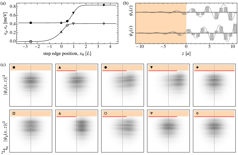
The opportunity for valley-to-charge conversion is suggested by the dependence of the wave functions of and , in the absence of the stepFriesen et al. (2007); Tahan and Joynt (2014). In this case, the wave function is a product of -, - and -dependent factors; the dependence of and on is shown in Fig. 3b (cf. Fig. 8 of Ref. Tahan and Joynt, 2014). The key observations are as follows. (i) The ground state has a nearly vanishing wave function at the last atomic layer of the barrier material (), and it has a peak in the first silicon layer (). (ii) The wave function of the excited state is peaked at the last barrier layer but is close to zero at the first silicon layer. A simple interpretation of these two observations is given in Appendix B.
As a consequence of (i), we expect that if the electron occupies , and we try to move it above the step, then it will resist to move together with the lateral confinement potential, as it has an appreciable probability of being in the atomic layer of the step. However, as a consequence of (ii), if the electron occupies , then it can follow the lateral confinement potential as its probability of occupying the layer of the atomic step almost vanishes.
To confirm these expectations, we computed the wave functions of the energy eigenstates and . The corresponding particle densities in the plane are shown in Fig. 3c, for five selected values of the step edge position , see Fig. 3a, confirming our expectations about valley-to-charge conversion. The subplots and of Fig. 3c show the ground-state and excited-state particle densities when the electron is confined far from the step, . As an attempt is made to move the electron on the step by the gates, that is, the lateral confinement potential is moved such that (subplot and in Fig. 3c), the ground-state electron is stuck on the right side of the step (), whereas the excited-state electron moves onto the step (), in accordance with the argument of the previous paragraph. Therefore, by moving the lateral confinement potential to this position, the valley-to-charge conversion has been completed, and a charge-sensing measurement at this position could provide a projective non-demolition readout of the valley qubit.
The dependence of the energy eigenvalues , of the valley-qubit basis states on the step edge position is shown in Fig. 3a. The two energy eigenvalues exhibit a familiar anticrossing pattern, located around : the first energy eigenvalue, corresponding to the ground state for , moves upwards as increases, and anticrosses with the apparently flat second energy eigenvalue. Using the above observations (i) and (ii), a straightforward interpretation of this pattern can be given. As the ground-state electron is pushed against the step, it does feel the presence of the step [see (i)], and therefore its confinement along gets tighter and its wave function along gets squeezed (Fig. 3c, ); thereby its energy increases. As the excited-state electron is pushed against the step, it hardly feels its presence [see (ii)], therefore its charge center follows the center of the lateral confinement potential, the shape of its wave function along remains intact to a good approximation (Fig. 3c, ), and its energy remains essentially unchanged. When these two energy eigenvalues meet at , an anticrossing opens because the potential representing the step provides a nonzero coupling matrix element between the two states and .
In the vicinity of this anticrossing point at , the behaviour of the valley qubit, as a function of the step edge position , strongly resembles the behavior of a charge qubit in a double quantum dot (DQD), as a function of its detuning parameter . Here, detuning and tunnel coupling are the two parameters in the charge-qubit Hamiltonian
| (4) |
with representing the Pauli matrices in the (left dot, right dot) two-dimensional Hilbert space. The features supporting the analogy between the valley qubit and the charge qubit are as follows. (i) At , the two valley qubit basis states ( and in Fig. 3c), are well localized and separated from each other. This corresponds to the charge qubit at . (ii) At the anticrossing point , the valley-qubit energy splitting has a minimum, similarly to the charge qubit energy splitting at . The particle densities of the two valley qubit basis states ( and in Fig. 3c), are rather delocalized and hardly indistinguishable; essentially, they are bonding and antibonding combinations of the ones in Fig. 3c and , analogous to the eigenstates and of the charge qubit Hamiltonian at zero detuning . (iii) On the other side of the anticrossing, around , the two valley qubit basis states ( and in Fig. 3c), swap their location with respect to (i), and are again well localized and separated from each other. This corresponds to the charge qubit at .
IV Valley-qubit dynamics
Our central goal is to describe the influence of the step on valley-qubit dynamics, including coherent qubit control via external electric fields, as well as information loss processes. Key quantities enabling the quantitative characterization of those are the relaxation and dephasing matrix elements (see below for definitions). These matrix elements indicate the strength of the interaction of the qubit with electric fields. As a generic conclusion, we will show that this interaction is strongly enhanced by the presence of the step.
In the next subsection, we analyze the behavior of the relaxation and dephasing matrix elements as the function of the step edge position , and show that around the valley-qubit energy anticrossing point, their behavior is analogous to the relaxation and dephasing matrix elements of a DQD charge qubit around zero detuning . Then, partly relying on the relaxation and dephasing matrix elements, we complete our goal by analyzing the way the presence of the step speeds up coherent qubit operations and information loss processes.
IV.1 Interaction with an electric field: relaxation and dephasing matrix elements

We consider the valley qubit in the presence of a step; the system is described by the Hamiltonian introduced above. We assume that there is an additional, weak, potentially time-dependent, homogeneous electric field along , induced intentionally by applied voltages on the gates or unintentionally by noise; its effect is described via the electric-field Hamiltonian .
A simple way to describe the effect of this electric field on the qubit dynamics is via the effective Hamiltonian of the valley qubit, that is, the projection of the complete Hamiltonian onto the two-dimensional valley-qubit subspace of , using . The effective Hamiltonian of the valley qubit reads
Here, is the Larmor frequency of the valley qubit, and () are the Pauli matrices acting in the valley-qubit subspace, e.g., . Equation (IV.1) testifies that the interaction between the valley qubit and the electric field is characterized by the quantities and ; we refer to those as the -directional relaxation matrix element and dephasing matrix element, respectively.
Note that we choose the energy eigenstates of as real-valued functions. This ensures that not only the dephasing matrix element but also the relaxation matrix element is real valued. The sign of the relaxation matrix element is still ambiguous, but this has no physical relevance.
The numerically computed -directional relaxation and dephasing matrix elements, as functions of the step edge position , are shown in Fig. 4a. The relaxation matrix element (dashed line in Fig. 4a) is small when the QD and the step does not overlap, and shows a peak at the anticrossing point , with a height of and a full width at half maximum of . The dephasing matrix element (solid line in Fig. 4a) is also small when the QD and the step are far away from each other, has a minimum and a maximum on the two sides of the anticrossing point, and vanishes at the anticrossing point. Note that since the dephasing matrix element measures the distance of the charge centers of , its qualitative behavior is seen already from the wave functions in Fig. 3c.
Around the anticrossing point , where the relaxation and dephasing matrix elements are sizeable, their behavior is similar to those of a DQD charge qubit around zero detuning . In our minimal model of the charge qubit, see Eq. (4), the position operator is represented as , where is the spatial separation between the centers of the two QDs that are placed along the axis. Therefore, the relaxation and dephasing matrix elements of the charge qubit read
| (6a) | |||||
| (6b) | |||||
Here, and are the ground and excited states of the charge-qubit Hamiltonian , respectively. The relaxation and dephasing matrix elements of the charge qubit are shown in Fig. 4b. Comparing the trends of the matrix elements of the two qubits, the only notable qualitative difference is that the dephasing matrix element of the valley qubit approaches zero away from the anticrossing point. This is intuitively obvious: the dephasing matrix element characterizes the spatial separation of the charge centers of the two states, which indeed approaches zero for the valley qubit if the QD is placed at a large distance from the step.
The - and -directional relaxation and dephasing matrix elements are defined analogously to the -directional ones. Our numerical results confirm the observationGamble et al. (2013) that the -directional matrix elements are of the order of the lattice constant . Recall that the typical scale of the -directional matrix element is the lateral dot size ; this implies that the role of the -directional matrix elements in the step-induced valley-qubit dynamics is marginal. Therefore, even though they are taken into account in the calculations, they are disregarded in the upcoming discussion. Finally, the dependence of the wave functions of and separates from the and dependencies, and takes the form of the Gaussian ground state of the parabolic confinement potential along , hence the -directional relaxation and dephasing matrix elements vanish.
IV.2 Coherent control of a single valley qubit via electrically driven valley resonance
One important conclusion drawn from the previous subsection is that the interaction between the valley qubit and electric fields gets strongly enhanced when the QD is in the vicinity of the interface step. Here we argue that this enhanced interaction can be utilized to coherently control the valley qubit with an ac electric field in a resonant fashion (electrically driven valley resonance). Controlling the valley qubit with an ac electric field is similar to the electrically driven spin (valley) resonance mechanism in semiconductor Nowack et al. (2007); Golovach et al. (2006) (carbon nanotube Pályi and Burkard (2011)) QDs, and can be triggered by an ac voltage component applied on one of the confinement gates.
The fact that an -directional ac electric field can drive coherent Rabi oscillations of the valley qubit is a simple consequence of the effective Hamiltonian in Eq. (IV.1). Substituting , the first term in the square bracket is rendered as a transverse driving term . Upon resonant driving , this term induces coherent Rabi oscillations of the qubit. The speed of these Rabi oscillations is characterized by the Rabi frequency
| (7) |
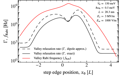
The dependence of on , for a moderate drive amplitude V/m, is shown as the solid red (gray) line in Fig. 5; the peak value above Hz corresponds to sub-nanosecond single-qubit gates.
IV.3 Cavity-mediated gate between two valley qubits
Electrically driven valley resonance is enabled by the transverse coupling between the valley qubit and the electric field, that is, the first term in the square bracket in Eq. (IV.1). The same term allows to realize a logical gate on two valley qubits, if both are interacting with an empty mode of an electromagnetic cavityZheng and Guo (2000); Blais et al. (2004). Together with single-qubit operations, this two-qubit gate forms a universal gate setBarenco et al. (1995); Loss and DiVincenzo (1998). For the time of performing the logical gate, the two valley qubits has to be tuned on resonance with each other, , and slightly detuned from the eigenfrequency of the considered cavity mode . The detuning should exceed the qubit-cavity coupling strength , where is the cavity vacuum electric field component along the axis. Assuming that the two valley qubits are identical and feel the same cavity vacuum electric field, the time required to perform the two-qubit gate is
| (8) |
For a numerical estimate of the gate time, we takeTosi et al. ; Salfi et al. (2015) , , implying a qubit-cavity coupling strength of , that is equivalent to a rate of . Then, by choosing the qubit-cavity detuning as , from Eq. (8) we find .
IV.4 Valley-qubit relaxation via phonon emission
Besides allowing for fast coherent control, the relaxation matrix element , together with , also exposes the valley qubit to relaxation processes induced by electrical potential fluctuations. Here, we focus on the example of spontaneous phonon emission: the excited valley qubit can emit a phonon that carries away the qubit-splitting energy, and thereby the qubit relaxes to its ground state. The relaxation process is characterized by the rate . A practical question concerns the ratio of the achievable coherent Rabi frequency and the qubit relaxation rate: the former should be much greater than the latter to have a functional qubit.
The phonon-emission-mediated relaxation process between two electronic states in a silicon QD is described quantitatively in Ref. Tahan and Joynt, 2014: Eq. (6) therein is a formula for the relaxation rate , which is based on the dipole approximation. In our notation, and in the zero-temperature limit, that formula reads
| (9) |
where
| (10a) | |||||
| (10b) | |||||
Here, the following notation is used for the material parameters of silicon: is the mass density, () is the dilational (uniaxial) deformation potential, and () is the longitudinal (transverse) sound velocity. Note that in this approximation, is proportional to the 5th power of the qubit splitting . Recall that in our case, the -directional relaxation matrix element is zero, see Sec. IV.1.
Using our numerically computed relaxation matrix elements (Fig. 4a), we evaluate from Eq. (9), and show the result as the black dashed line in Fig. 5. The key features are as follows. (i) If the step edge is far from the center of the QD (), then is small, of the order of kHz, and it is independent of . (ii) As the wave function overlaps more with the step (), increases with orders of magnitude, and grows above 100 MHz. This is due to the large relaxation matrix element that peaks around the anticrossing point and arises from the valley-to-charge conversion and DQD-type behavior induced by the step. (iii) Somewhat counterintuitively, develops a small dip around the anticrossing point, where the relaxation matrix element has a peak. An interpretation of this dip is obtained by recalling the fact that is proportional to the 5th power of the energy splitting of the qubitTahan and Joynt (2014), and the latter has a minimum at the anticrossing point (see Fig. 3a).
We also compute the relaxation rate exactly, that is, without making the dipole approximation, see Appendix C for details. The result is shown as the solid black line in Fig. 5. The exact is in general smaller than the dipole-approximated one. This is attributed to the phonon bottleneck effectTahan and Joynt (2014). Note that the best correspondence between the exact and dipole approximated results is achieved in the vicinity of the anticrossing point ; this is expected, as the qubit splitting is minimal here, hence the wavelength of the emitted phonon is maximal, and therefore the ratio of the phonon wavelength and the lateral dot size, characterizing the accuracy of the dipole approximation, is maximal.
Finally, we note that Fig. 5 suggests that it is possible to perform many single-qubit operations within the relaxation time of the valley qubit, if the step and the QD overlaps; in particular, at the anticrossing point, .
IV.5 Valley-qubit dephasing due to charge noise
Besides the relaxation process due to electron-phonon interaction, another mechanism of information loss for the valley qubit is dephasing due to fluctuations of the external electric fields. For brevity, we refer to these fluctuations as charge noise. Charge noise can arise, e.g., as a consequence of fluctuating gate voltages or charge traps in the nanostructure. Here, we discuss the relation between the strength of charge noise and the inhomogeneous dephasing time of the valley qubit.
Aiming at order-of-magnitude estimates, we adopt a simple model of charge noise: we assume that the corresponding electric field is random, but homogeneous and quasistatic. Dephasing arises, because the random electric field induces a shift in the valley-qubit energy splitting. The component of the random electric field does not modify , because the step is assumed to have translational invariance along and the homogeneous does not change the shape of the parabolic confinement along . The effects of the and components are discussed separately below.
The component does induce a finite . In fact, the presence of shifts the -directional lateral confinement potential, which is equivalent to shifting the step edge position, which implies a change in the valley qubit splitting as shown in Fig. 3a. For weak noise, can be expressed from the -directional dephasing matrix element as
| (11) |
Note that the anticrossing point is a dephasing sweet spot with respect to -directional charge noise, since the dephasing matrix element vanishes here. There, the relation between and the random electric field is expressed from a second-order expansion as
| (12) |
where
| (13) |
From the numerical data shown in Fig. 3a, we obtain at the anticrossing point, and, from that, we find . Then, we can identify the inhomogeneous dephasing time with the inverse of the typical noise-induced Larmor-frequency detuning, , where denotes standard deviation of . This dependence is shown as the black solid line in Fig. 6.
The component of the random electric field also induces a finite . For weak noise, is expressed as
| (14) |
and hence the dephasing time associated to these -directional charge noise is estimated as , where
| (15) |
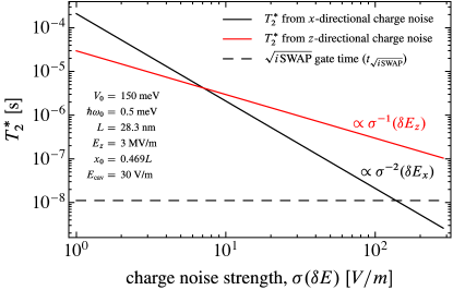
With the concrete parameter values corresponding to the anticrossing point of Fig. 3, we find and . The resulting relation between and is shown as the red (gray) line in Fig. 6.
In Fig. 6, we compare how is influenced by the -directional and -directional components of charge noise. For comparison, we also show, as the dashed horizontal line, the two-qubit gate time ns estimated in section IV.3 (dashed horizontal line). These results suggest that in order to be able to perform at least a few () two-qubit operations within the inhomogeneous dephasing time, the charge noise strength along () should be kept below 40 V/m (200 V/m).
IV.6 Relation to other models and real heterostructures
Our results are based on a modelGamble et al. (2013) where the atomic layers perpendicular to the heterostructure growth direction are represented by continuous planes in which the electrons are described via envelope functions, and a tight-binding descriptionBoykin et al. (2004) accounts for tunnelling between these atomic layers. Within this framework, we provided a clear physical interpretation of our numerical results, in section III. This interpretation is based on the condition that for a step-free silicon/barrier interface, the charge densities of the ground and excited valley-qubit basis states are different on the first atomic layer of silicon. If this condition is satisfied in other, potentially more realistic, models (e.g., accounting for multiple electronic bands, real-space structure of the electronic wave function, disorder effects in the barrier material, etc) and in real heterostructures, then we expect that the conclusions drawn from the model used here remain true at least on a qualitative level.
V Conclusions
We have analysed the influence of a single-atom high barrier step on the dynamics of a single electron confined to a silicon quantum dot. We were focusing on the spectral and dynamical characteristics of the single-electron valley qubit, that is, the two lowest-energy orbital states of the QD. We have found that placing the quantum dot over the step has a strong influence on the properties of the valley qubit. (i) The wave functions of the two valley-qubit basis states are deformed differently, leading to a mechanism of valley-to-charge conversion, potentially useful for non-demolition readout of the valley qubit. (ii) The presence of the step, together with an ac electrical excitation (induced by one of the confinement gates, for example), can be utilized for resonant control of the valley qubit (electrically driven valley resonance). (iii) Due to the step-induced enhancement of the interaction between the valley qubit and the external electric fields, two-qubit interactions can be mediated by an electromagnetic cavity. (iv) We have demonstrated that the valley-qubit relaxation rate can be enhanced by orders of magnitude in the vicinity of the interface step. (v) In conjunction with the valley-to-charge conversion mechanism, we have demonstrated that a dephasing sweet spot against lateral (-directional) electric field noise can be found if the relative location of the quantum dot and the step edge is set appropriately. Furthermore, we provided estimates for the inhomogeneous dephasing time caused by lateral (-directional) and vertical (-directional) electric field fluctuations.
These results provide insight to the fundamental dynamical processes associated to the valley degree of freedom in imperfect silicon quantum dots, and an initial assessment of how the functionality of a valley qubit is influenced by the presence of a barrier step at the silicon/barrier interface. Besides that, we think that the results presented here will also contribute to the understanding of spin-qubit dynamics in silicon quantum dots, which is often strongly influenced by the valley degree of freedom.
Acknowledgements.
We thank S. Coppersmith, M. Eriksson, M. Friesen, A. Dzurak, W. Huang, M. Veldhorst, N. Zimmerman and R. Joynt for useful discussions. We acknowledge funding from the EU Marie Curie Career Integration Grant CIG-293834, OTKA Grants No. PD 100373 and 108676, the Gordon Godfrey Bequest, and the EU ERC Starting Grant 258789. A. P. was supported by the János Bolyai Scholarship of the Hungarian Academy of Sciences.Appendix A Further details of the model
In section II, we specify the model describing the energies and wave functions of the valley-qubit basis states and . Here, we provide a few further details of the model and the numerical procedure.
(1) The triangular quantum well along , hosting the QD, is modelled using a double-barrier structure. The site index runs between -49 and 134, the upper barrier (shown in Fig. 1) is the region , the silicon quantum well is the region , and the lower barrier (not shown in Fig. 1) is the region . Correspondingly, the function , introduced in section II after Eq. (1), representing the spatial range of the barrier material, is specified as
| (16) | |||||
| (17) | |||||
| (18) | |||||
| (19) |
(2) To obtain the energy eigenvalues and wave functions in the presence of the interface step, we use the following procedure. First, we consider the case when the interface step is absent, and we numerically diagonalize the -directional tight-binding Hamiltonian . The obtained eigenvectors (), together with the harmonic-oscillator eigenstates (), provide a product basis , which is the eigenbasis of the complete Hamiltonian . Then, in the presence of the interface step, the complete Hamiltonian is expanded in the truncated product basis, where and , and the resulting matrix is diagonalized numerically. Note that it is sufficient to keep a single -directional harmonic-oscillator eigenstate in the truncated basis, since the interface step has translational invariance along .
Appendix B Interpretation of the wave-function patterns in Fig. 3b
Here, we provide an interpetation of the wave-function patterns (i) and (ii), discussed in section III.
We start from the standard assumption of the envelope-function approximationSaraiva et al. (2011) that and are orthogonal linear combinations of two similar wave packets that are localized in momentum space in the and valleys, respectively:
| (20a) | |||||
| (20b) | |||||
where
| (21) |
Here, is the envelope function, which is spatially slowly varying, ensuring that are indeed localized in the two valleys. The phase can be regarded as a variational parameter, to be determined by the condition that the energy expectation value of should be minimal.
Importantly, the wave functions of Eq. (20) show sinusoidal spatial oscillations with wave number , as seen also in Fig. 3b. Between neighboring lattice sites (distance ), the phase of that oscillation changes by , a value close to . This explains why in Fig. 3b, the quasi-node of at the last barrier layer is followed by a quasi-maximum at the first silicon layer [see (i) in section III]. This pattern of the wave function leads to a minimized potential-energy expectation value: having a wave-function quasi-node at the last barrier layer strongly reduces the potential-energy contribution of barrier, and having a wave-function quasi-maximum at the first silicon layer, which is at the minimum of the -directional confinement potential, is also beneficial.
Finally, the relative phase of between the superpositions in Eq. (20a) and Eq. (20b) implies that the spatial oscillations of are phase-shifted with respect to those of by . Therefore, the wave function of is peaked at the last barrier layer but is close to zero at the first silicon layer [see (ii) in section III].
Appendix C Valley relaxation
Here, we describe how we calculate the valley relaxation rate , discussed in section IV.4, and shown in Fig. 5 as the black solid (exact) and dashed (dipole-approxated) lines.
We start from the zero-temperature Fermi’s Golden Rule:
| (22) |
Here, bras and kets represent joint states of the composite electron-phonon system, denotes the vacuum of phonons, and () is the wave number (polarization index) of the emitted phonon. As for the electron-phonon interaction, we consider the deformation-potential mechanism, and describe it via the Herring-Vogt Hamiltonian:Herring and Vogt (1956); Yu and Cardona (2010)
| (23) |
Here, is the dilational deformation potential, is the uniaxial deformation potential and is the strain tensor. This form of follows from the assumption that the the valley population of the electronic wave function in the QD resides in the and valleys only.
The diagonal elements of the strain tensor, that is, the elements that determine via Eq. (23), read
| (24) |
Here, , is the sample volume and is the polarization vector of the phonon with wave number and polarization index .
Note that from Eq. (24) it follows that transverse phonons do not contribute to the first term of the electron-phonon Hamiltonian in Eq. (23). Furthermore, we define the set of phonons such that their polarization vector lies in the plane. That ensures that the phonons do not contribute to at all.
To obtain the valley relaxation rate , we start from Fermi’s Golden Rule (22), convert the sum for to an integral in spherical coordinates , and perform the radial () integral. This procedure yields
| (25) |
where
| (26a) | ||||
| (26b) | ||||
where
| (30) |
To obtain the exact valley relaxation rate, shown in Fig. 5 as the black solid line, we calculate these integrals numerically, using the rectangle rule and a grid in the integration range . To obtain the dipole-approximated result (9), shown in Fig. 5 as the black dashed line, the dipole approximation is used in Eq. (26), allowing for an analytical evaluation of the angular integrals.
References
- Kane (1998) B. E. Kane, Nature 393, 133 (1998).
- Zwanenburg et al. (2013) F. A. Zwanenburg, A. S. Dzurak, A. Morello, M. Simmons, L. Hollenberg, G. Klimeck, S. Rogge, S. Coppersmith, and M. Eriksson, Rev. Mod. Phys. 85, 961 (2013).
- Feher (1959) G. Feher, Phys. Rev. 114, 1219 (1959).
- Feher and Gere (1959) G. Feher and E. A. Gere, Phys. Rev. 114, 1245 (1959).
- Roth (1960) L. M. Roth, Phys. Rev. 118, 1534 (1960).
- Hasegawa (1960) H. Hasegawa, Phys. Rev. 118, 1523 (1960).
- Simmons et al. (2011) C. B. Simmons, J. R. Prance, B. J. V. Bael, T. S. Koh, Z. Shi, D. E. Savage, M. G. Lagally, R. Joynt, M. Friesen, S. N. Coppersmith, and M. A. Eriksson, Phys. Rev. Lett. 106, 156804 (2011).
- Raith et al. (2011) M. Raith, P. Stano, and J. Fabian, Phys. Rev. B 83, 195318 (2011).
- Tahan and Joynt (2014) C. Tahan and R. Joynt, Phys. Rev. B 89, 075302 (2014).
- Bermeister et al. (2014) A. Bermeister, D. Keith, and D. Culcer, Appl. Phys. Lett. 105, 192102 (2014).
- Kha et al. (2015) A. Kha, R. Joynt, and D. Culcer, Appl. Phys. Lett. 107, 172101 (2015).
- Itoh and Watanabe (ions) K. M. Itoh and H. Watanabe, arXiv:1410.3922 (to be published in MRS Communications).
- Yu and Cardona (2010) P. Y. Yu and M. Cardona, Fundamentals of Semiconductors (Springer, Berlin, 2010).
- Morello et al. (2010) A. Morello, J. J. Pla, F. A. Zwanenburg, K. W. Chan, H. Huebl, M. Mottonen, C. D. Nugroho, C. Yang, J. A. van Donkelaar, A. D. C. Alves, D. N. Jamieson, C. C. Escott, L. C. L. Hollenberg, R. G. Clark, and A. S. Dzurak, Nature 467, 687 (2010).
- Tracy et al. (2010) L. A. Tracy, E. P. Nordberg, R. W. Young, C. B. Pinilla, H. L. Stalford, G. A. T. Eyck, K. Eng, K. D. Childs, J. Stevens, M. P. Lilly, M. A. Eriksson, and M. S. Carroll, Appl. Phys. Lett. 97, 192110 (2010).
- Pla et al. (2012) J. J. Pla, K. Y. Tan, J. P. Dehollain, W. H. Lim, J. J. L. Morton, D. N. Jamieson, A. S. Dzurak, and A. Morello, Nature 489, 541 (2012).
- Pla et al. (2013) J. J. Pla, K. Y. Tan, J. P. Dehollain, W. H. Lim, J. J. L. Morton, F. A. Zwanenburg, D. N. Jamieson, A. S. Dzurak, and A. Morello, Nature 496, 334 (2013).
- Veldhorst et al. (2014) M. Veldhorst, J. C. C. Hwang, C. H. Yang, A. W. Leenstra, B. de Ronde, J. P. Dehollain, J. T. Muhonen, F. E. Hudson, K. M. Itoh, A. Morello, and A. S. Dzurak, Nat Nano 9, 981 (2014).
- Muhonen et al. (2014) J. Muhonen, J. Dehollain, A. Laucht, F. Hudson, T. Sekiguchi, K. Itoh, D. Jamieson, J. McCallum, A. Dzurak, and A. Morello, Nature Nanotechnology 9, 986 (2014).
- Kawakami et al. (2014) E. Kawakami, P. Scarlino, D. R. Ward, F. R. Braakman, D. E. Savage, M. G. Lagally, M. Friesen, S. N. Coppersmith, M. A. Eriksson, and L. M. K. Vandersypen, Nature Nanotech. 9, 666 (2014).
- Veldhorst et al. (2015a) M. Veldhorst, C. H. Yang, J. C. C. Hwang, W. Huang, J. P. Dehollain, J. T. Muhonen, S. Simmons, A. Laucht, F. E. Hudson, K. M. Itoh, A. Morello, and A. S. Dzurak, Nature 526, 410 (2015a).
- Weber et al. (2014) B. Weber, Y. H. M. Tan, S. Mahapatra, T. F. Watson, H. Ryu, R. Rahman, L. C. L. Hollenberg, G. Klimeck, and M. Y. Simmons, Nat. Nano. 9, 430 (2014).
- Cullis and Marko (1970) P. R. Cullis and J. R. Marko, Phys. Rev. B 1, 632 (1970).
- Koiller et al. (2001) B. Koiller, X. Hu, and S. Das Sarma, Phys. Rev. Lett. 88, 027903 (2001).
- Boykin et al. (2004) T. B. Boykin, G. Klimeck, M. Friesen, S. N. Coppersmith, P. von Allmen, F. Oyafuso, and S. Lee, Phys. Rev. B 70, 165325 (2004).
- Wellard and Hollenberg (2005) C. J. Wellard and L. C. L. Hollenberg, Phys. Rev. B 72, 085202 (2005).
- Friesen et al. (2007) M. Friesen, S. Chutia, C. Tahan, and S. N. Coppersmith, Phys. Rev. B 75, 115318 (2007).
- Culcer et al. (2010) D. Culcer, L. Cywiński, Q. Li, X. Hu, and S. Das Sarma, Phys. Rev. B 82, 155312 (2010).
- Friesen and Coppersmith (2010) M. Friesen and S. N. Coppersmith, Phys. Rev. B 81, 115324 (2010).
- Salfi et al. (2014) J. Salfi, J. A. Mol, R. Rahman, G. Klimeck, M. Y. Simmons, L. C. L. Hollenberg, and S. Rogge, Nat. Mater. 13, 605 (2014).
- Nestoklon et al. (2006) M. O. Nestoklon, L. E. Golub, and E. L. Ivchenko, Phys. Rev. B 73, 235334 (2006).
- Li and Dery (2011) P. Li and H. Dery, Phys. Rev. Lett. 107, 107203 (2011).
- Huang and Hu (2014) P. Huang and X. Hu, Phys. Rev. B 90, 235315 (2014).
- Veldhorst et al. (2015b) M. Veldhorst, R. Ruskov, C. Yang, J. Hwang, F. Hudson, M. Flatté, C. Tahan, K. Itoh, A. Morello, and A. Dzurak, Phys. Rev. B 92, 201401 (2015b).
- Saraiva et al. (2011) A. L. Saraiva, M. J. C. R. B. Capaz, X. Hu, S. Das Sarma, and B. Koiller, Phys. Rev. B 84, 155320 (2011).
- Lim et al. (2011) W. H. Lim, C. H. Yang, F. A. Zwanenburg, and A. S. Dzurak, Nanotechnology 22, 335704 (2011).
- Wu and Culcer (2012) Y. Wu and D. Culcer, Phys. Rev. B 86, 035321 (2012).
- Culcer et al. (2012) D. Culcer, A. Saraiva, X. Hu, B. Koiller, and S. Das Sarma, Phys. Rev. Lett. 108, 126804 (2012).
- Yang et al. (2013) C. H. Yang, A. Rossi, R. Ruskov, N. S. Lai, F. A. Mohiyaddin, S. Lee, C. Tahan, G. Klimeck, A. Morello, and A. S. Dzurak, Nat. Comm. 4, 2069 (2013).
- Kim et al. (2014) D. Kim, Z. Shi, C. B. Simmons, D. R. Ward, J. R. Prance, T. S. Koh, J. K. Gamble, D. E. Savage, M. G. Lagally, M. Friesen, S. N. Coppersmith, and M. A. Eriksson, Nature 511, 70 (2014).
- Hao et al. (2014) X. Hao, R. Ruskov, M. Xiao, C. Tahan, and H. Jiang, Nature Comm. 5, 3860 (2014).
- Recher et al. (2007) P. Recher, B. Trauzettel, A. Rycerz, Y. M. Blanter, C. W. J. Beenakker, and A. F. Morpurgo, Phys. Rev. B 76, 235404 (2007).
- Pályi and Burkard (2011) A. Pályi and G. Burkard, Phys. Rev. Lett. 106, 086801 (2011).
- Laird et al. (2013) E. A. Laird, F. Pei, and L. P. Kouwenhoven, Nat. Nanotech. 8, 565 (2013).
- Széchenyi and Pályi (2014) G. Széchenyi and A. Pályi, Phys. Rev. B 89, 115409 (2014).
- Laird et al. (2015) E. A. Laird, F. Kuemmeth, G. A. Steele, K. Grove-Rasmussen, J. Nygård, K. Flensberg, and L. P. Kouwenhoven, Rev. Mod. Phys. 87, 703 (2015).
- Kormányos et al. (2014) A. Kormányos, V. Zólyomi, N. D. Drummond, and G. Burkard, Phys. Rev. X 4, 011034 (2014).
- Wu et al. (2016) Y. Wu, Q. Tong, G.-B. Liu, H. Yu, and W. Yao, Phys. Rev. B 93, 045313 (2016).
- Gamble et al. (2013) J. K. Gamble, M. A. Eriksson, S. N. Coppersmith, and M. Friesen, Phys. Rev. B 88, 035310 (2013).
- Nowack et al. (2007) K. C. Nowack, F. H. L. Koppens, Y. V. Nazarov, and L. M. K. Vandersypen, Science 318, 1430 (2007).
- Golovach et al. (2006) V. N. Golovach, M. Borhani, and D. Loss, Phys. Rev. B 74, 165319 (2006).
- Zheng and Guo (2000) S.-B. Zheng and G.-C. Guo, Phys. Rev. Lett. 85, 2392 (2000).
- Blais et al. (2004) A. Blais, R.-S. Huang, A. Wallraff, S. M. Girvin, and R. J. Schoelkopf, Phys. Rev. A 69, 062320 (2004).
- Barenco et al. (1995) A. Barenco, C. H. Bennett, R. Cleve, D. P. DiVincenzo, N. Margolus, P. Shor, T. Sleator, J. A. Smolin, and H. Weinfurter, Phys. Rev. A 52, 3457 (1995).
- Loss and DiVincenzo (1998) D. Loss and D. P. DiVincenzo, Phys. Rev. A 57, 120 (1998).
- (56) G. Tosi, F. A. Mohiyaddin, S. B. Tenberg, R. Rahman, G. Klimeck, and A. Morello, ArXiv:1509.08538v1.
- Salfi et al. (2015) J. Salfi, J. A. Mol, D. Culcer, and S. Rogge, arXiv:1508.04259 (2015).
- Herring and Vogt (1956) C. Herring and E. Vogt, Phys. Rev. 101, 944 (1956).