Tellurene-a monolayer of tellurium from first-principles prediction
Abstract
A two dimensional (2D) Group-VI Te monolayer, tellurene, is predicted by using first-principles calculations, which consists of four-membered planner and six-membered chair-like rings arranged alternately in a 2D lattice. The phonon spectra calculations, combined with ab initio molecular dynamics (MD) simulations, demonstrate that tellurene is kinetically stable. The tellurene shows a desirable direct band gap of 1.04 eV and its band structure can be effectively tuned by strain. The effective mass calculations imply that tellurene should also exhibit a relatively high carrier mobility, e.g. compared with MoS2. The significant direct band gap and the high carrier mobility imply that tellurene is a very promising candidate for a new generation of nanoelectronic devices.
keywords:
Tellurene, first-principles study, ab initio molecular dynamics, band structure, effective massContributed equally to this work \altaffiliationContributed equally to this work \alsoaffiliationCenter for Advanced Analysis and Computional Science, Zhengzhou University, Zhengzhou 450001, China \alsoaffiliationKey Laboratory for Special Functional Materials(MOE), Henan University, Kaifeng, China
1 Introduction
Research in 2D materials, as inspired by the development of graphene, has experienced an explosive increase in recent years due to their rather unique and exceptional properties with promising applications in electronic, photonic, energy and environmental devices. The 2D group-IV materials including silicene,1 germanene 2 and stanene 3 have been realized experimentally after graphene. For group-V elements, few-layer black phosphorus, named phosphorene, 4, 5, 6 has also been successfully fabricated by exfoliation, which exhibits prominent properties such as high carrier mobility and high on/off ratio. Very recently, the novel 2D group-III material of borophene has been fabricated successfully.7, 8 Beside the allotropes of single element in 2D family, the 2D transition metal dichalcogenides, such as MoS2, 9 MoSe2, WS2 10, 11 and WSe2 12, 13, have been synthesized and attracted both experimental and theoretical interests because of their relatively large and direct band gap as well as good carrier mobilities. To the best of our knowledge, except these binary compounds containing chalcogen, 2D monolayered structures of simple group VI elements has not been reported before.
The group-VI elements possess a valence configuration of , and their stable structures show systematic change from diatomic molecules (O) through rings, chains and helices (S, Se, Te) to the only simple cubic lattice found in one element (Po). The most stable structure of Te at the atmospheric pressure is a trigonal one, which consists of helical chains parallel to the c-axis,14 and each atom covalently bonds to two neighbors within a chain while the interchain bonding is relatively weak. This inherent anisotropy makes it an ideal candidate for the generation of 1D nanostructures. For example, 1D Te nanocrystals, including Te nanotubes, nanorods, nanowires, and nanobelts, have been synthesized through different routes.15, 16, 17, 18, 19, 20
Despite the strong tendency to grow into one-dimensional nanoarchitecture, it is also possible for Te to form 2D structure. Recently, the hexagonal Te nanoplates have been successfully realized on flexible mica sheets via van der Waals epitaxy.21 However, the Te hexagonal nanoplate has a thickness about 32 nm, which is different from the atomically thinned 2D crystal. Although one monolayer of Te has been tried to deposite on the CdTe (111) surface with the molecular beam epitaxy method,22 the crystal structure of 2D monolayer Te could not be determined because of the strong covalent bonding between the adsorbed Te atoms and substrate. Therefore, whether the 2D monolayer structure can be realized in the scope of chalcogen, just as succeeded in carbon group and pnictogens, is still an open question.
Here, we investigated the possibilities of 2D materials for chalcogen based on first-principles calculations, and a novel 2D semiconductor, namely tellurene (Te monolayer), is predicted. It is composed of planner four-membered and chair-like six-membered rings alternately arranged in a 2D lattice. The monolayer tellurene shows a direct band gap of 1.04 eV. Interestingly, both the band gap and transport properties of tellurene can be tuned by strains, which make it promising in applications such as electronic and optoelectronic devices.
2 Results and discussion
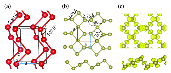
As the reference, the optimized structure of trigonal tellurium (t-Te) is a monoclinic phase with space group P3121, which consists of helical chains arranged in a hexagonal array along c direction, shown in Figure 1a. Figure 1b presents the proposed structure of tellurene, which is composed of planner four-membered and chair-like six-membered rings arranged alternately in a 2D lattice. The optimized unit cell is spanned by lattice vectors and , with a = 5.49 Å and b = 4.17 Å, respectively. In tellurene, Te atom favors threefold and fourfold coordinations instead of the twofold coordination in its bulk counterpart. The short and long bonds are 2.75 and 3.01 Å, respectively. The van der Waals radii of the Te atom is about 2.36 Å 23 which indicates that covalent bonds are dominant in tellurene. As shown in Figure 1c, the calculated charge density difference illustrates that, besides the strong covalent bonds between two Te atoms with the coordination number (CN) of three, the Te atoms with CN = 4 also bond to its four neighbor Te atoms. The vanished strong interlayer van der Waals interactions in t-Te may play an important role in the structure transition from bulk helical chains to the hypervalent monolayer structure. The atoms of tellurene are much closer together than those of bulk phase, due to the vanished van der Waals interactions.
To examine the relative stability of tellurene, the formation energy is studied by calculation of the cohesive energy difference = (3D)- (2D), where (2D) and (3D) are the cohesive energies in the 2D tellurene and 3D structure of t-Te, respectively. In general, this is the energy cost to synthesize the single-layer material from its three-dimensional bulk counterpart. The lower formation energy indicates that the candidate single-layer material is more stable. The calculated of tellunene is 0.23 eV/atom, much smaller than the formation energies of silicene (0.76 eV/atom) and germanene (0.99 eV/atom) having been experimentally fabricated, 24, 1, 2 which indicates that tellurene is also expected to be synthesized in the experiment.
Actually, it is very important to examine the stability and feasibility in experiment for new 2D crystals. Phonon calculations, reflecting whether there are soft modes, provide a criterion to judge the structure stability.25 Hence, the phonon spectrum is examined, shown in Figure 2 (left panel). It is clearly revealed no soft phonon modes in the computed phonon dispersion spectrum of tellurene, predicting that tellurene is kinetically stable. The displacement patterns corresponding to the six optical modes at point are plotted in right panels in Figure 2, which illustrate the different characteristics of bond stretching and bending . Among these displacement patterns, (a) and (d) correspond to the LO modes at point, (c) and (e) correspond to the TO modes, and (b) and (f) correspond to the two ZO modes, respectively. Mode (a) results in a diametric expansion/contraction in the basal plane, and the harder Mode (f) corresponds to rotational motion.
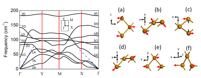
To further understand the stability and structural rigidity of tellurene, the slopes of the longitudinal acoustic branches near point, which correspond to the speed of sound and reveal the in-plane stiffness, are calculated. As seen in Figure 2, the speed of sound in tellurene is along the -Y direction, and along the -X direction. The speed of sound along the -Y direction is faster than that along -X, which reflects an anisotropy in the elastic constants of tellurene. The lower rigidity along the -X direction, corresponding to the direction in Figure 1b, reflects the fact that compression along the armchair direction requires primarily bond bending, which is lower in energy cost than bond stretching. The anisotropic characters of the elastic constants in tellurene are similar to that in phosphonene.26 Furthermore, the calculated flexural rigidity D also provides a quantitative explanation for the anisotropy in the elastic constants of tellurene, which can be extracted from total energy of nanotube with different diameter. The calculation details are presented in the Support Information (Figure S1). We have estimated along the armchair direction and along the zigzag direction for tellurene, respectively.
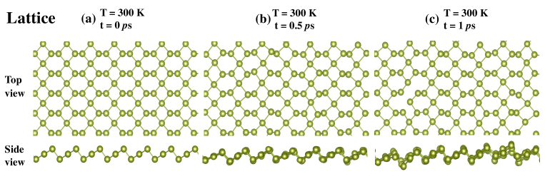
To further clarify the stability of tellurene at elevated temperatures, we performe the ab initio MD calculations of the monolayer as well as flakes. The temperatures are kept at 300 and 1000 K, respectively, covering time periods up to 1 ps with a time step of 1 fs. The high rigidity of a free-standing tellurene monolayer is confirmed by the MD calculations at nonzero temperatures. As shown in Figure 3, the infinite monolayer of tellurene exhibits slight changes at room temperature, revealing the high structural rigidity. The detailed results are presented in the Supplemental Information (Figure S2 and movies).
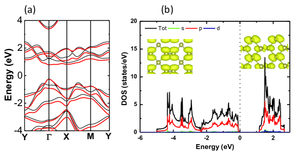
The band structures and the electron density of states are also calculated to explore the electronic properties of tellurene, shown in Figure 4. It is distinctly found that the spin-orbital coupling (SOC) has a significant influence on the electronic structure of tellurene. As shown in Figure 4a, the band structure shows an indirect band gap without SOC, but exhibits a direct band gap of 1.04 eV with SOC. Figure 4b presents the calculated total and partial DOS of tellurene. It is obviously manifested that the DOS near the Fermi level is predominantly p like states with almost negligible contributions of s and d electrons. To gain further insights into the electronic structure, the spatial distributions of the valence band maximum (VBM) and the conduction band minimum (CBM) of tellurene are also examined (Insets of Figure 4b). Both the VBM and CBM originate mainly from the p atomic orbitals, and the VBM is bonding-like along the armchair direction while CBM is antibonding-like state.
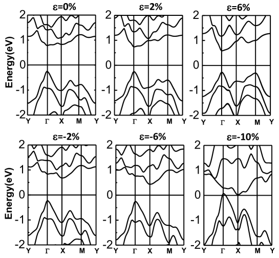
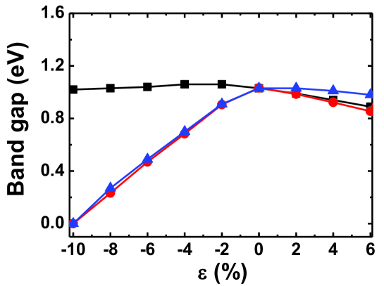
It has been shown that applying external strain is an effective way to tune the electronic properties of 2D materials.27, 28, 29 The band gap of tellurene also depends sensitively on the applied in-layer strain. Figure 5 presents the band structures of tellurene under the biaxial strains from -10% to 6%. It is found that CBM shifts down gradually towards the Fermi Level as the tensile strain increases from 0% to 6%, whereas the energy of VBM almost does not change, resulting in the reduced band gap, and the band gap reduced to 0.86 eV under the tensile strain of 6%. This manifests that the band gap of stretched tellurene is dominated by the CBM. Nevertheless, the stretched tellurene still retains the character of direct band gap. On the other hand, the monolayer tellurene undergoes a direct-to-indirect band-gap transition under the compressed strain. It is found that a relatively small critical strain about -2% can induce a direct-to-indirect band gap transition. The CBM shifts from to X point under the compressed strain, which rapidly transforms tellurene into an indirect band gap semiconductor. In tellurene, the bonds among Te atoms may have the dual characteristics of metal and covalence, and there exists a competition between them in the strained stages. The covalent bonding may be dominant under the stretched strain, which will decrease the bonding between the p orbitals, leading to the separation of bonding and antibonding states getting smaller near the Fermi level. On the other hand, the metal bonding characteristic may be critical when the tellurene is compressed. The overlaps between p orbitals of Te atoms will be strengthened as the compressed strain increases, which improves the power of charge transportation. Meanwhile, the band gap becomes small and presents a metallic character under = -10%.
In order to better understand the strain effects on the electronic properties of tellurene, uniaxial strains along armchair and zigzag directions of the lattice are also applied, respectively (Figure S3 and Figure S4). The results suggest that the strain effects of tellurene exhibit very strong anisotropy. As shown in Figure 6, the compressed strain along the zigzag direction critically influences the electronic structure, which modulates the band gap of tellurene, similar to that of biaxial strain. However, the band gap does not change much along armchair direction under the compressed strain from 0% to -10%. Moreover, the tensile strain along the armchair direction shows more significant effect on tuning the band structure of tellurene than that along the zigzag direction from = 0% to 6%.
One of the main interests in 2D semiconductors is the observed high mobility of carriers such as graphene and phosphorene. In order to provide further insights into the charge transport properties of tellurene, the effective masses of electrons at the CBM (m) and of holes at the VBM (m) are calculated using
where E and k correspond to the energy and the reciprocal lattice vector along the axis. In solid theory, it is thought that the charge carrier mobility is inversely proportional to the effective mass if there is no change in the time scale for quasi particle scattering. Based on this, we can simply define the mobility as
According to the above formula, changes in effective mass can influence charge carrier transport properties. Under zero strain, the effective electron masses are m= 0.83 m0 and m=0.19 m0, and the effective hole masses are m= 0.39 m0 and m=0.12 m0, respectively. Here, m0 is the mass of electron. The effective mass of hole is lower than that of the electron which indicates that the carrier mobility is dominated by holes in intrinsic monolayer tellurene. Compare with the effective electron mass m= 0.48 m0 of monolayer MoS2 30, it is likely that tellurene will exhibit a higher carrier mobility than monolayer MoS2.
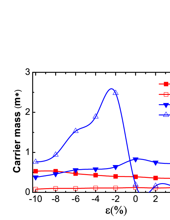
The variations of effective masses of hole and electron with the biaxial strain are also studied in tellurene, presented in Figure 7. The results suggest that the compressed strain significantly affects the electron effective mass, i.e. strongly influences the electron transport of tellurene. The m shows a significant jump at the maximum values of 2.48 m0 under the compressed strain of -2%, and subsequently decreases with the strain from -2% to -10%. This result can be also reflected in the band structure variations with strain, in which the CBM shifts from to X resulting in the transition from direct to indirect band gap semiconductor. On the other hand, the m decreases from 0.83 m0 under = 0% to 0.36 m0 under = -10%. However, the tensile strain does not modify the effective masses much between = 0% and 6%.
The electronic and hole effective masses under the uniaxial strains are also examined (Figure S5 and Figure S6). Although it slightly modifies the band gap of tellurene, the compressed strain along the armchair direction critically influences the electronic effective masses. The m decreases from 3.20 m0 under = -2% to 1.73 m0 under = -10%. In addition, the m can also be effectively tuned from 0.42 m0 to 0.75 m0 between = -2% and -10%. On the other hand, it is found that the compressed strain from = -4% to -10% along the zigzag direction does not cause much change in the m. The tensile strain leads to an increase of m from 0.63 m0 under = 0% to 1.07 m0 under = 6%. Surprisingly, the m undergoes a significant jump from 0.51 m0 under = -8% to 1.51 m0 under = -10%.
From the above analysis of the behavior of the effective mass, it is likely that the proposed tellurene may exhibit a higher carrier mobility than MoS2. Moreover, the transport properties can be modified by both biaxial and uniaxial strains. The combination of a significant band gap and a high carrier mobility implies that tellurene is a highly promising candidate for a new generation of nanoelectronic devices.
In summary, a 2D group-VI material, tellurene, has been predicted for the first time. It is composed of planner four-membered and chair-like six-membered rings arranged alternately in a 2D lattice. The monolayer tellurene shows a direct band gap of 1.04 eV. In addition, both the band gap and transport properties of tellurene can be tuned by external strain. All these characteristics make tellurene a highly promising candidate for applications in electronic, photonic and optoelectronic devices.
3 Methods
All calculations are performed within the density functional theory (DFT) using the Vienna ab initio Simulation Package (VASP).31 The projected augmented wave (PAW) potentials 32, 33 are adopted to treat the core electrons, and the Perdew-Burke-Ernzerhof (PBE) exchange-correlation functional 34 is employed. The unit cell including a vacuum of 15 Å is used to simulate the 2D monlayer crystal. For Brillouin zone (BZ) integration, the Monkhorst-Pack scheme 35 with a 15 15 1 k-point grid is used. The kinetic energy cutoff for the plane wave basis set is chosen to be 500 eV. All structures are fully relaxed until the total energies are converged up to eV and the Hellmann-Feynman forces are less than 0.02 eV/Å. The phonon calculations employ a supercell approach, as implemented in the Phonopy code.36 In the ab initio MD simulations, the temperatures are kept at 300 and 1000 K for 1 ps with a time step of 1 fs. The van der Waals effect is treated using the DFT-D2 method of Grimme.37
Flexural rigidity (D) calculations of tellurene, ab initio MD simulations of infinite monolayer as well as a free-standing finite flake of tellurene at high temperatures, uniaxial strain effects on the band structures, effective masses modulated by uniaxial strains.
The authors gratefully acknowledge financial support from the National Natural Science Foundation of China (No. 11274280 and 11504332 ), the National Basic Research Program of China (No. 2012CB921300), the Natural Science Foundation of Henan Province of China (No.152300410049) and the Key Scientific Research Project of Henan Province (No. 16A140019). The calculations are performed on the High Performance Clusters of Zhengzhou University. ZXG also acknowledge the support of the UK EPSRC (No. EP/K021192/1).
References
- Feng et al. 2012 Feng, B.; Ding, Z.; Meng, S.; Yao, Y.; He, X.; Cheng, P.; Chen, L.; Wu, K. Nano letters 2012, 12, 3507–3511
- Dávila et al. 2014 Dávila, M.; Xian, L.; Cahangirov, S.; Rubio, A.; Le Lay, G. New Journal of Physics 2014, 16, 095002
- Zhu et al. 2015 Zhu, F.-f.; Chen, W.-j.; Xu, Y.; Gao, C.-l.; Guan, D.-d.; Liu, C.-h.; Qian, D.; Zhang, S.-C.; Jia, J.-f. Nature materials 2015, 14, 1020–1025
- Li et al. 2014 Li, L.; Yu, Y.; Ye, G. J.; Ge, Q.; Ou, X.; Wu, H.; Feng, D.; Chen, X. H.; Zhang, Y. Nature nanotechnology 2014, 9, 372–377
- Xia et al. 2014 Xia, F.; Wang, H.; Jia, Y. Nature communications 2014, 5
- Zhu et al. 2014 Zhu, Z.; Li, C.; Yu, W.; Chang, D.; Sun, Q.; Jia, Y. Applied Physics Letters 2014, 105, 113105
- Mannix et al. 2015 others,, et al. Science 2015, 350, 1513–1516
- Feng et al. 2015 Feng, B.; Zhang, J.; Zhong, Q.; Li, W.; Li, S.; Li, H.; Cheng, P.; Meng, S.; Chen, L.; Wu, K. arXiv preprint arXiv:1512.05029 2015,
- Lee et al. 2010 Lee, C.; Yan, H.; Brus, L. E.; Heinz, T. F.; Hone, J.; Ryu, S. ACS nano 2010, 4, 2695–2700
- Elias et al. 2013 Elias, A. L.; Perea-López, N.; Castro-Beltrán, A.; Berkdemir, A.; Lv, R.; Feng, S.; Long, A. D.; Hayashi, T.; Kim, Y. A.; Endo, M. Acs Nano 2013, 7, 5235–5242
- Gutiérrez et al. 2012 Gutiérrez, H. R.; Perea-López, N.; Elías, A. L.; Berkdemir, A.; Wang, B.; Lv, R.; López-Urías, F.; Crespi, V. H.; Terrones, H.; Terrones, M. Nano letters 2012, 13, 3447–3454
- Huang et al. 2013 Huang, J.-K.; Pu, J.; Hsu, C.-L.; Chiu, M.-H.; Juang, Z.-Y.; Chang, Y.-H.; Chang, W.-H.; Iwasa, Y.; Takenobu, T.; Li, L.-J. ACS nano 2013, 8, 923–930
- Liu et al. 2013 Liu, W.; Kang, J.; Sarkar, D.; Khatami, Y.; Jena, D.; Banerjee, K. Nano letters 2013, 13, 1983–1990
- Donohue 1974 Donohue, J. The structure of the Elements, 1st ed.; John Wiley and Sons: New York, 1974
- Mo et al. 2002 Mo, M.; Zeng, J.; Liu, X.; Yu, W.; Zhang, S.; Qian, Y. Advanced Materials 2002, 14, 1658–1662
- Zhou and Zhu 2006 Zhou, B.; Zhu, J.-J. Nanotechnology 2006, 17, 1763
- Lu et al. 2004 Lu, Q.; Gao, F.; Komarneni, S. Advanced Materials 2004, 16, 1629–1632
- Li et al. 2004 Li, X.-L.; Cao, G.-H.; Feng, C.-M.; Li, Y.-D. Journal of Materials Chemistry 2004, 14, 244–247
- Zhang et al. 2007 Zhang, B.; Hou, W.; Ye, X.; Fu, S.; Xie, Y. Advanced Functional Materials 2007, 17, 486–492
- Song et al. 2008 Song, J.-M.; Lin, Y.-Z.; Zhan, Y.-J.; Tian, Y.-C.; Liu, G.; Yu, S.-H. Crystal Growth and Design 2008, 8, 1902–1908
- Wang et al. 2014 Wang, Q.; Safdar, M.; Xu, K.; Mirza, M.; Wang, Z.; He, J. ACS nano 2014, 8, 7497–7505
- Ren et al. 2016 others,, et al. ACS applied materials & interfaces 2016,
- Batsanov 2001 Batsanov, S. Inorganic materials 2001, 37, 871–885
- Cahangirov et al. 2009 Cahangirov, S.; Topsakal, M.; Aktürk, E.; Şahin, H.; Ciraci, S. Physical review letters 2009, 102, 236804
- Li et al. 2014 Li, Y.; Liao, Y.; Chen, Z. Angewandte Chemie International Edition 2014, 53, 7248–7252
- Zhu and Tománek 2014 Zhu, Z.; Tománek, D. Physical review letters 2014, 112, 176802
- Morgan Stewart et al. 2015 Morgan Stewart, H.; Shevlin, S. A.; Catlow, C. R. A.; Guo, Z. X. Nano letters 2015, 15, 2006–2010
- Zhang et al. 2015 Zhang, S.; Li, C.; Guo, Z. X.; Cho, J.-H.; Su, W.-S.; Jia, Y. Nanotechnology 2015, 26, 295402
- Han et al. 2014 Han, X.; Morgan Stewart, H.; Shevlin, S. A.; Catlow, C. R. A.; Guo, Z. X. Nano letters 2014, 14, 4607–4614
- Kaasbjerg et al. 2012 Kaasbjerg, K.; Thygesen, K. S.; Jacobsen, K. W. Physical Review B 2012, 85, 115317
- Kresse and Furthmüller 1996 Kresse, G.; Furthmüller, J. Physical Review B 1996, 54, 11169
- Blöchl 1994 Blöchl, P. E. Physical Review B 1994, 50, 17953
- Kresse and Joubert 1999 Kresse, G.; Joubert, D. Physical Review B 1999, 59, 1758
- Perdew et al. 1996 Perdew, J. P.; Burke, K.; Ernzerhof, M. Physical review letters 1996, 77, 3865
- Monkhorst and Pack 1976 Monkhorst, H. J.; Pack, J. D. Physical Review B 1976, 13, 5188
- Togo et al. 2008 Togo, A.; Oba, F.; Tanaka, I. Physical Review B 2008, 78, 134106
- Zacharia et al. 2004 Zacharia, R.; Ulbricht, H.; Hertel, T. Physical Review B 2004, 69, 155406