First-principles study of the optoelectronic properties and photovoltaic absorber layer efficiency of Cu-based chalcogenides
Abstract
Cu-based chalcogenides are promising materials for thin-film solar cells with more than 20% measured cell efficiency. Using first-principles calculations based on density functional theory, the optoelectronic properties of a group of Cu-based chalcogenides Cu2-II-IV-VI4 is studied. They are then screened with the aim of identifying potential absorber materials for photovoltaic applications. The spectroscopic limited maximum efficiency (SLME) introduced by Yu and Zunger is used as a metric for the screening. After constructing the current-−voltage curve, the maximum spectroscopy–dependent power conversion efficiency is calculated from the maximum power output. The role of the nature of the band gap, direct or indirect, and also of the absorptivity of the studied materials on the maximum theoretical power conversion efficiency is studied. Our results show that Cu2II-GeSe4 with II=Cd and Hg, and Cu2-II-SnS4 with II=Cd and Zn have a higher theoretical efficiency compared to the materials currently used as absorber layer.
pacs:
71.15.Mb, 88.40.fc, 88.40.jn
I Introduction
The potential applications of the multinary chalcogenide semiconductors in optoelectronics give rise to an intense interest in their design and synthesis that dates back to the 1950s Katagiri et al. (2008); Schorr et al. (2007); Parasyuk et al. (2005); Matsushita et al. (2000). Ternary I-III-VI2 compounds can be generated from binary II-VI chalcogenides through substituting group II atoms by pairs of group I and III atoms. Because of the increased chemical and structural flexibility in ternary compounds, they exhibit a larger variety of optoelectronic properties compared to binary ones Chen et al. (2009). For example, CuGaSe2 has a band gap of 1.68 eV which is lower than that of ZnSe (2.82 eV) Madelung (2004). This is one of the characteristics of CuGaSe2 that makes it convenient for application in thin-film solar cells. Further flexibility is obtained by introducing quaternary chalcogenides and this allows to engineer the functional properties to satisfy a certain application, e.g. high-efficiency photovoltaic absorber layers or light emitting diodes.
There are two approaches to substitute the cations in ternary I-III-VI2 to design quaternary compounds.
One is to replace two III atoms by one II and one IV atom, forming a I2-II-IV-VI4 compound.
The other one is to replace one I atom and one III atom by two II atoms, forming
II2-I-III-VI4 compounds. Such quaternary chalcogenides with I = Cu, Ag, II = Zn, Cd,
III = Ga, In, IV = Ge, Sn, and VI = S, Se, Te
have been synthesized by different groups Schorr et al. (2007); Parasyuk et al. (2001, 2005).
In particular, Cu-based chalcogenides Cu2-II-IV-VI4 can be found at
the center of various technological innovations.
Among these compounds, Cu2ZnSnS4 (CZTS) and Cu2ZnSnSe4 (CZTSe)
combine promising characteristics for optoelectronic applications
(e.g. direct band gap of 1.0-1.4 eV, a high optical absorption coefficient up to ,
and a relatively high abundance of the elements Todorov et al. (2013); Barkhouse et al. (2012); Matsushita et al. (2000)).
Such characteristics make them the low-cost alternative to the conventional
photovoltaic materials like Si, CdTe and CuIn1-xGaxSe2 Todorov et al. (2013); Barkhouse et al. (2012).
While significant attention has been paid to CZTS and CZTSe Katagiri et al. (2008); Scragg et al. (2008); Altosaar et al. (2008),
most of the other compounds in this family remain relatively unexplored.
Limited theoretical attention has been paid to these chalcogenides,
so their electronic structure and optical properties remain unclear,
which limits their usage in semiconductor devices.
A deeper knowledge of their optoelectronic properties
might bring further improvements in their applications Siebentritt (2013).
On the one hand, extensive measurements have been performed to study the change of the power
conversion efficiency of the photovoltaic solar cells with respect to the characteristics of
the absorber layers. On the other hand, the conversion efficiency of the solar cells is
investigated theoretically, but very few of such studies calculate the efficiency of the
solar cells using first-principles methods.
Some successful first-principles studies have identified new materials with high conversion efficiency
for PV applications Yu and Zunger (2012); Yin et al. (2014); Lee et al. (2014).
Yu and Zunger introduced the ”spectroscopic limited maximum efficiency (SLME)”
which is a theoretical power efficiency that can be investigated using first-principles
calculated quantities. They used the SLME parameter as a selection metric to
identify new absorber materials Yu and Zunger (2012).
One of the features of the SLME is including the effect of the thickness in the efficiency of the absorber layer which is not taken into account in the well known maximum theoretical efficiency, Shockley–-Queisser (SQ) limit Shockley and Queisser (1961). The thickness of the absorber layers in the existing thin film solar cells is few
micrometers Jger et al. (2015). If this thickness could be reduced with only minor loss in
performance of the solar cell, the production costs could be lowered.
Calculating the SLME of a material provides insight about how thin that material can be made with no
significant loss in its efficiency.
One of the main goals of the present manuscript is to investigate how the optoelectronic properties of
the Cu2-II-IV-VI4 compounds change by modifying the material composition.
Moreover, we propose some potential new absorber materials using the SLME parameter.
II Structure of the chalcogenides materials
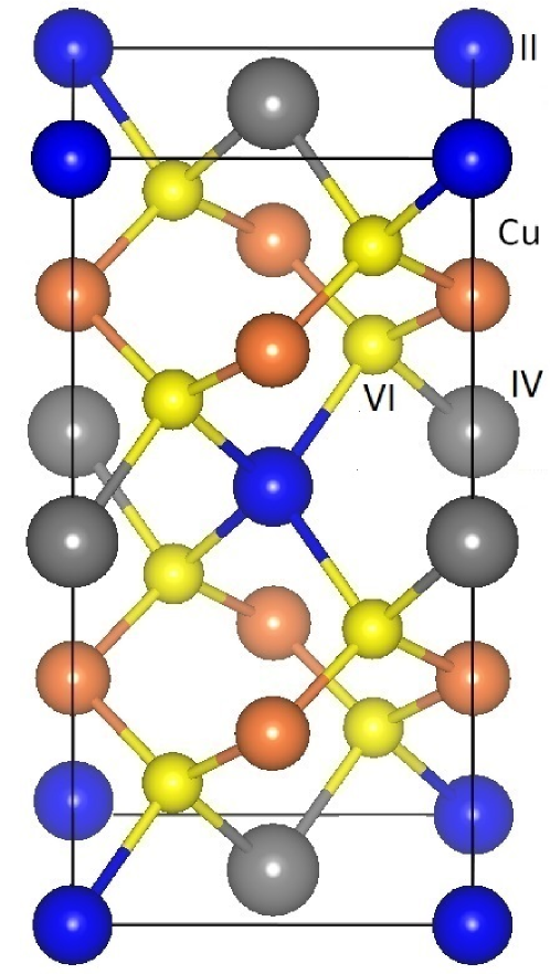
The distribution of the cations within the unit cell of Cu2-II-IV-VI4 depends on the nature of the group II and IV atoms. For example the kesterite structure is the most stable phase for Cu2ZnSnSe4 Schorr (2011), while it is reported that Cu2CdSnSe4 and Cu2HgSnSe4 prefer the stannite structure as the energetically favorable one Olekseyuk et al. (2002); Liu et al. (2009a). Because of the limited number of studies on the stannite structure of the quaternary Cu-based chalcogenides, the optoelectronic properties of the compounds are not not well-known. We investigate a group of Cu-based materials that can be found in the stannite structure: Cu2-II-IV-VI4 with II = Cd, Hg, and Zn, IV = Sn, and Ge, and VI = S, Se, and Te.
Stannite Cu2-II-IV-VI4 compounds are quaternary complexes with a crystal structure similar to the zinc-blende structure of ZnS and the kesterite structure of CuInS2. The stannite primitive cell (space group Ia2m, No. 121) contains 8 atoms.
Figure 1 presents the stannite structure. There are alternating cation layers of mixed II and IV atoms, which are separated from each other by layers of Cu monovalent cations. Each anions is tetrahedrally coordinated by four cations. Two equivalent Cu atoms occupy the 4d Wyckoff position (site symmetry S4), one II atom on 2a, one IV atom on 2b (both II and IV with D2d symmetry) and four VI atoms on 8i position (site symmetry Cs). In this structure, each anion has thereby three inequivalent bonds(VI-Met) with the cations Met = Cu, Zn, and Sn.
III Computational Method
Our ab initio computations are based on DFT Hohenberg and Kohn (1964); Kohn and Sham (1965), and are carried out using the VASP code Kresse and Hafner (1993, 1994); Kresse and Furthmüller (1996a, b). We use PAW Kresse and Joubert (1999); Blöchl (1994) potentials to describe the electron-ion interaction. We use the generalized gradient approximation (GGA) to the exchange-correlation potential, in the PBE parametrization Perdew et al. (1996) to perform all structural calculations. Electronic structure and optical properties are calculated using the HSE06 hybrid functional Wang and Pickett (1983). An energy cutoff of 350 eV is used for the plane-wave basis set. For structural relaxation and total energy calculations the Brillouin Zone was sampled using a 444 Monkhorst-Pack (MP) grid Monkhorst and Pack (1976). Atomic relaxations were made until residual forces on the atoms were less than 0.01 eV/Å and total energies were converged to within 1 meV.
In order to calculate the absorption spectra, the imaginary part of the dielectric function () tensor is obtained using the random phase approximation, as implemented in the VASP code Gajdos et al. (2006). The dielectric function tensor of the studied compounds that have the tetragonal structure can be described completely by two non-zero independent components, namely , and which corresponds to the dielectric function along the x-, and z-direction, respectively. The real part of the dielectric function is obtained from the imaginary part through the Kramers-Kronig relation. We found that it is enough to sample the Brillouin zone using a 101010 MP grid to obtain a converged tensor. The number of unoccupied bands used here is 3 times the number of occupied bands.
Since the photovoltaic conversion efficiency strongly depends on the band gap, it is important to get an accurate value from our first-principles calculations. It is known that standard DFT calculations, using local or semi-local exchange-correlation functionals such as the local density approximation (LDA) or GGA, seriously underestimate the band gap of semiconductors Johnson and Ashcroft (1998); Wang and Pickett (1983), while the hybrid functional HSE06 has proven to be capable of giving close-to-experiment predictions for a large range of compounds including Cu-based compounds Henderson et al. (2011); Yu and Zunger (2012). Moreover, for a series of compounds, HSE06 provides a dielectric function in much better agreement with experiment than GGA or LDA functionals Tang et al. (2012); Wan et al. (2013).
We calculate the power conversion efficiency of an absorber layer which is defined as , where is the maximum output power density and is the total incident solar power density. can be obtained by numerically maximizing the where is current density and stands for voltage. The total current density for a solar cell illuminated under the photon flux at temperature is given by Green (2003). In this work, the standard AM1.5G solar spectrum at 25 is used AM1 (2013). Consistently, all parameters that contribute to the SLME and SQ limit are calculated for .
The first term in the formula is the short-circuit current density given by
| (1) |
where is the elementary charge and is the photon absorptivity. The second term is the reverse saturation current density or loss current density is calculated using the formula
| (2) |
where is the Boltzmann constant, and is the temperature. , corresponding to the total electron-hole recombination current density at equilibrium in the dark. This recombination includes both nonradiative and radiative current densities, where is the fraction of the radiative recombination current. is approximated by where Yu and Zunger (2012). In equilibrium the rates of emission and absorption through cell surfaces should be equal in the dark. Thus, the rate of black-body photon absorption from the surrounding thermal bath through the front surface of the cell gives
| (3) |
where is the black-body spectrum Tiedje et al. (1984). With modeled as , can be calculated. is the absorption spectrum of the material and is the thin film thickness.
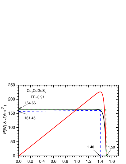
We also address some characteristics of the solar cell such as the fill factor (FF). FF represents the fraction of the maximum power that can be obtained from the cell and it is the ratio between and . is simply the product of the highest value of the voltage and current density of the solar cell, . The open circuit voltage () which is the voltage of the solar cell under is calculated using the formula
| (4) |
IV Results
IV.1 Electronic structure and optical properties
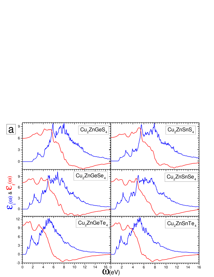
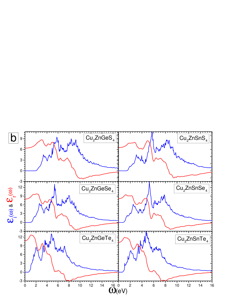
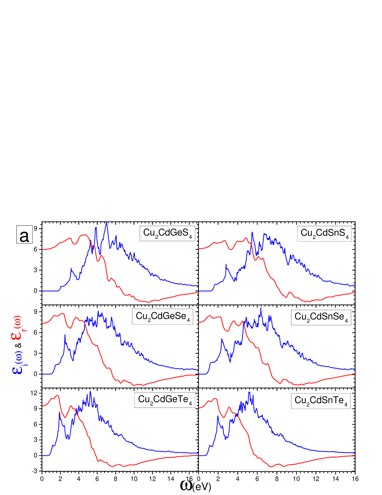
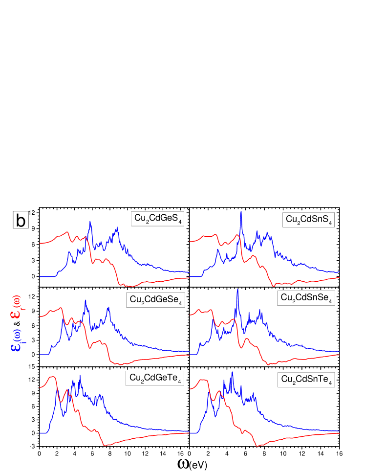
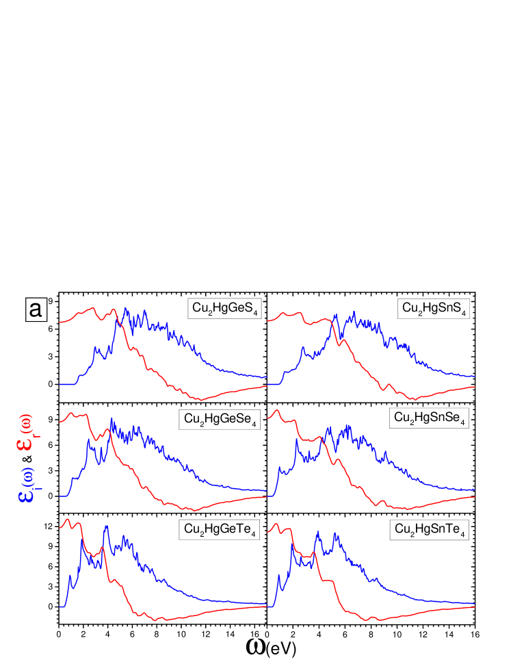
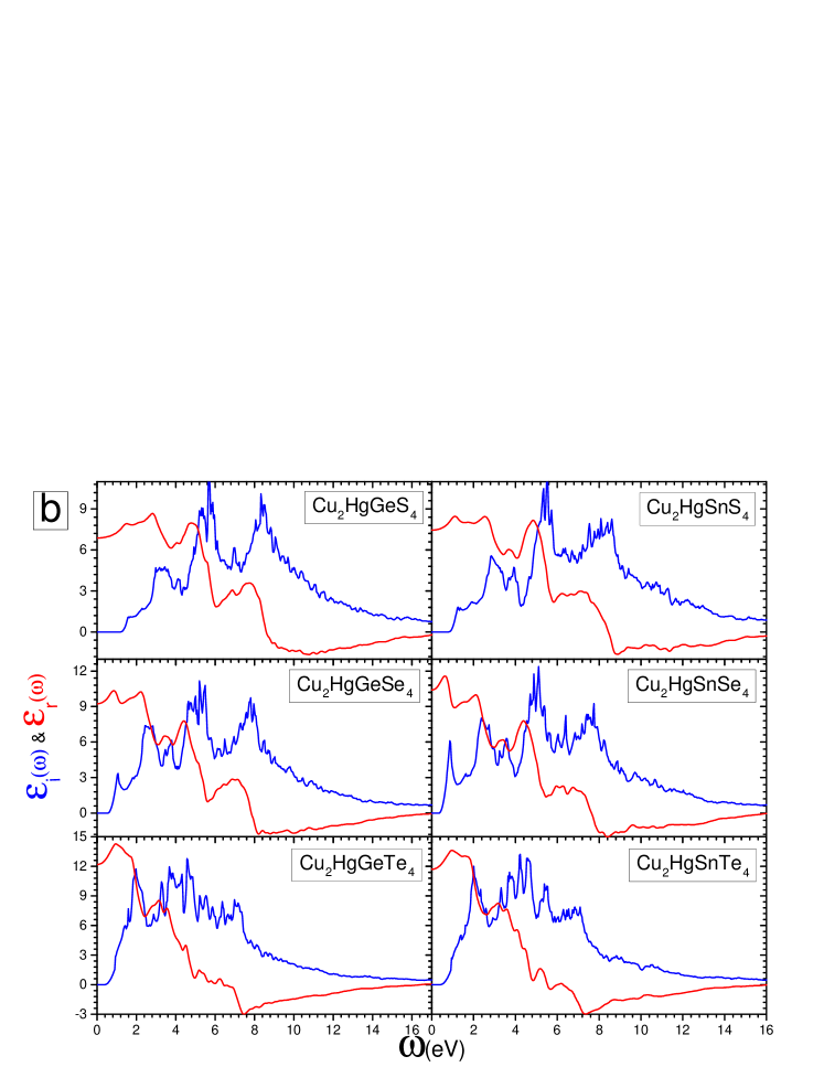
In order to calculate the current density, the absorptivity of the compound should be calculated (cf. Eqs. 1 and 3). Using the dielectric function, the absorption spectra and absorptivity are calculated. Figures A.1- A.3 in Appendix A show the imaginary () and real () parts of the dielectric function for Cu-based chalcogenides along the x-, and z-direction, , and , respectively. We have noticed that the intensity of the peaks in and the value of the optical dielectric constant () along the z-direction are larger than those corresponding to the x-direction. This results in a higher value of the refractive index along the z-direction compared with the one along the x-direction. It means that the birefringent studied compounds are optically uniaxial and they all have positive birefringence.


Two aspects of the low frequency behavior of the dielectric function are relevant to experiment. One is the absorption edge, determined by onset of the imaginary part of the dielectric function. The other one is zero frequency limit of the real part of the dielectric function, i.e. the optical dielectric constant which is given in table LABEL:table-S1. Table LABEL:table-S1 shows that in each family of chalcogenides, e.g. Cu2HgGe-VI4, by replacing the element VI by one from the same group and with higher atomic number, there is an increase in . Such an increase in indicates that the polarizability of the system tends to increase because of increasing ionicity of the bonds. Replacing S with Se and then by Te (i.e. increasing the ionic radius) results in a more extended electron cloud that screens the electric field more effectively and yields higher polarizability. One can see that the plasma frequency () decreases with the same substitution. Given that the number of valence electrons is the same for all of the studied chalcogenides, the decrease of can be understood as a consequence of the increased lattice constant on replacing an atom by a larger one.
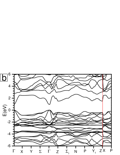
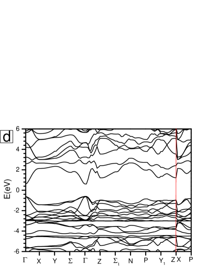
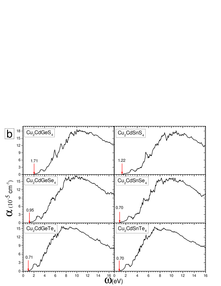
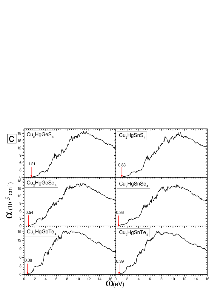
The energy of the first direct allowed transition (optical band gap) can be found from the absorption spectra. Figs. A.4(a)-(c) present the arithmetic average of the absorption spectra. By replacing element VI by an element with a higher atomic number there is a red shift in the absorption edge and the band gap also shows the same trend. Moreover, from comparing the electronic band structure with the absorption spectrum we see that the first transition is direct and allowed. The electronic band structure of four typical chalcogenides is shown in Figs. 2(a)-(d).
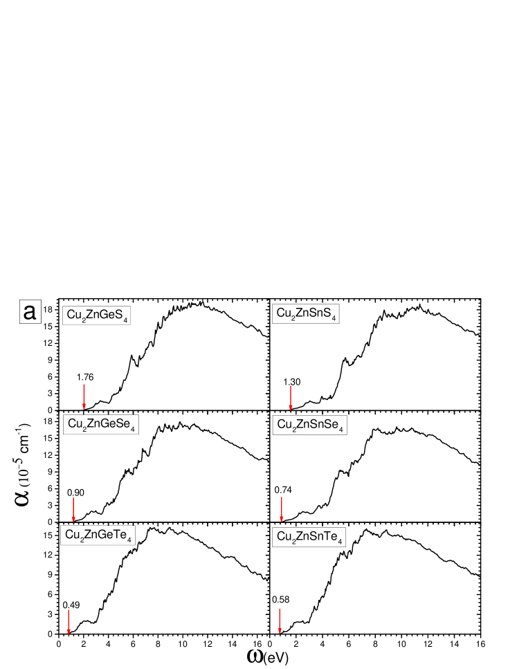
It is important for an absorber layer to highly absorb most part of the solar spectrum and specifically the visible light. Substituting S by Se and then by Te (the VI element) increases the maximum absorption of the Cu2-II-IV-VI4 compounds in the visible range (1.65 to 3.23 eV). For example, the maximum absorption of Cu2HgGeS4, Cu2HgGeSe4, and Cu2HgGeTe4 is 2.21, 2.40, and 4.17 cm-1, respectively. The opposite trend is found for the optical band gap. It means that the optical band gap of Cu2HgGeS4, 1.21 eV is larger than that of Cu2HgGeSe4, 0.54 eV, and Cu2HgGeTe4, 0.38 eV.
IV.2 Power conversion efficiency
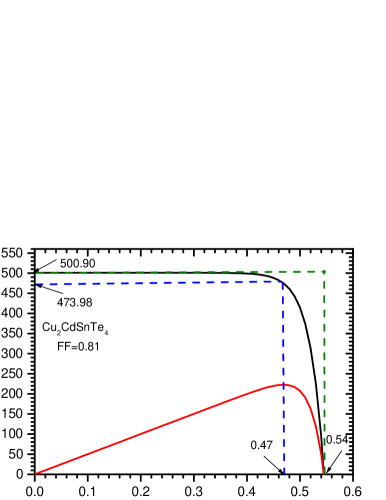
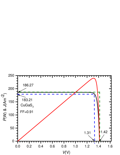
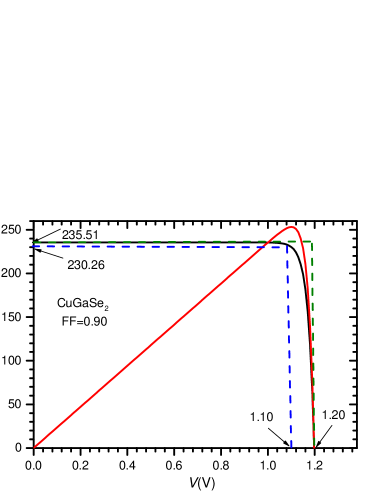
In order to calculate the SLME from the maximum output power of the absorber layer, we first plot
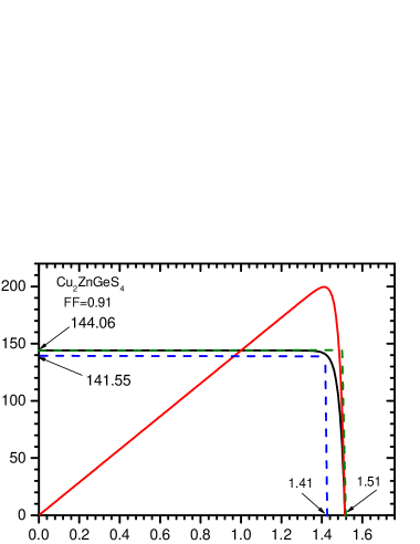
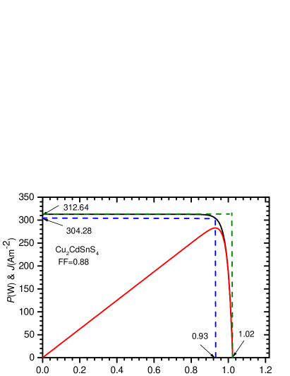
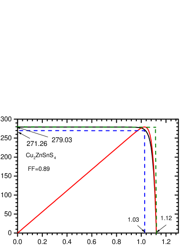
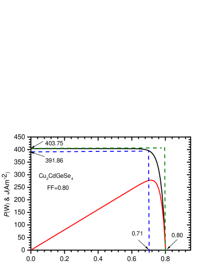
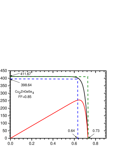
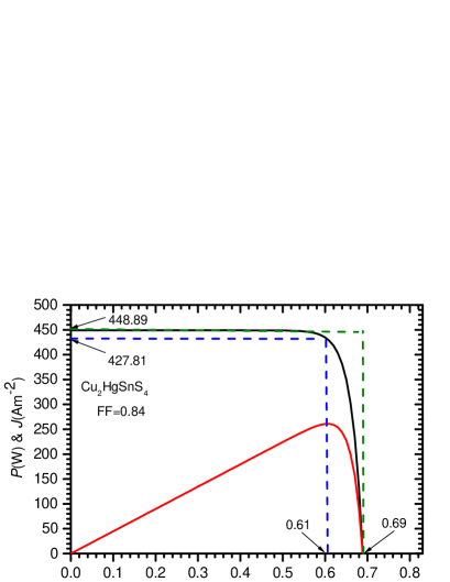
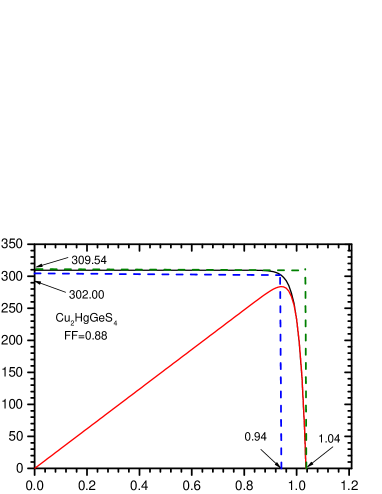
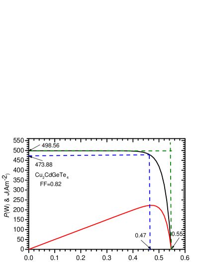
the current-voltage (J-V) and power-voltage (P-V) curve for the chalcogenides with an SLME below the corresponding SQ limit (See Fig. 3).
As indicated later the SLME criterion can lead to anomalous results where the SLME value is beyond the SQ limit. We therefore limit ourselves to those compounds with an SLME value below the SQ limit.
The same plot is shown for two common thin-film solar cell materials, CuGaS2, and CuGaSe2.
The voltage is the difference between the quasi Fermi level for electrons and holes.
This value can be changed by applying an electric field (i.e. via incident photons on
the solar cell). The voltage changes between zero and its maximum value which is of the material.
and are presented by blue and green dashed lines, respectively.
Figure 3 also gives , and .
For each compound, the lower voltage is , and the higher one corresponds to
. Each plot gives two more values, namely (lower one) and (higher one).
According to the definition of and , is always larger than and
this difference depends on the recombination rate.
Likewise, Eq. 4 implies that is always larger than .
Altogether, is always larger by a factor (FF) than . The FF values are given
for each compound in the corresponding plot in Fig 3.
The - plot shows a large of 411.67 Am-2 for Cu2ZnGeSe4.
However, this compound has a small compared with the others that results in low output power,
FF, and efficiency. On the other hand, Cu2CdGeS4 with low has a
large that yields a large efficiency and largest FF.
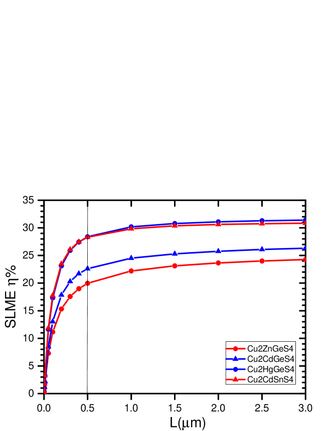
Typical absorber layers (e.g. Cu{In,Ga}Se2) are a few micrometers thick, further decrease in thickness is desirable to reduce processing times and material usage Jger et al. (2015). However, there is a limit on the thickness of the absorber layer based on the desirable efficiency value. The SLME depends on the film thickness and it increases as increases. It converges to the corresponding SQ limit for very large thicknesses of the considered film. In fact, the materials with the same band gap might have different rate of the convergence because of their different optical properties. Finding a material that converges fast to the SQ limit is desirable. Figure 4 represents the SLME as a function of thin film thickness for four studied chalcogenides. On the one hand, there is a slight increase in the efficiency by increasing the film thickness for values larger than 0.5 m. On the other hand, by making the film thinner than 0.5 m the SLME diminishes. This means that we cannot make the absorber layer thinner than 0.5 m without loosing too much of its efficiency. Therefore, we use m for the thickness of the studied absorber layers.
Figure 4 shows two materials, Cu2CdSnS4 and Cu2HgGeS4 with almost the same band gap resulting in very similar efficiencies within the SQ limit. In the range of sub-micrometer thicknesses, the difference in the SLME values mainly results from the different corresponding optical properties.
Figure 5 presents the SLME parameter for the studied compounds as a function of the band gap energy. The calculated SLME value for two well-known absorber layer materials (CuGaS2, and CuGaSe2) is also represented. The SQ limit as the upper limit on the efficiency is also given as a curve.
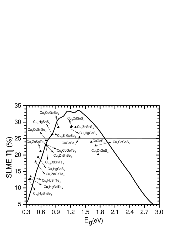
One can see from Fig. 5 that the SLME value of some of the considered compounds is higher than the corresponding SQ limit, which is a theoretical upper limit for the efficiency of the absorber layer. In a separate publication we analyze this anomaly in more detail Bercx et al. . Nevertheless, as shown by Yu and Zunger Yu and Zunger (2012) the SLME is more powerful than the SQ limit in ranking the compounds based on their power conversion efficiency by including the optical properties of the materials. For example a comparison between Cu2CdGeSe4 and Cu2ZnSnS4 shows that it is possible to have a high efficiency absorber layer with a non-optimum band gap material. Cu2CdGeSe4 has a band gap of 0.95 eV and the band gap of Cu2ZnSnS4 is 1.30 eV. According to the SQ limit, the latter is expected to have a higher efficiency. However, the former compound has a higher absorption that results in a higher efficiency.
Nevertheless, SLME is more powerful than SQ limit in ranking the compounds based on their power conversion efficiency by including the optical properties of the materials. This fact can be understood by making a comparison between the studied compounds. For example a comparison between Cu2CdGeSe4 and Cu2ZnSnS4 shows that it is possible to have a high efficiency absorber layer with a non-optimum band gap material. Cu2CdGeSe4 has a band gap of 0.95 eV and the band gap of
Cu2ZnSnS4 is 1.30 eV. According to the SQ limit, the latter is expected to
have a higher efficiency. However, the former compound has a higher absorption that results in
a higher efficiency.
Based on Fig. 5 our calculations identify four quaternary Cu-based chalcogenides, namely Cu2CdGeSe4, Cu2CdSnS4, Cu2HgGeS4, and Cu2ZnSnS4, as possible absorber layers with a power efficiency higher than 25%.
Their theoretical efficiency stays considerably above the other studied chalcogenides. The latter identified material is already used as an absorber layer in photovoltaic cells.
Its SLME value differs by 8% from that of Ref. Yin et al. (2014), where the absorption spectrum was calculated using the GGA functional. It is already proven that
HSE06 provides a dielectric function in much better agreement with experiment than GGA or
LDA functionals Tang et al. (2012); Wan et al. (2013).
The measured cell efficiency for CZTS is 12.6% lower than its SLME value Wang et al. (2013) because of (i) the difference between solar cell and absorber layer and (ii) the presence of electron–hole recombination centers. The latter should be prohibited to get the maximum theoretical power conversion efficiency.
Further studies on the formation of native defects in the identified compounds are required to
understand better the power conversion efficiency limit applied to these materials.
We also calculate the band structure and optical properties for CuGaS2, and CuGaSe2.
The HSE06 calculations result in 1.62, and 1.38 eV band gap for CuGaS2, and CuGaSe2, respectively.
There is an 33%, and 17% underestimation with respect to the experiment band gap for CuGaS2, and CuGaSe2, respectively Madelung (2004).
We calculate 24%, and 25.33% for the SLME of the considered compounds. A comparison between our results with existing results that used the GW approximation for the band gap calculation Yu and Zunger (2012) and HSE for the optical properties shows 7.5% and 1.3% difference in the SLME value for these compounds.
However, both calculations result in a higher band gap and a higher SLME for CuGaSe2.
V Conclusion
The results of the present work show that the optoelectronic properties of the studied Cu-based chalcogenides Cu2-II-IV-VI4 strongly depend on the element VI in the composition of the material. The change of element VI has a higher effect than changing element II, or IV in altering the characteristics of the studied chalcogenides. Replacement of the element VI by one from the same group with a higher atomic number decreases the plasma frequency and band gap and at the same time results in an increase of the lattice parameters, and optical dielectric constant. A clear red shift in the absorption edge is observed which is correlated with the decrease in the band gap. Further studies of the compounds of interest show that besides the fundamental band gap that plays a main role in the efficiency of an absorber layer, the absorption coefficient is an essential characteristic. The absorption coefficient is important to compare the efficiency of two compounds with the same band gap. In that case two compounds have the same SQ efficiency, but the one with higher absorptivity has a higher SLME value. Finally, the results of the calculations identify Cu2II-GeSe4 with II=Cd, and Hg and Cu2-II-SnS4 with II=Cd, and Zn as high efficiency absorber layers.
VI Acknowledgements
We acknowledge the financial support from the FWO-Vlaanderen through project G.0150.13N and a GOA fund from the University of Antwerp. The computational resources and services used in this work were provided by the VSC (Flemish Supercomputer Center) and the HPC infrastructure of the University of Antwerp (CalcUA), both funded by the FWO-Vlaanderen and the Flemish Government–department EWI.
Appendix A
Table LABEL:table-S1 presents the list of studied stannite Cu-based chalcogenides in the following order: Cu2Zn-based, Cu2Cd-based, and then Cu2Hg-based compounds. For each compound, the first row presents the calculated HSE06 results, and the following rows contain the available experimental and theoretical data.
| Compound | a | c/a | Eg | Hf | (, ) | |
|---|---|---|---|---|---|---|
| Cu2ZnGeS4 | 5.30 | 2.02 | 1.76 | -2.99 | 19.62 | 6.09 (5.96, 6.37) |
| 5.34iiiParasyuk et al. (2005) | 1.97iiiParasyuk et al. (2005) | 2.04iiiChen and Ravindra (2013) | ||||
| 5.33ivChen and Ravindra (2013) | 2.06ivChen and Ravindra (2013) | 2.14viChen and Ravindra (2013) | 6.8ivChen and Ravindra (2013) | |||
| Cu2ZnGeSe4 | 5.60 | 2.01 | 0.90 | -2.31 | 18.16 | 7.56 (7.36, 7.97) |
| 5.63iiiBhaskar et al. (2013) | 1.96iiiBhaskar et al. (2013) | 1.29iiiChen and Ravindra (2013) | ||||
| 5.38ivChen and Ravindra (2013) | 2.02ivChen and Ravindra (2013) | 1.32viChen and Ravindra (2013) | 9.01ivChen and Ravindra (2013) | |||
| Cu2ZnGeTe4 | 6.04 | 1.99 | 0.49 | -3.21 | 16.53 | 10.17 (9.89, 10.73) |
| 5.60iiiParasyuk et al. (2005) | 1.99iiiParasyuk et al. (2005) | |||||
| 6.09ivChen and Ravindra (2013) | 2.00ivChen and Ravindra (2013) | 0.55viChen and Ravindra (2013) | 17.93ivChen and Ravindra (2013) | |||
| Cu2ZnSnS4 | 5.42 | 2.01 | 1.30 | -3.15 | 19.00 | 6.25 (6.12, 6.53) |
| 5.44iiiPaier et al. (2009) | 2.01iiiPaier et al. (2009) | 1.29iiiPaier et al. (2009) | 6.48iiiPaier et al. (2009) | |||
| 5.34vZhao and Persson (2011) | 2.01vZhao and Persson (2011) | 1.27vZhao and Persson (2011) | 6.99v(z)Zhao and Persson (2011) | |||
| Cu2ZnSnSe4 | 5.71 | 2.00 | 0.71 | -4.23 | 16.37 | 7.74 (7.56, 8.12) |
| 5.61iiiShen et al. (2012) | 1.99iiiShen et al. (2012) | 1.41iiiLiu et al. (2009b) | ||||
| 5.61vZhao and Persson (2011) | 1.99vZhao and Persson (2011) | 0.69vZhao and Persson (2011) | 8.19(x), 8.27(z)vZhao and Persson (2011) | |||
| Cu2ZnSnTe4 | 6.13 | 2.00 | 0.58 | -2.24 | 16.38 | 9.74 (9.53, 10.17) |
| 6.20iiiShen et al. (2012) | 1.99iiiShen et al. (2012) | 0.5iiiShen et al. (2012) | 14iiiShen et al. (2012) | |||
| 6.20ivShen et al. (2012) | 1.99ivShen et al. (2012) | |||||
| Cu2CdGeS4 | 5.52 | 1.91 | 1.71 | -3.97 | 19.02 | 6.06 (6.24, 7.88) |
| 5.34iiiJambor and Roberts (1999) | 1.97iiiJambor and Roberts (1999) | |||||
| Cu2CdGeSe4 | 5.79 | 1.92 | 0.95 | -3.08 | 18.46 | 7.51 (7.33, 7.88) |
| 5.75iiiPiskach et al. (2000) | 1.92iiiPiskach et al. (2000) | 1.20iiiPiskach et al. (2000) | ||||
| Cu2CdGeTe4 | 6.20 | 1.93 | 0.71 | -2.24 | 16.36 | 9.78 (9.50, 10.33) |
| 6.13iiiOlekseyuk et al. (2002) | 1.94iiiOlekseyuk et al. (2002) | |||||
| Cu2CdSnS4 | 5.62 | 1.940 | 1.22 | -3.74 | 18.68 | 6.25 (6.10, 6.56) |
| 5.59iiiSchafer and Nitsche (1977) | 1.94iiiSchafer and Nitsche (1977) | 1.45iiiGuan et al. (2013) | ||||
| Cu2CdSnSe4 | 5.88 | 1.95 | 0.70 | -4.01 | 17.74 | 7.72 (7.47, 8.23) |
| 5.81iiiHahn and Schulze (1965) | 1.97iiiHahn and Schulze (1965) | 0.96iiiIbánez et al. (2012) | ||||
| Cu2CdSnTe4 | 6.27 | 1.97 | 0.70 | -2.28 | 16.19 | 9.44 (9.16, 9.99) |
| 6.20iiiHaeuseler et al. (1991) | 1.98iiiHaeuseler et al. (1991) | |||||
| Cu2HgGeS4 | 5.52 | 1.92 | 1.21 | -3.05 | 19.43 | 6.79 (6.75, 6.87) |
| 5.49iiiSchäfer and Nitsche (1974) | 1.92iiiSchäfer and Nitsche (1974) | |||||
| Cu2HgGeSe4 | 5.79 | 1.92 | 0.54 | -3.14 | 18.40 | 8.90 (8.74, 9.23) |
| 5.69iiiHahn and Schulze (1965) | 1.93iiiHahn and Schulze (1965) | |||||
| Cu2HgGeTe4 | 6.19 | 1.94 | 0.38 | -1.74 | 17.06 | 11.93 (11.81, 12.18) |
| 6.11iiiOlekseyuk et al. (2002) | 1.95iiiOlekseyuk et al. (2002) | |||||
| Cu2HgSnS4 | 5.61 | 1.95 | 0.83 | -2.78 | 19.10 | 7.08 (6.90, 7.45) |
| 5.57iiiKabalov et al. (1998) | 1.95iiiKabalov et al. (1998) | |||||
| Cu2HgSnSe4 | 5.88 | 1.95 | 0.36 | -2.28 | 18.12 | 9.58 (9.17, 10.40) |
| 5.83iiiOlekseyuk et al. (2002) | 1.96iiiOlekseyuk et al. (2002) | 0.17iiiMkrtchyan et al. (1988) | ||||
| 5.84ivLi et al. (2012) | 1.97ivLi et al. (2012) | 13.78ivLi et al. (2012) | ||||
| Cu2HgSnTe4 | 6.20 | 1.97 | 0.39 | -1.71 | 16.15 | 11.38 (11.21, 11.70) |
| 6.19iiiOlekseyuk et al. (2002) | 1.98iiiOlekseyuk et al. (2002) | |||||
| i The GGA functional is used for the calculation of the formation energy. | ||||||
| ii and represent the value of an arithmetic average with respect to the direction of polarization. | ||||||
| iii Experimental results. | ||||||
| iv Theoretical results using GGA functional. | ||||||
| v Theoretical results using HSE06 functional. | ||||||
| vi Theoretical results using GGA functional. A rigid shift is applied to correct the band gapChen and Ravindra (2013) . | ||||||
| , and is the optical dielectric constant along x-, and z- direction respectively. | ||||||
| (x), and (z) refer to in the x-, and z-direction, respectively. | ||||||
References
- Katagiri et al. (2008) H. Katagiri, K. Jimbo, S. Yamada, T. Kamimura, W. S. Maw, T. Fukano, T. Ito, and T. Motohiro, Appl. Phys. Express 1, 041201 (2008).
- Schorr et al. (2007) S. Schorr, G. Wagner, M. Tovar, and D. Sheptyakov, Mater. Res. Soc. Symp. Proc. 1012, Y03 (2007).
- Parasyuk et al. (2005) O. V. Parasyuk, I. D. Olekseyuk, and L. V. Piskach, J. Alloy. Compd. 397, 169 (2005).
- Matsushita et al. (2000) H. Matsushita, T. Maeda, A. Katsui, and T. Takizawa, J. Cryst. Growth 208, 416 (2000).
- Chen et al. (2009) S. Chen, X. G. Gong, A. Walsh, and S. H. Wei, Appl. Phys. Lett. 94, 041903 (2009).
- Madelung (2004) O. M. Madelung, Semiconductors Data Handbook, 3rd ed. (Springer, New York, 2004).
- Parasyuk et al. (2001) O. V. Parasyuk, L. D. Gulay, Y. E. Romanyuk, and L. V. Piskach, J. Alloys Compd. 329, 202 (2001).
- Todorov et al. (2013) T. K. Todorov, J. Tang, S. Bag, O. Gunawan, T. Gokmen, Y. Zhu, and D. B. Mitzi, Adv. Energy Mater. 3, 34 (2013).
- Barkhouse et al. (2012) D. Barkhouse, O. Gunawan, T. Gokmen, T. Todorov, and D. Mitzi, Prog. Photovolt. Res. Appl. 20, 6 (2012).
- Scragg et al. (2008) J. J. Scragg, P. J. Dale, and L. M. Peter, Electrochem. Commun. 10, 639 (2008).
- Altosaar et al. (2008) M. Altosaar, J. Raudoja, K. Timmo, M. Danilson, M. Grossberg, J. Krustok, and E. Mellikov, Phys. Status Solidi A 205, 167 (2008).
- Siebentritt (2013) S. Siebentritt, Thin Solid Films 535, 1 (2013).
- Yu and Zunger (2012) L. Yu and A. Zunger, Phys. Rev. Lett. 108, 068701 (2012).
- Yin et al. (2014) W. J. Yin, T. Shi, and Y. Yan, Adv. Mater. 26, 4653 (2014).
- Lee et al. (2014) I. H. Lee, J. Lee, Y. J. Oh, S. Kim, and K. J. Chang, Phys. Rev. B 90, 115209 (2014).
- Shockley and Queisser (1961) W. Shockley and H. J. Queisser, J. Appl. Phys. 32, 510 (1961).
- Jger et al. (2015) T. Jger, Y. E. Romanyuk, B. Bissig, F. Pianezzi, S. Nishiwaki, P. Reinhard, J. Steinhauser, J. Schwenk, and A. N. Tiwari, J. App. Phys. 117, 225303 (2015).
- Schorr (2011) S. Schorr, Sol. Energy Mater. Sol. Cells 95, 1482 (2011).
- Olekseyuk et al. (2002) I. D. Olekseyuk, L. D. Gulay, I. V. Dydchak, L. V. Piskach, O. V. Parasyuk, and O. V. Marchuk, J. Allo. Comp. 340, 141 (2002).
- Liu et al. (2009a) M. L. Liu, I. W. Chen, F. Q. Huang, and L. D. Chen, Adv. Mater. 21, 3808 (2009a).
- Hohenberg and Kohn (1964) P. Hohenberg and W. Kohn, Phys. Rev. 136, B864 (1964).
- Kohn and Sham (1965) W. Kohn and L. J. Sham, Phys. Rev. 140, A1133 (1965).
- Kresse and Hafner (1993) G. Kresse and J. Hafner, Phys. Rev. B 47, R558 (1993).
- Kresse and Hafner (1994) G. Kresse and J. Hafner, J. Phys. Cond. Matt. 6, 8245 (1994).
- Kresse and Furthmüller (1996a) G. Kresse and J. Furthmüller, Comput. Mater. Sci. 6, 15 (1996a).
- Kresse and Furthmüller (1996b) G. Kresse and J. Furthmüller, Phys. Rev. B 54, 11169 (1996b).
- Kresse and Joubert (1999) G. Kresse and D. Joubert, Phys. Rev. B 59, 1758 (1999).
- Blöchl (1994) P. E. Blöchl, Phys. Rev. B 50, 17953 (1994).
- Perdew et al. (1996) J. P. Perdew, K. Burke, and M. Ernzerhof, Phys. Rev. Lett. 77, 3865 (1996).
- Wang and Pickett (1983) C. S. Wang and W. E. Pickett, Phys. Rev. Lett. 51, 597 (1983).
- Monkhorst and Pack (1976) H. J. Monkhorst and J. D. Pack, Phys. Rev. B 13, 5188 (1976).
- Gajdos et al. (2006) M. Gajdos, K. Hummer, G. Kresse, J. Furthmüller, and F. Bechstedt, Phys. Rev. B 73, 045112 (2006).
- Johnson and Ashcroft (1998) K. A. Johnson and N. W. Ashcroft, Phys. Rev. B 58, 15548 (1998).
- Henderson et al. (2011) T. M. Henderson, J. Paier, and G. E. Scuseria, Phys. Status Solidi B 248, 767 (2011).
- Tang et al. (2012) F. L. Tang, Z. X. Zhu, H. T. Xue, W. J. Lu, Y. D. Feng, Z. M. Wang, and Y. Wang, Physica B 407, 4814 (2012).
- Wan et al. (2013) F. C. Wan, F. L. Tang, Z. X. Zhu, H. T. Xue, W. J. Lu, Y. D. Feng, and Z. Y. Rui, Mat. Sci. Semicon. Proc. 16, 1422 (2013).
- Green (2003) M. A. Green, Third Generation Photovoltaics: advanced solar energy conversion (Springer, New York, 2003).
- AM1 (2013) “Reference Solar Spectral Irradiance: Air Mass 1.5,” http://rredc.nrel.gov/solar/spectra/am1.5/ (Date of access: 02/08/2013).
- Tiedje et al. (1984) T. Tiedje, E. Yablonovitch, G. Cody, and B. Brooks, IEEE Trans. Electron ED-31, 711 (1984).
- (40) M. Bercx, N. Sarmadian, R. Saniz, B. Partoens, and D. Lamoen, submitted for the publication .
- Wang et al. (2013) W. Wang, M. T. Winkler, O. Gunawan, T. Gokmen, T. K. Todorov, Y. Zhu, and D. B. Mitzi, Adv. Energy Mater. 4, 1301465 (2013).
- Chen and Ravindra (2013) D. Chen and N. M. Ravindra, J. Alloy. Compd. 579, 468 (2013).
- Bhaskar et al. (2013) P. U. Bhaskar, G. S. Babu, Y. B. K. Kumar, and V. S. Raja, Thin Solid Films 534, 249 (2013).
- Paier et al. (2009) J. Paier, R. Asahi, A. Nagoya, and G. Kresse, Phys. Rev. B 79, 115126 (2009).
- Zhao and Persson (2011) H. Zhao and C. Persson, Thin Solid Films 519, 7508 (2011).
- Shen et al. (2012) H. Shen, X. D. Jiang, S. Wang, Y. Fu, C. Zhou, and L. S. Li, J. Mater. Chem. 22, 25050 (2012).
- Liu et al. (2009b) M. L. Liu, F. Q. Huang, L. D. Chen, , and I. Chen, Appl. Phys. Lett. 94, 202103 (2009b).
- Jambor and Roberts (1999) J. L. Jambor and A. C. Roberts, Am. Mineral. 84, 1464 (1999).
- Piskach et al. (2000) L. V. Piskach, O. V. Parasyuk, and Y. E. Romanyuk, J. Allo. Comp. 299, 227 (2000).
- Schafer and Nitsche (1977) W. Schafer and R. Nitsche, Z. Kristallogr. 145, 356 (1977).
- Guan et al. (2013) H. Guan, J. Zhao, X. Wang, and F. Yu, Chalcogenide Lett. 10, 367 (2013).
- Hahn and Schulze (1965) H. Hahn and H. Schulze, Naturwissenschaften 52, 426 (1965).
- Ibánez et al. (2012) M. Ibánez, D. Cadavid, R. Zamani, N. G. Castelló, V. I. Roca, W. Li, A. Fairbrother, J. D. Prades, A. Shavel, J. Arbiol, A. P. Rodríguez, J. R. Morante, and A. Cabot, Chem. Mater. 24, 562 (2012).
- Haeuseler et al. (1991) H. Haeuseler, F. W. Ohrendorf, and M. Himmrich, Z. Naturforsch. B 46, 1049 (1991).
- Schäfer and Nitsche (1974) W. Schäfer and R. Nitsche, Mat. Res. Bull. 9, 645 (1974).
- Kabalov et al. (1998) Y. K. Kabalov, T. L. Evstigneeva, and E. M. Spiridonov, Krystallographiya 43, 21 (1998).
- Mkrtchyan et al. (1988) S. A. Mkrtchyan, K. O. Dovletov, E. G. Zhukov, A. G. Melikdzhanyan, and S. Nuriev, Neorg. Mater. 24, 1094 (1988).
- Li et al. (2012) D. Li, X. Zhang, Z. Zhu, H. Zhang, and F. Ling, Solid State Sci. 14, 890 (2012).