,
Schottky barrier and contact resistance of InSb nanowire field effect transistors
Abstract
Understanding of the electrical contact properties of semiconductor nanowire (NW) field effect transistors (FETs) plays a crucial role in employing semiconducting NWs as building blocks for future nanoelectronic devices and in the study of fundamental physics problems. Here, we report on a study of the contact properties of Ti/Au, a widely used contact metal combination, to individual InSb NWs via both two-probe and four-probe transport measurements. We show that a Schottky barrier of height is present at the metal-InSb NW interfaces and its effective height is gate tunable. The contact resistance () in the InSb NWFETs is also analyzed by magnetotransport measurements at low temperatures. It is found that at on-state exhibits a pronounced magnetic field dependent feature, namely it is increased strongly with increasing magnetic field after an onset field . A qualitative picture that takes into account magnetic depopulation of subbands in the NWs is provided to explain the observation. Our results provide a solid experimental evidence for the presence of a Schottky barrier at Ti/Au-InSb NW interfaces and can be used as a basis for design and fabrication of novel InSb NW based nanoelectronic devices and quantum devices.
Keywords: Schottky barrier, contact resistance, InSb nanowire, field-effect transistor (FET)
1 Introduction
The operation of a field-effect transistor (FET) relies on a delicate control of the current flow through the conduction channel by gate voltage. Integration of billions of tiny FETs on a chip constitutes the cornerstone of modern electronics. As further scaling in the FET feature size becomes technically and principally challenging, researchers are seeking for alternatives with unique electronic properties to bypass the bottleneck. Of particular interest among them is to employ semiconducting nanowires (NWs) as conduction channels because of their inherent advantages in making junctionless and nonplanar wrap-gate devices [1, 2]. The presence of a Schottky barrier (SB) at a metal-semiconductor NW interface, however, hinders efficient charge carrier injection into the semiconductor NWs and limits the device performance. In conventional silicon technology, this problem is tackled by degenerately doping in the contact area [3]. Although the properties of electrical contacts to NWs can be significantly different from their bulk counterparts due to geometrical aspects and electrostatics [4], extensive efforts have been made to optimize the carrier injection into NWs by introducing doping either in situ at growth stage [5, 6, 7, 8] or ex situ via annealing during device fabrication [9, 10]. An fundamentally different approach is, however, to utilize rather than circumvent the SBs for the realization of novel nanodevices and applications [11, 12, 13, 14, 15, 16]. Along with this line are the experimental and theoretical research efforts to directly measure the metal-NW SB heights [17, 18] and to understand the carrier transport mechanism at the interfaces [19, 20, 21]. It is anticipated that an additional contact resistance is present at a metal-NW interface due to the formation of subbands in the NW [22]. Usually, this part of the resistance is small compared with the resistance of the conduction channel at high temperatures. But it can become the dominant source of the resistance in a device with a ballistic NW channel at low temperatures [23, 24, 25]. Therefore, a combined study of the Schottky barrier height and the contact resistance is desired in the evaluation of the properties of metal-NW interfaces.
Recently, InSb NWs have stimulated intense research interest. Due to the smallest band gap and the highest electron mobility in bulk InSb among all binary III-V semiconductors, InSb NWs own considerable potential for applications in low-power electronics and infrared optoelectronics [26, 27]. Current experimental research focuses on employing of strong spin-orbit interaction strengths and large Landé g factors in InSb NWs [28, 29, 30] for detection and manipulation of Majorana fermions in solid state [31, 32, 33, 34] and for implementation of spin-based quantum computation by means of electrical gates [29, 35]. Notably, most aforementioned devices comprise at least one normal metal-InSb NW contact. Before moving forward to more complex devices, it is necessary to understand solidly the transport properties at the interfaces between metal electrodes and semiconductor NWs. In the case of InAs NWs, it has been reported that the Fermi level is pinned to the conduction band at the contacts due to the formation of charge accumulation layers at NW surfaces [36, 37]. A recent study has, however, shown that SBs can be present at the contacts of the InAs NWFET with a small NW diameter due to quantum confinement [38]. It is thus natural to ask whether a SB exists at a metal-InSb NW interface, given the fact that the electron effective mass in InSb () is smaller than InAs, and a quantitative study of the transport properties at metal-InSb NW interfaces is therefore required for the realization of a rational control of the carrier injection into InSb NW channels. It should be noted that the impact of SBs on the performance of narrow band gap NWFETs has been discussed in a recent work [39]. But a direct extraction of the SB height still remains absent. In addition, the contact resistance has either not been included [40, 41, 42] or assumed to stay at a fixed value [43, 44] in previous studies of InSb NWFETs. The effect of as a function of magnetic field even remains mostly unexplored in electrical transport measurements of InSb NWFETs.
Here, we present a detailed study of carrier transport and the effect of quantum confinement on the contact resistance in Ti/Au-contacted InSb NWFETs. A small SB of height is determined from the temperature-dependent transfer characteristics of the NWFETs. The effective barrier height is also extracted and is found to be gate tunable. This property enables us to further investigate the contact resistance at the on-state of the devices arising from the formation of quasi-one-dimensional subbands in the NWs. The measured contact resistance shows a device-to-device variance of at on state. Applying a magnetic field markedly increases the contact resistance of InSb NWFETs at on state. The effect is interpreted within a picture that captures the electron cyclotron radius as the characteristic length scale. The picture is further verified by transport measurements at successive magnetic fields.
2 Materials and methods
The InSb NWs employed in this work were grown on InAs (111)B substrates in a metal-organic vapor phase epitaxy reactor (Aixtron 200/4) operated at 100 mbar using hydrogen carrier gas with a total flow of 13 L/min. Gold aerosol nanoparticles with selected diameters of 40 and 50 nm, and a total nanoparticle density of 1 were employed as seeds. Substrates were first annealed at 550 ∘C for 7 minutes under a flow of arsine (AsH3) with molar fraction to remove surface oxide. InAs stem nanowires were then grown for 7 minutes at 450 ∘C using trimethylindium (TMIn) with a molar fraction of and AsH3 molar fraction of . Finally, InSb nanowire growth was initiated by simultaneously switching off the AsH3 flow and switching on a flow of trimethylantimony (TMSb) with a molar fraction of . InSb nanowires were grown for 30 minutes and had an average length of 2.5 , as determined by scanning electron microscopy inspection (Zeiss Leo 1560 operated at 10 kV). Depending on the sizes of catalytic gold particles, these InSb NWs have diameters in a range of and are single zincblende crystals as determined from transmission electron microscopy.
As-grown InSb NWs were mechanically transferred onto a degenerately doped Si substrate, used as global back gate, with a 105-nm-thick capping layer of SiO2. Selected NWs were located relative to predefined markers on the substrate. Standard electron beam lithography (EBL) process was carried out to define the contact areas on the selected NWs. A Ti/Au (5/120 nm) metal film was then deposited in an electron-beam evaporator on the exposed areas of the NWs. Here, a thin layer of Ti was used to promote metal adhesion to the NWs and the substrate. Prior to metal evaporation, a chemical etching in a H2O-diluted (NH4)2Sx solution at 40 ∘C was used to remove the surface oxide layer on the NWs [45]. After lift-off in acetone, as-fabricated devices were immediately stored in a dark vacuum box to prevent the contacts from degradation. A description of the details about the devices presented in this work are listed in Supplementary data Table S1.
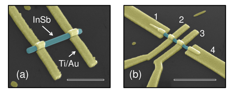
Figures 1a and 1b show false-color coded SEM images of a two-probe and a four-probe InSb NWFET. In the measurements for the two-probe device (Figure 1a), a dc voltage is applied between the source (S) and the drain (D) electrode, and the current is recorded with the same electrodes. In this case, it is inevitable that part of the applied voltage drops at the two contacts, with each characterized by a contact resistance . The measured resistance is given by , where the contact resistances at the two contacts are assumed to be the same and is the resistance of the NW channel. While in the measurements for the four-probe device (Figure 1b), a dc current is applied to the NW through the two outer electrodes 1 and 4, and the voltage drop between the two inner probes 2 and 3 is recorded. In this way, the measured resistance, , reflects mostly the NW channel resistance and thus the four-probe measurement method provides a direct measure of the channel transport properties.
3 Results and discussion
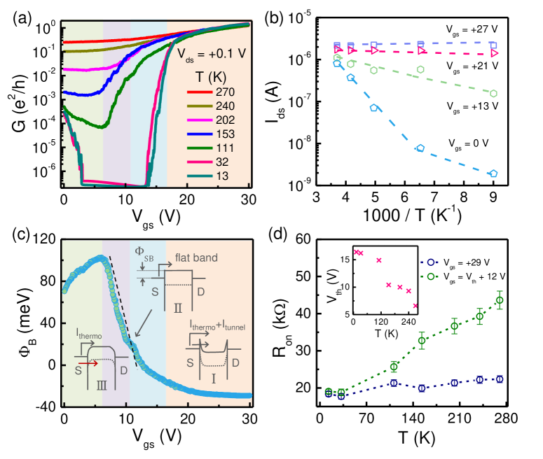
Figure 2 shows the transfer characteristics of the device shown in Figure 1a (Device 1) measured in the two-probe configuration at different temperatures and the extracted SB height at the metal-InSb NW interfaces. Here the device has a large contact spacing and thus operates in the diffusive regime. Figure 2a shows the two-probe conductance of the device, obtained by dividing the measured S-D current by , as a function of the applied gate voltage at different temperatures (). The measurements were performed at a constant V. The flat-band voltage and the threshold voltage of this device at K are 11 V and 16.4 V , respectively. As shown in the figure, at high temperatures, the device shows a high off-state conductance and a low on/off conductance ratio. At temperatures below 150 K, the device shows an asymmetric ambipolar behavior. This is a typical signature of a narrow band gap NWFET [39]. As has been discussed by Appenzeller et al. [21], the presence of SBs affects largely the transport characteristics of a NWFET device in the gate voltage region close to the pinch-off threshold. For , the injecting current consists of a thermionic emission component and a direct tunneling component (see Figure 2c, inset I). For , it is the thermally-assisted tunneling through the barrier that dominantly modifies the current injection. The crossover from a tunneling-modified to a thermionic emission-dominated process occurs at the flat-band condition, (Figure 2c, inset II). As continuously decreasing , the thermionic emission over the barrier becomes the main, if not only, access for current injection. To extract the true , the transfer curves in Figure 2a are converted to the Arrhenius plots at different gate voltages shown in Figure 2b. The data at high temperatures can then be fitted to a classical thermionic emission equation, to extract the effective barrier height , as
| (1) |
where is the Richardson constant, is the Boltzmann constant, and is the elementary charge. The results are shown in Figure 2c. It is seen that the extracted is modulated by . Based on the above band alignment analysis, is linearly related to as for , where is a voltage scaling factor. We extract a Schottky barrier height of from the flat-band condition. Note that eq (1) works only for a single barrier case. Considering the small extracted, the applied +0.1 V S/D bias is large enough to eliminate the SB at the drain contact, while avoids possible band-to-band tunneling current injection at higher biases. As is continuously decreased, shows a decrease as seen in the left-side region of Figure 2c. This can be understood as the emergence of hole current, as denoted by a red arrow in the inset III of Figure 2c, when the Fermi level is positioned close to the valence band. Accordingly, reaches a maximum when the Fermi level at the metal contact is in lineup with the middle of the band gap. This simple scenario yields an approximate upper-bound value of the NW band gap . We should note that the extracted values of become negative at the on state of the device as shown in Figure 2c, which indicates that the method for extraction of is no longer applicable for the device at on state. The negative values of arise from the fact that at on state, the contact resistance of the NWFET is relatively small and the measured temperature dependence of the current in the two-probe configuration is dominantly induced by the change of the nanowire resistance with varying temperature. To see this, we show in Figure 2d the measured on-state resistance of the device with decreasing temperature. The data points in green circles are extracted by taking into account a -dependent shift of the threshold voltage as shown in the inset of Figure 2d and setting at values of 12 higher than . As a comparison, the values measured at a fixed high value of =29 ) are also plotted in Figure 2d as blue circles. In both cases, show an overall decrease with decreasing temperature, which is seldom investigated in SB height extraction experiments [21, 38, 46]. The decrease of , or equivalently the increase of , with lowering has been reported before in InAs NWFETs in both the ballistic and the diffusive transport regime [47, 48] and can be explained by suppression of phonon scattering at low temperatures.
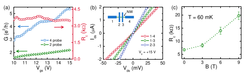
Now we turn to consider the contact resistance at the Ti/Au-InSb NW interfaces. We can reliably extract the contact resistance from measurements of a four-probe device as shown in Figure 1b at low temperatures [49]. Figure 3a shows the results of the measurements for a typical four-probe device (Device 2) at on state at . In these measurements, a two-probe trace is first recorded using the two inner electrodes 2 and 3, while keeping the two outer electrodes 1 and 4 floated (cf. Figure 1b or the inset of Figure 3b). Then a four-probe trace is taken by applying a constant current using electrodes 1 and 4. The contact resistance can be determined from the measured two-probe and four-probe conductance according to , where and represent the two-probe and the four-probe conductance, respectively. For Device 2 at on state, is around 2 times of , giving an average contact resistance of and a normalized value of (normalized to the NW circumference). Altogether, three four-probe devices are measured and it is found that shows device-to-device variations in a range of . It is worthwhile to note that at on state, the measured characteristics of our devices all show good ohmic behaviors. An example is shown in Figure 3b, where the characteristics of Device 2 at on state measured using different combinations of two probes at are presented. Here, it is seen that all the measured curves are linear and ohmic like.
To analyze the physical origin of the contact resistance of InSb NWFETs at low temperatures, we carry out the magnetotransport measurements and examine the effect of magnetic field on the extracted of our devices. Figure 3c shows the magnetic field dependence of measured for a four-probe device (Device 3) at on state. Here, the magnetic field is applied perpendicular to the substrate and each value is obtained by averaging over a range of at on state with standard errors indicated by vertical bars. Interestingly, develops a pronounced upturn at high fields. The transition to the upturn in the curve can be roughly estimated to occur around . To understand this transition, we consider qualitatively the response of the band structure of the NW to a change in the applied magnetic field. Generally, the contact resistance contains two terms, and . The first term, , comes from the potential barrier at the metal-NW interface and is sample-dependent due to specific interface properties. The second term, , is due to the mode mismatch between three-dimensional electron states in the metal and quasi-one-dimensional subband states in the semiconductor NW. At on state, it is reasonably assumed that the Schottky barrier at the metal-semiconductor NW interface is very thin and is transparent for electron conduction. Thus, can be neglected and we have approximately for the NWFET at on state at low temperatures. Under this condition, can be analyzed based on the well-known Landauer formula, , where is the number of conduction modes, is the transmission coefficient of each mode, and is the Planck constant [22]. We have estimated, from the low-temperature transfer characteristics of the device, the electron mean free path in the NW is about , which is much smaller than the spacing of between the probes. Thus, our device is in the quasi-ballistic or the diffusive transport regime. Yet, the quantized conductance have been reported in InSb [43] and InAs [47] NWs with contact spacings several times larger than the mean free path, no such signatures have been observed in the devices reported here. Nevertheless, the transport in our devices is still sensitively dependent on the magnetoelectric subbands in the NW at an applied magnetic field. As the field is increased, various features are expected to appear, such as a larger subband separation, flattening of the energy band inside the NW, and successive depopulation of the magnetoelectric subbands [50, 51, 52]. In the context of transport, the depopulation of the magnetoelectric subbands amounts to a fall in the number of conducting channels below the Fermi level at high magnetic fields, or equivalently, the occurrence of upturn in the contact resistance as observed in our experiment. The relevant length scale for the onset of the magnetic field dependence of is the cyclotron orbit radius , which can be estimated from the form of , where is the Fermi wavevector and is the magnetic length with being the reduced Planck constant. When the cyclotron orbit radius becomes or smaller at high magnetic field, the Landau levels are formed in the inside of the NW and the magnetoelectric subbands bend up at the NW boundary, leading to the formation of edge state channels [53]. As a consequence, both the channel mobility in the NW can be increased due to the suppression of back scattering and the contact resistance can be increased due to the depopulation of magnetoelectric subbands. The above analysis gives the estimation for the onset field , at which the contact resistance starts to increase with increasing magentic field, as
| (2) |
For Device 3, using the determined from the transfer characteristics, an onset field of can be deduced, which is close to the measured value of .
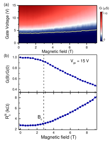
To further support the scenario of the magnetic depopulation of subbands in InSb NWs, we carried out magnetoconductance measurements on another two-probe device (Device 4). Figure 4a shows the measured conductance of the device as a function of and . The yellow line in the figure denotes the threshold gate voltage at which the NW channel is open for conduction. It is evident that the threshold gate voltage is increased with increasing . The upper panel of Figure 4b shows the measured conductance (normalized to the conductance at ) of the device at on state as a function of . Here, an overall descending trend of the conductance with increasing magnetic field is seen. This seems at first sight counter-intuitive given the fact that the introduction of a magnetic field suppresses back scattering in the NW and thus leads to an increase in the channel mobility. Indeed, Dhara et al. observed a mobility increase in the magnetotransport measurements of InAs NWs [54]. In our case, however, because of the presence of the contact resistance, the field-effect mobility can not be directly extracted from two terminal measurements with the expression , where is the maximum transconductance, is the contact spacing and is the gate-to-nanowire capacitance per unit length [55]. Instead, we need to adopt the method reported by Gül et al. [44] by incorporating into the expression of the conductance as follows,
| (3) |
Here , , and are free fitting parameters. In analysis of our measured results, we assume that is magnetic field dependent and is independent of the magnetic field, i.e., neglecting the effect of the increases in with increasing magnetic field. The lower panel in Figure 4b shows the result of obtained by fitting the measured data shown in Figure 4a to the above expression as a function of . Strikingly, we noticed a shared feature for the two panels—both the normalized conductance and the extracted contact resistance first undergo an initial stage with small variations and then start to decrease or increase quickly after , a magnetic field value which is very close to the onset field deduced for this device (dashed line). This consistency is not a coincidence but reveals unambiguously the critical role of the contact resistance arising from mode mismatching. The significant rise in after the applied magnetic field is stronger than provides a strong hint on the subband structure modulation by the magnetic field and thus supports our proposed dominant physical origin of the contact resistance of InSb NWFETs at on state at low temperatures.
4 Conclusions
In conclusion, we have carried out an experimental study of Ti/Au-contacted InSb NWFETs with two-probe and four-probe designs and have extracted the Schottky barrier height and contact resistance at the Ti/Au-InSb NW interfaces. We have shown that a Schottky barrier height of is present at the Ti/Au-InSb NW interfaces and the effective barrier height is gate tunable. We have also demonstrated that the contact resistance of the devices at on-state arises dominantly from mode mismatching between the electron states in the contact metal and the semiconductor NWs and is magnetic field dependent. The significant increase of after an onset magnetic field is interpreted as due to the magnetic depopulation of the subbands in the NWs and the onset field strength can be estimated simply by setting the electron cyclotron radius to a half of the NW diameter. Our finding of a variable effective Schottky barrier height points to readily feasible device designs, where the injection barrier can be tuned by local gates, aiming at both applications and fundamental research.
References
References
- [1] Colinge J P, Lee C W, Afzalian A, Akhavan N D, Yan R, Ferain I, Razavi P, O’Neill B, Blake A, White M, Kelleher A M, McCarthy B and Murphy R 2010 Nat. Nanotechnol 5 225–229
- [2] Riel H, Wernersson L E, Hong M and del Alamo J A 2014 MRS Bull. 39 668–677
- [3] Sze S M and Ng K K 2007 Physics of Semiconductor Devices 3rd ed (Hoboken NJ: John Wiley & Sons)
- [4] Léonard F and Talin A A 2011 Nat. Nanotechnol 6 773–783
- [5] Dey A W, Thelander C, Lind E, Dick K A, Borg B M, Borgström M, Nilsson P and Wernersson L E 2012 IEEE Electron Device Lett. 33 791–793
- [6] Lu K C, Wu W W, Wu H W, Tanner C M, Chang J P, Chen L J and Tu K N 2007 Nano Lett. 7 2389–2394
- [7] Chen Y, Lin Y C, Huang C W, Wang C W, Chen L J, Wu W W and Huang Y 2012 Nano Lett. 12 3115–3120
- [8] Chen Y, Lin Y C, Zhong X, Cheng H C, Duan X and Huang Y 2013 Nano Lett. 13 3703–3708
- [9] Weber W M, Geelhaar L, Graham A P, Unger E, Duesberg G S, Liebau M, Pamler W, Chèze C, Riechert H, Lugli P and Kreupl F 2006 Nano Lett. 6 2660–2666
- [10] Wu Y, Xiang J, Yang C, Lu W and Lieber C 2004 Nature 430 61–65
- [11] Larson J M and Snyder J P 2006 IEEE Trans. Electron Devices 53 1048–1058
- [12] Appenzeller J, Knoch J, Riel H, Schmid H and Riess W 2008 IEEE Trans. Electron Devices 55 2827–2845
- [13] Mongillo M, Spathis P, Katsaros G, Gentile P and Franceschi S D 2012 Nano Lett. 12 3074–3079
- [14] Heinzig A, Slesazeck S, Kreupl F, Mikolajick T and Weber W M 2012 Nano Lett. 12 119–124
- [15] Heinzig A, Mikolajick T, Trommer J, Grimm D and Weber W M 2013 Nano Lett. 13 4176–4181
- [16] Glassner S, Zeiner C, Periwal P, Baron T, Bertagnolli E and Lugstein A 2014 Nano Lett. 14 6699–6703
- [17] Freitag M, Radosavljevic M, Zhou Y, Johnson A T and Smith W F 2001 Appl. Phys. Lett. 79 3326–3328
- [18] Martin D, Heinzig A, Grube M, Geelhaar L, Mikolajick T, Riechert H and Weber W M 2011 Phys. Rev. Lett. 107 216807
- [19] Heinze S, Tersoff J, Martel R, Derycke V, Appenzeller J and Avouris P 2002 Phys. Rev. Lett. 89 106801
- [20] Appenzeller J, Knoch J, Derycke V, Martel R, Wind S and Avouris P 2002 Phys. Rev. Lett. 89 126801
- [21] Appenzeller J, Radosavljević M, Knoch J and Avouris P 2004 Phys. Rev. Lett. 92 048301
- [22] Datta S 1995 Electron Transport in Mesoscopic Systems 1st ed (Cambridge, England: Cambridge University Press)
- [23] van Wees B J, van Houten H, Beenakker C W J, Williamson J G, Kouwenhoven L P, van der Marel D and Foxon C T 1988 Phys. Rev. Lett. 60 848–850
- [24] Wharam D A, Thornton T J, Newbury R, Pepper M, Ahmed H, Frost J E F, Hasko D G, Peacock D C, Ritchie D A and Jones G A C 1989 J. Phys. C: Solid State Phys. 21 L209–L214
- [25] de Picciotto R, Stormer H L, Pfeiffer L N, Baldwin K W and West K W 2001 Nature 411 51–54
- [26] Borg B M and Wernersson L E 2013 Nanotechnology 24 202001
- [27] Nilsson H A, Deng M T, Caroff P, Thelander C, Samuelson L, Wernersson L E and Xu H Q 2012 IEEE J. Sel. Top. Quantum Electron. 4 8
- [28] Nilsson H A, Caroff P, Thelander C, Larsson M, Wagner J B, Wernersson L E, Samuelson L and Xu H Q 2009 Nano Lett. 9 3151–3156
- [29] Nadj-Perge S, Pribiag V S, van den Berg J W G, Zuo K, Plissard S R, Bakkers E P A M, Frolov S M and Kouwenhoven L P 2012 Phys. Rev. Lett. 108(16) 166801
- [30] Fan D, Li S, Kang N, Caroff P, Wang L B, Huang Y Q, Deng M T, Yu C L and Xu H Q 2015 Nanoscale 7(36) 14822–14828
- [31] Mourik V, Zuo K, Frolov S M, Plissard S R, Bakkers E P A M and Kouwenhoven L P 2012 Science 336 1003
- [32] Deng M T, Yu C L, Huang G Y, Larsson M, Caroff P and Xu H Q 2012 Nano Lett. 12 6414–6419
- [33] Churchill H O H, Fatemi V, Grove-Rasmussen K, Deng M T, Caroff P, Xu H Q and Marcus C M 2013 Phys. Rev. B 87(24) 241401
- [34] Deng M T, Yu C L, Huang G Y, Larsson M, Caroff P and Xu H Q 2014 Sci. Rep. 4 7261
- [35] van den Berg J W G, Nadj-Perge S, Pribiag V S, Plissard S R, Bakkers E P A M, Frolov S M and Kouwenhoven L P 2013 Phys. Rev. Lett. 110(6) 066806
- [36] Noguchi M, Hirakawa K and Ikoma T 1991 Phys. Rev. Lett. 66(17) 2243–2246
- [37] Olsson L O, Andersson C B M, Håkansson M C, Kanski J, Ilver L and Karlsson U O 1996 Phys. Rev. Lett. 76(19) 3626–3629
- [38] Razavieh A, Mohseni P K, Jung K, Mehrotra S, Das S, Suslov S, Li X, Klimeck G, Janes D B and Appenzeller J 2014 ACS Nano 8 6281–6287
- [39] Zhao Y, Candebat D, Delker C, Zi Y, Janes D, Appenzeller J and Yang C 2012 Nano Lett. 12 5331–5336
- [40] Nilsson H A, Caroff P, Thelander C, Lind E, Karlström O and Wernersson L E 2010 Appl. Phys. Lett. 96 153505
- [41] Wang Y, Chi J, Banerjee K, Grützmacher D, Schäpers T and Lu J G 2011 J. Mater. Chem. 21 2459–2462
- [42] Yao H, Günel H Y, Blömers C, Weis K, Chi J, Lu J G, Liu J, Grützmacher D and Schäpers T 2012 Appl. Phys. Lett. 101 082103
- [43] van Weperen I, Plissard S R, Bakkers E P A M, Frolov S M and Kouwenhoven L P 2012 Nano Lett. 13 387–391
- [44] Gül Ö, van Woerkom D J, van Weperen I, Car D, Plissard S R, Bakkers E P A M and Kouwenhoven L P 2015 Nanotechnology 26 215202
- [45] Suyatin D B, Thelander C, Björk M T, Maximov I and Samuelson L 2007 Nanotechnology 18 105307
- [46] Das S, Chen H Y, Penumatcha A V and Appenzeller J 2013 Nano Lett. 13 100–105
- [47] Chuang S, Gao Q, Kapadia R, Ford A C, Guo J and Javey A 2013 Nano Lett. 13 555–558
- [48] Wang L, Guo J, Kang N, Pan D, Li S, Fan D, Zhao J and Xu H Q 2015 Appl. Phys. Lett. 106 173105
- [49] Mohney S, Wang Y, Cabassi M, Lew K, Dey S, Redwing J and Mayer T 2005 Solid-State Electron. 49 227–232
- [50] Knobbe J and Schäpers T 2005 Phys. Rev. B 71 035311
- [51] Nanot S, Avriller R, Escoffier W, Broto J M, Roche S and Raquet B 2009 Phys. Rev. Lett. 103 256801
- [52] Vigneau F, Prudkovkiy V, Duchemin I, Escoffier W, Caroff P, Niquet Y M, Leturcq R, Goiran M and Raquet B 2014 Phys. Rev. Lett. 112 076801
- [53] Royo M, Bertoni A and Goldoni G 2013 Phys. Rev. B 87 115316
- [54] Dhara S, Solanki H S, Singh V, Narayanan A, Chaudhari P, Gokhale M, Bhattacharya A and Deshmukh M M 2009 Phys. Rev. B 79(12) 121311
- [55] Dayeh S A, Aplin D P R, Zhou X, Yu P K L, Yu E T and Wang D 2007 Small 3 326–332