Conductivity fluctuations in proton-implanted ZnO microwires
Abstract
The electric noise can be an important limitation for applications of conducting elements of size in the nanometer range. The intrinsic electrical noise of prospective materials for opto-spintronics applications like ZnO has not been characterized yet. In this study we have investigated the conductivity fluctuations in 10 nm thick current paths produced by proton implantation of ZnO microwires at room temperature. The voltage noise under a constant dc current bias in undoped as well as in Li-doped microwires is characterized by power spectra with . The noise intensity scales with the square of the bias current pointing out to bias-independent resistivity fluctuations as a source of the observed noise. The normalized power spectral density appears inversely proportional to the number of carriers in the probed sample volume, in agreement with the phenomenological Hooge law. For the proton-implanted ZnO microwire and at 1 Hz we obtain a normalized power spectral density as low as Hz-1.
pacs:
72.70.+m,78.67.Uh,61.82.Fk1 Introduction
The quest for further reduction of the components’ size of electronic devices can be seriously limited by an increase of the electric noise, particularly in metallic nanowires [1]. However, the phenomenon of defect-induced magnetism (DIM), i.e., magnetic order produced by defects and/or added ions (not necessarily magnetic) in the atomic lattice of oxides and other materials, indirectly requires a pronounced sample size reduction [2, 3, 4, 5, 6, 7, 8]. Due to the O-2 hole-spin polarization from oxygen atoms around Zn-vacancies in ZnO[9, 10], the DIM phenomenon opens up new possibilities for spintronics applications of the ZnO compound. Due to the very nature of DIM and the difficulties in creating an adequate density of defects that would be homogeneously distributed all over the entire volume of an oxide sample, different experimental strategies were used to obtain large ferromagnetic magnetization values at saturation. These include, for example, ion irradiation [5, 11], co-doping, [12, 13, 10] and sample size reduction [10, 14]. By implantation of protons at energy eV one can obtain a magnetically ordered nm thick surface regions in ZnO:Li microwires. These regions show clear ferromagnetic characteristics, as revealed by SQUID magnetometry and x-ray magnetic circular dichroism (XMCD)[10] as well as a negative magnetoresistance [14]. Therefore, increase of the noise associated with decrease of the effective size of the magnetically ordered sample volume may become a limiting factor for the applications of magnetic oxide nanowires in spintronics.
Let us underline that the electric noise measurements reported so far for ZnO nanowires were performed using nanowires incorporated into field effect transistor structures[15, 16]. For this reason and in most cases, such measurements do not necessarily reveal the intrinsic noise of the nanowires but rather the dominating interfaces and contacts contributions. The main aim of the experimental work we report in this letter is the investigation of the intrinsic conductivity noise spectra of ZnO microwires implanted with protons, in which basically only a very thin, nanorange sized surface layer of the wire conducts the electricity.
We have investigated the transport noise properties of two ZnO microwires at room temperature. The first ZnO wire is doped with Li and shows magnetic order at room temperatures after proton implantation [10]. For comparison, a second ZnO wire without Li doping but with a similar proton implantation dose as the first one, has also been measured. This latter wire does not show any magnetic order at room temperature[14]. Both microwires are characterized by -like noise. Its intensity is several orders of magnitude smaller than that reported for ZnO nanowires in field effect transistors[15, 16] and purely Gaussian statistical properties.
2 Experimental details
Clean and Li-doped () ZnO powders were obtained by thermal decomposition of Zinc Acetate. As starting precursors Zinc Acetate dihydrate Zn(CH3COO) 2H2O and Li-hydroxide mono hydrate LiOH H2O of (Sigma-Aldrich) (99.99%) commercial chemicals were used. The precursors were mixed in 30 ml of tri-distilled water at a nominal concentration of 3 at.% Li/Zn. The obtained wires, i.e. pure ZnO and Li-doped ZnO showed wurzite like structure with hexagonal morphology with the c-axis as main wire growth axis. Further details of the microwire preparation can be taken from Refs. [10, 17].
The size of the two wires were: (diameter length between the voltage measuring electrodes) m2 for the ZnO microwire (ZnO) and m2 for the Li-doped ZnO nanowire (LiZnO), see Fig. 1. The pure and the Li-doped wires were exposed to remote H+ DC plasma ( eV H+ implantation energy) in the parallel-plate configuration (60 A bias current for one hour at a chamber pressure of 0.5 mbar) using a procedure described in Refs. [18, 19]. The ZnO wire was electrically contacted with indium electrodes after the entire wire was proton irradiated. The indium contacts were necessary because the large diameter of the wire hindered simple lithographic contacts. No annealing was necessary and the ohmic behavior was checked before we started the noise measurements. In the case of the Li:ZnO nanowire the proton implantation and the contacts were performed in two steps. Firstly, the contact paths were done with electron lithography and the proton implantation of the contact regions was carried out, previous to any metal deposition. Afterwards, the Pd/Au electrical contacts were deposited by sputtering on the electrode paths. Following this procedure the electrical contacts always showed good ohmic behavior. Finally, the proton implantation on the rest of the wire was performed. This procedure was necessary to avoid any diffusion of H+ during the lithography process.
The resistivity of the wires after H+ implantation at 300 K were cm (cm) for H:LiZnO (H:ZnO), several orders of magnitude smaller than before implantation. All Li-doped ZnO microwires are highly insulating with a resistance larger than at room temperature [14]. At the energy used for implantation of H+ in our samples, a significant concentration of protons as well as defects (Zn- and O-vacancies) are localized only within a nm surface region according to SRIM simulations [20] (see also Fig. 1 in [18]). The defects concentration (Zn-vacancies) is important for the magnetism [10, 14]. In fact, it was experimentally verified that most of the magnetic signal comes from the near surface region [18]. The temperature dependence of the resistance can be understood using a simple parallel resistor model that takes into account two contributions to the total conduction, one from the near surface region and the other from a non-magnetic region further inside the wire, where a lower H+ doping also reduces, but in a minor grade, the resistance [14]. Transport studies of H+-implanted ZnO single crystals [21] and microwires [22] indicate that the metallic-like contribution is associated with the hydrogen-rich near surface region of the samples. The photoluminescence spectra at 300 K and the magnetic properties (SQUID, XMCD and magnetoresistance) of the wires have been reported recently [10, 14].
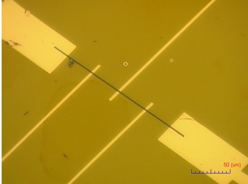
The conductivity noise was measured at room temperature by biasing the samples with dc current, supplied by high output impedance current source, and recording the resulting voltage fluctuations. Due to the very high resistances of the wires we have employed a five-point contacts arrangement to reduce the dc voltage drop on the current biased sample, see Fig. 1. In this contact arrangement the current flows from the two most external contacts to the grounded collector contact located at the middle of the sample, between the two internal contacts across which the fluctuating voltage is measured, see Fig. 1. The voltage drop across the dc current biased wire was amplified by a homemade very low noise preamplifier and processed by a computer-assisted digital signal analyzer. The 5-contacts arrangement allowed us to avoid problems associated with preamplifier input saturation or with exceeding the common mode rejection capability for all used input dc currents within the range A A. To eliminate environmental interferences and noise background, along with each measurement the power spectral density (PSD) at zero current was measured separately and subtracted afterwards from the PSD obtained at a given current flow, providing us the pure PSD of the intrinsic sample fluctuations.
3 Results and discussion
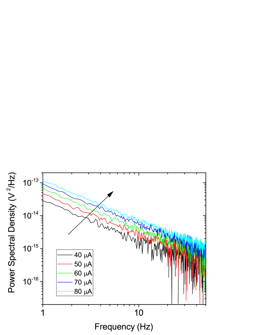
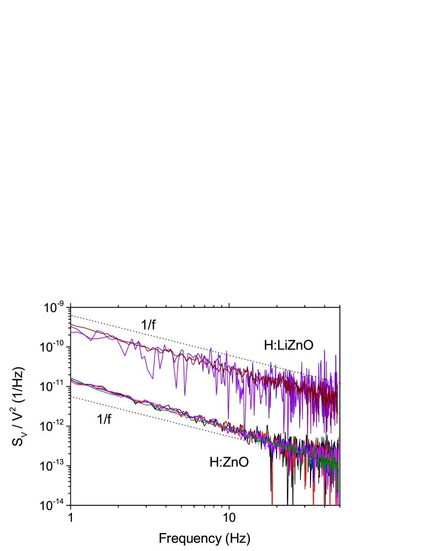
Figure 2 shows a set of averaged PSD recorded at different current dc current flow in the H:ZnO microwire. The spectra demonstrate a frequency dependence of the type with the exponent . The intensity of the noise increases with increasing bias current. Voltage noise with a spectrum is generally related to resistance fluctuations, which are measured by applying dc current and recorded as voltage fluctuations. When the resistance fluctuations are just probed by current, and are not influenced by its flow, then PSD of the voltage noise scales as the square of the bias current. Such modulation noise is frequently referred to as quasi-equilibrium noise. Figure 3 shows PSD recorded under different current flows and normalized by the square of the dc voltage across the wire. For both samples, the normalized PSD collapses to a single line indicating that PSD scales with the square of the bias, meaning that the current flow does not excite or influence these auscultations but only reveals them by converting conductivity fluctuations into the measurable voltage noise. Consequently, , where is the measured PSD of voltage fluctuations and is the PSD of the underlying conductivity noise.
The measured noise does not depend on weak, of the order of few hundredths of Gauss, applied magnetic field and on illumination of the wires with UV light. This is not surprising for the undoped H:ZnO wire because it is not magnetically ordered at room temperature [14]. For the magnetic one [10] the hysteresis loops with a finite width indicate either finite pinning of domain walls and/or some unknown magnetic anisotropy. With an applied field of the order of 0.5 kOe it is possible to change the magnetization notably, probably due to the reduction of the number of domains. The domain walls move back and forth at room temperature, especially if there are AC magnetic fields or currents applied to the wire. Any driven force would change locally the magnetization and this might constitute a source of additional Barkhausen-like noise. The frequency spectrum of this noise can be very broad, up to the MHz region. Our study and the negligible effect of the applied magnetic field on the measured noise indicates that its source is not related to the magnetic order of the sample.
The increase in the number of carriers under UV light illumination at room temperatures is small because both wires are implanted with protons resulting in the resistance of the implanted sections being much smaller that the resistance of the untreated parts of the wire, which is most sensitive to the UV light illumination. Because of this, most of the bias current is shunted to the lower resistance part, which is only weakly influenced by the light, with a relative decrease of the total resistance under UV of the order of 10% to 30%. The UV effect on the electrical noise is therefore negligible. The absence of any increase of the noise under UV is relevant for the detection of defect-induced magnetic order in low-dimensional ZnO structures [23].
There is, however, a noticeable difference in the noise intensity between the H:LiZnO and H:ZnO wires. The normalized noise, which is insensitive to the actual value of the sample resistance, is 25 times higher in the H:LiZnO sample than in the H:ZnO. Moreover, the PSD of the H:LiZnO wire is very close to the ideal noise. The spectral exponent obtained by fitting the experimental spectra to form is , while the spectral exponent of the H:ZnO wire noise is higher, . Observe that the difference in the exponent is well beyond the experimental uncertainty of the measurements.
To understand the difference in the spectral properties of both samples we have to recall the widely accepted nonexponential kinetics model for noise in solids[24]. According to this model, noise results from incoherent superposition of many elementary random two-level fluctuators (TLF), each producing a Lorentzian contribution with a single relaxation time . The overall spectrum of a system is due to incoherent superposition of contributions of all individual TLFs, and depends on the distribution of the relaxation times in the system. When the distribution , then the integrated spectrum becomes pure noise . Assuming that the TLFs are thermally activated, what in our case of the room temperature experiment is quite obvious, we write for , where is the attempt frequency, usually related to the phonon frequency in solids and is the activation energy in a symmetric TLF. The resulting total noise spectrum of an ensemble of active TLFs, given by
| (1) |
has a pure form for Therefore, the slope of the PSD function, i.e., the spectral exponent , reflects the shape of the energy distribution within the experimentally accessible energy window. A departure of the spectral slope from implies a deviation of the energy distribution from a flat one. In particular, a spectral slope with implies an excess in the density of the low energy fluctuators in the system. Therefore, the distribution of energy barriers of the scatterers in the H:LiZnO wire where is very close to unity is flat, while that of the H:ZnO wire with is skewed in such a way that there is an excess of scatterers at low energies. The reason for such a difference can be intuitively understood remembering that the introduction of protons to ZnO suppresses severely the formation of compensating interstitials and enhances the acceptor solubility in ZnO by forming H-acceptor complexes and leading to enhanced conductivity[25]. On the other hand, doping with Li stabilizes and bounds hydrogen in the H:LiZnO structure while in H:ZnO crystal the hydrogen is not bonded and diffuses freely towards the surface and the interior. Therefore, the distribution of hydrogen in the H:LiZnO is uniform resulting in a flat distribution of activation energies while in H:ZnO the areas close to the surface or at the interface with the insulating part are enriched with hydrogen and have lower activation energies than the remaining H-implanted parts of the wire resulting in a skewed distribution of activation energies and consequently the spectral exponent .
The difference in the normalized noise magnitude between the wires can be ascribed to difference in number of charge carriers in the effective volumes from which the noise has been measured. The conductivity fluctuations in many solid state systems can be quantified by a phenomenological Hooge equation ( is a constant) indicating that the normalized noise at 1 Hz should scale inversely proportional to the number of carriers [24]. One can evaluate the ratio of the number of carriers in the wires as (subindex 1 for H:LiZnO and 2 for H:ZnO) from the ratio of the measured resistances of both wires , using the simple Drude model in which the resistivity , where is an effective mass of charge carriers, their charge, the mean time a charge carrier has traveled since the last collision (the relaxation time), carrier concentration and is the probed volume of the sample. The resistance of the sample reads , where is the distance between the contacts and the cross-section area of the wire. From the last expression and considering similar effective masses for both wires we have
| (2) |
With the experimental values =11.3 and =25 one obtains
| (3) |
Assuming that the noise intensity ratio properly reflects the ratio of number of carriers in the active volumes of the two samples, to keep the consistency between the estimations one has to assume that . This appears to be a reasonable assumption taking into account the measured resistivities, the expected similar carrier densities in the two wires (due to similar proton doses), and the Matthiesen rule where . Due to the Li doping, which increases the pinning of protons and Zn vacancies near Li ions, we expect a clear decrease of for the Li doped wire respect to the undoped one.
In conclusion, we have measured the intrinsic noise spectra of proton implanted ZnO and Li:ZnO wires with a 10 nm thick conducting surface layer. The spectral density follows basically a dependence with an exponent close to 1 for the H:LiZnO wire. For the wire H:ZnO, however, the exponent , which can be attributed to a non-constant distribution of activation energies of the fluctuators assembly. The consistency between the resistivity ratio of the doped and undoped wires and the ratio of the normalized noise intensity allows one to conclude that the relaxation time in Li-doped ZnO microwires is an order of magnitude shorter with respect to undoped samples. The intensity of the normalized intrinsic microwire noise observed in our experiments Hz-1, orders of magnitude smaller than the reported for ZnO nanowires in field effect transistor configurations[15, 16]. Therefore, it is clear that in the latter configuration the observed noise is dominated by extrinsic contacts and interface contributions.
Acknowledgments: This work was funded by the Collaborative Research Center SFB 762 “Functionality of Oxide Interfaces” in Germany.
References
References
- [1] Bid A, Bora A and Raychaudhuri A K 2006 Nanotechnology 17 152
- [2] Peng H, Xiang H J, Wei S H, Li S S, Xia J B and Li J 2009 Phys. Rev. Lett. 102(1) 017201
- [3] McCluskey M D and Jokela S J 2009 Journal of Applied Physics 106 071101
- [4] Xing G Z, Lu Y H, Tian Y F, Yi J B, Lim C C, Li Y F, Li G P, Wang D D, Yao B, Ding J, Feng Y P and Wu T 2011 AIP Advances 1 022152
- [5] Esquinazi P, Hergert W, Spemann D, Setzer A and Ernst A 2013 IEEE TRANSACTIONS ON MAGNETICS 49 4668
- [6] Guglieri C, Céspedes E, Espinosa A, Laguna-Marco M A, Carmona N, Takeda Y, Okane T, Nakamura T, García-Hernández M, García M A and Chaboy J 2014 Advanced Functional Materials 24 2094–2100
- [7] Kenmochi K, Dinh V A, Sato K, Yanase A and Katayama-Yoshida H 2004 Journal of the Physical Society of Japan 73 2952–2954
- [8] Katayama-Yoshida H, Sato K, Fukushima T, Toyoda M, Kizaki H, Dinh V A, and Dederichs P H 2007 Phys. Stat. Sol. (a) 204 15–32
- [9] Yi J B, Lim C C, Xing G Z, Fan H M, Van L H, Huang S L, Yang K S, Huang X L, Qin X B, Wang B Y, Wu T, Wang L, Zhang H T, Gao X Y, Liu T, Wee A T S, Feng Y P and Ding J 2010 Phys. Rev. Lett. 104 137201
- [10] Lorite I, Straube B, Ohldag H, Kumar P, Villafuerte M, Esquinazi P, Rodríguez Torres C E, Perez de Heluani S, Antonov V N, Bekenov L V, Ernst A, Hoffmann M, Nayak S K, Adeagbo W A, Fischer G and Hergert W 2015 Applied Physics Letters 106 082406
- [11] Zhou S 2014 Nuclear Instruments and Methods in Physics Research B 326 55
- [12] Herng T S, Qi D C, Berlijn T, Yi J B, Yang K S, Dai Y, Feng Y P, Santoso I, Sánchez-Hanke C, Gao X Y, Wee A T S, Ku W, Ding J and Rusydi A 2010 Phys. Rev. Lett. 105 207201
- [13] Yi J B, Lim C C, Xing G Z, Fan H M, Van L H, Huang S L, Yang K S, Huang X L, Qin X B, Wang B Y, Wu T, Wang L, Zhang H T, Gao X Y, Liu T, Wee A T S, Feng Y P and Ding J 2010 Phys. Rev. Lett. 104 137201
- [14] Lorite I, Zandalazini C, Esquinazi P, Spemann D, Friedl nder S, Pöppl A, Michalsky T, Grundmann M, Vogt J, Meijer J, Heluani S P, Ohldag H, Adeagbo W A, Nayak S K, Hergert W, Ernst A and Hoffmann M 2015 J. Phys.: Condens. Matter 27 256002
- [15] Xiong H D, Wang W, Suehle J S, Richter C A, Hong W K and Lee T 2008 Journal of Nanoscience and Nanotechnology 8 1
- [16] Ju S, Kim S, Mohammadi S, Janes D B, Ha Y G, Facchetti A and Marks T J 2008 Appl. Phys. Lett. 92 022104
- [17] Villafuerte M, Ferreyra J M, Zapata C, Barzola-Quiquia J, Iikawa F, Esquinazi P, Heluani S P, de Lima M M and Cantarero A 2014 Journal of Applied Physics 115 133101
- [18] Khalid M, Esquinazi P, Spemann D, Anwand W and Brauer G 2011 New Journal of Physics 13 063017
- [19] Lorite I, Esquinazi P, Zapata C and Heluani S P 2013 Journal of Materials Research 29 78–83
- [20] Ziegler J F, Biersack J P and Ziegler M D 2008 SRIM - The Stopping and Range of Ions in Matter (SRIM Co.) ISBN 0-9654207-1-X. See also the simulation software IIS available at http://www.ele.uva.es/ jesman/iis.html, which has some advantages in comparison with the usual SRIM simulation.
- [21] Khalid M and Esquinazi P 2012 Phys. Rev. B 85 134424
- [22] Lorite I, Esquinazi P, Zapata C and Heluani S P 2014 J. Mater. Res. 29(01) 78–83 ISSN 2044-5326
- [23] Lorite I, Kumar Y, Esquinazi P, Zandalazini C and de Heluani S P 2015 Small 11 4403–4407
- [24] Weissman M B 1998 Rev. Mod. Phys. 60 537
- [25] Eun-Cheol L and Chang K J 2004 Phys. Rev. B 70 115210