Nanosecond-timescale spin transfer using individual electrons in a quadruple-quantum-dot device
Abstract
The ability to coherently transport electron-spin states between different sites of gate-defined semiconductor quantum dots is an essential ingredient for a quantum-dot-based quantum computer. Previous shuttles using electrostatic gating were too slow to move an electron within the spin dephasing time across an array. Here we report a nanosecond-timescale spin transfer of individual electrons across a quadruple-quantum-dot device. Utilizing enhanced relaxation rates at a so-called ‘hot spot’, we can upper bound the shuttle time to at most 150 ns. While actual shuttle times are likely shorter, 150 ns is already fast enough to preserve spin coherence in e.g. silicon based quantum dots. This work therefore realizes an important prerequisite for coherent spin transfer in quantum dot arrays.
Electrostatically defined semiconductor quantum dots have been the focus of intense research for the application of solid-state quantum computing Hanson et al. (2007); Zwanenburg et al. (2013); Kloeffel and Loss (2013). In this architecture, quantum bits (qubits) can be defined by the spin state of an electron. Recently, several experiments have shown coherent manipulation of such spins for the purpose of spin-based quantum computation Petta et al. (2005); Nowack et al. (2007); Medford et al. (2013); Kawakami et al. (2014); Veldhorst et al. (2014). Enabled by advances in device technology, the number of quantum dots that can be accessed is quickly increasing from very few to several dots Thalineau et al. (2012); Takakura et al. (2014). Large-scale quantum computing architectures require that qubits can be moved around in the course of a quantum computation Taylor et al. (2005); Kielpinski et al. (2002). Several approaches have been demonstrated to transfer electrons between different sites, e.g.: using surface acoustic waves Bertrand et al. (2015) or electrostatic gates Baart et al. (2016). First evidence has been shown that the spin projection is preserved during such a shuttle. It still remains to be demonstrated however that a coherent superposition is also preserved during shuttling, an essential requirement for a quantum computer.
The approach using electrostatic gates has proven to provide high-fidelity spin transfer Baart et al. (2016). However, it has been challenging to create high tunnel couplings between neighbouring dots, whilst keeping sufficient coupling with nearby reservoirs to load spin states and perform the spin read-out using spin-to-charge conversion Elzerman et al. (2004). In the most recent example of a shuttle Baart et al. (2016), the inter-dot tunnel couplings were below 1 GHz making it impossible to shuttle on the nanosecond-timescale. Given the rapid dephasing time, , of 20 ns (in GaAs Hanson et al. (2007)), such high-speed shuttles are essential to perform a coherent spin transfer. In general, short shuttle times will be beneficial.
In this Letter, we demonstrate the fast transfer of an electron-spin state inside a linear quadruple-quantum-dot device with high inter-dot tunnel couplings. To probe the spin-transfer fidelity of the shuttle we create a range of different spin states in the leftmost dot, shuttle the electron to the rightmost dot and record what happens to the spin state. Using enhanced spin-relaxation rates at a so-called ‘hot spot’ we can upper bound the shuttle time.
A scanning electron microscopy (SEM) image of a device nominally identical to the one used is shown in Fig. 1(a). Gate electrodes fabricated on the surface of a GaAs/AlGaAs heterostructure are biased with appropriate voltages to selectively deplete regions of the two-dimensional electron gas (2DEG) 90 nm below the surface and define the quantum dots. The main function of each gate is as follows: gates and set the tunnel coupling with the left and right reservoir, respectively. control the three inter-dot tunnel couplings and are used to set the electron number in each dot. The inter-dot tunnel couplings have each been tuned to above 2.5 GHz (see Supplementary Information III). We label the dots starting from left (1) to right (4). A nearby quantum dot on top of the qubit array, sensing dot (SD2), is created in a similar way and functions as a capacitively coupled charge sensor of the dot array. When positioned on the flank of a Coulomb peak, the conductance through the sensing dot is very sensitive to the number of charges in each of the dots in the array. Changes in conductance are measured using radiofrequency (RF) reflectometry Barthel et al. (2010). High-frequency lines are connected via bias-tees to gates , and . The device was cooled inside a dilution refrigerator to a base temperature of 22 mK. An in-plane magnetic field T was applied to split the spin-up () and spin-down () states of the electron by the Zeeman energy, thereby defining a qubit.
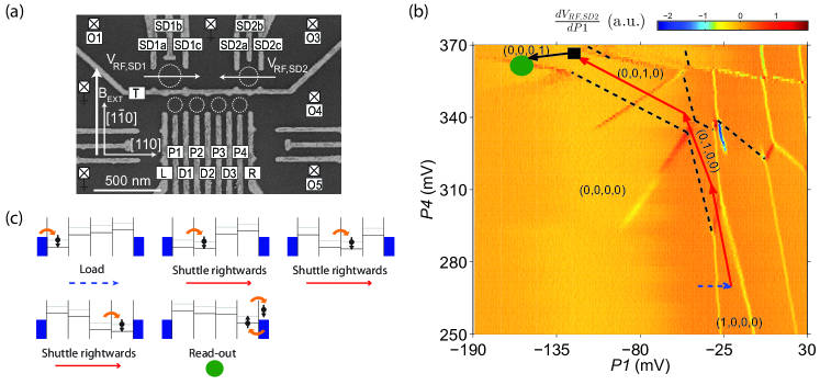
The spin shuttle was initialized by loading a random electron-spin from the left reservoir into dot 1, as described by the schematic diagrams of Fig. 1(c) and implemented by the pulse sequence depicted by the arrows in Fig. 1(b). The loading of a random electron typically results in a spin mixture of 35% spin- and 65% spin- Elzerman et al. (2004). Next, we quickly change the electrochemical potential of dot 1 and 2 in such a way that the electron will shuttle to dot 2. This is repeated for dot 2 to 3, and finally for dot 3 to 4 following the red arrows of Fig. 1(b). The electrochemical potential of dot 4 is then tuned to the position of the green circle in Fig. 1(b). At this position an excited spin- was allowed to tunnel to the reservoir, while a ground-state spin- would remain in the dot. The nearby sensing dot (SD2) was then used to record whether or not the electron had tunneled out, thereby revealing its spin state Elzerman et al. (2004).
The operation of the spin shuttle was tested by performing a variety of measurements. The first two consist of introducing an extra variable waiting time inside either dot 1 or dot 4 which induces spin relaxation to the ground state spin-. We will test if this is reflected in the measurement statistics. For the data represented by the blue curve in Fig. 2, we first load a random electron-spin in dot 1 for 10 s. Next we program a rectangular-shaped voltage pulse of 1 ns that induces tunneling to dot 2, then to dot 3 in 1 ns, afterwards to dot 4 in 97 ns resulting in a total shuttle time of 99 ns and add an extra waiting stage in dot 4. Finally the read-out occurs which takes 320 s. To measure the time in dot 4 the total shuttle time is not critical as long as it is much shorter than . The data shows an expected exponential decay in the measured fraction of spin- of the form , where is proportional to the initial loading probability of a spin-, the relaxation time in dot and an offset. We observe ms and (values in brackets indicate 95% confidence interval).
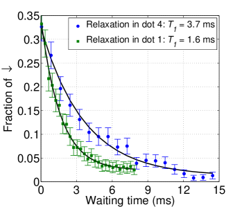
For the data represented by the green curve in Fig. 2 we perform a similar pulse sequence as before, only this time we add the extra waiting stage in dot 1 instead of dot 4. Also, the programmed shuttling time from dot 3 to dot 4 is shortened to 1 ns giving a total shuttling time of 3 ns which is close to the fastest pulse that can be applied by the used pulse generator. We observe ms and . The reported values for are in correspondence with earlier measurements Hanson et al. (2007).
An important ingredient of a spin-shuttle is preservation of the spin state during a shuttle. This state could be influenced whilst shuttling due to a variety of mechanisms: (1) charge exchange with the reservoirs, (2) spin-orbit (SO) interaction and (3) hyperfine interaction with the nuclear spins of the quantum-dot host material. A detailed discussion is given in Ref. 14. To determine if spin flips occur, we can compare the value of and . For the measurement in dot 4, corresponds to ‘1 minus the spin- read-out fidelity’, assuming perfect spin- initialization by thermalization Baart et al. (2016). describes the probability to measure a spin- in dot 4, after having created a spin- in dot 1 by waiting infinitely long. The read-out fidelity does not depend on in which dot the process is induced, or on the shuttling time from dot 1 to 4. As a consequence, the value of can be used to determine if spin flips have occurred as a spin- from dot 1 is shuttled to dot 4. If is larger than , this would indicate spin flips. Since the confidence intervals for and overlap, we conclude that there is no evidence for spin flips during shuttling.
The measurements so far strongly indicate that we have good control over where the electron spin resides (different ’s), and that no spin-flips are induced even when shuttling at high speed throughout the array (similar ’s). However, due to the relatively long read-out time of 320 s it was still possible that even though we programmed a pulse sequence that should correspond to a shuttle time of 3 ns from dot 1 to 4, the electron actually remained for a longer time in one of the dot(s) and only shuttled to dot 4 somewhere during the read-out stage. During such an event, the electron lagging behind would temporarily be in a dot whose electrochemical potential is above the Fermi-level of the reservoirs and has sufficient energy to potentially leave the dot array. If it leaves, a new random electron will enter the array which would be detrimental for the shuttle-functionality. Alternatively, the electron stays within the array and continues the shuttle to end up in dot 4.
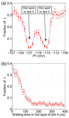
To gain more insight in when the electron actually arrives in dot 4, we added an extra stage to the pulse sequence that corresponds to a so-called ‘hot spot’ in dot 4. At the location of this hot spot, spin-orbit and hyperfine interactions rapidly mix the spin excited state ‘’ with the orbital excited state ‘’. Spin-conserving orbital relaxation quickly transfers the state ‘’ to ‘’. As a result, the ‘’ state will relax on a sub-microsecond timescale to the ground state ‘’ Srinivasa et al. (2013). We will now use a similar pulse sequence as before, only with the inclusion of the hot spot inside dot 4. If the electron spin indeed follows the prescribed pulse sequence, it will hit the hot spot and relax. If the electron however resides for some more time in dot , it will afterwards miss the hot spot and will still show a significant spin- fraction. To identify the location of the hot spots we again load a random electron-spin in dot 1, pulse to dot 2 in 1 ns, then to dot 3 in 1 ns and next to a varying location along the inter-dot transition of dot 3 and 4 for 500 ns; the result is shown in Fig. 3(a). This clearly shows two prominent locations where the spin has completely relaxed. The dip at mV corresponds to the hot spot in dot 4, and is depicted by a black rectangle in Fig. 1(b). The other dip ( mV) corresponds to the hot spot in dot 3 and is not used in this experiment.
To get an upper bound for the shuttling speed we apply a sequence where we again hop from dot 1 to 2, and dot 2 to 3 in 1 ns each, and then pulse to the hot spot in dot 4 for a varying amount of time; the result is shown in Fig. 3(b). This shows that after waiting 150 ns, the whole spin state has relaxed resulting in an upper bound of shuttling of 150 ns. For quantifying this upper bound we are now limited by the relaxation time of the hot spot in dot 4. We have verified that by using just dot 4 (i.e. load in dot 4, move to hot spot, and read-out from dot 4) that 150 ns is the fastest relaxation time of this hot spot.
The upper bound of 150 ns is not yet enough to guarantee that a coherent spin transfer can be performed inside a GaAs device with a ns. It is however promising that the spin shuttle seems to function without loss of spin-information for a pulse time as short as 3 ns such as shown in Fig. 2, indicating that a coherent transfer could already be feasible in this system. This is in agreement with the observation that all inter-dot tunnel couplings exceed 2.5 GHz. In practice, the tunneling may be happening on the timescale of the rise time of the pulse, such that the tunnel events could be adiabatic with respect to the inter-dot anticrossings. In each case, 150 ns is fast enough in different host materials such as Si or Si/SiGe where this shuttling technique could in principle also be applied and the dephasing time has been measured to be much longer 120 s Veldhorst et al. (2014). It still has to be shown that such structures can reach high tunnel couplings, although first steps have recently been made in a triple-quantum-dot device Eng et al. (2015).
In summary, we have demonstrated a spin shuttle inside a quadruple-quantum-dot device where an electron-spin is shuttled within at most 150 ns across the four dots. This work forms the next step in performing a spin shuttle using electrostatic gates that demonstrates preservation of a quantum superposition, an essential ingredient for powerful quantum computing architectures.
Acknowledgements.
The authors acknowledge useful discussions with the members of the Delft spin qubit team, and experimental assistance from M. Ammerlaan, J. Haanstra, R. Roeleveld, R. Schouten, M. Tiggelman and R. Vermeulen. This work is supported by the Netherlands Organization of Scientific Research (NWO) Graduate Program, the Intelligence Advanced Research Projects Activity (IARPA) Multi-Qubit Coherent Operations (MQCO) Program and the Swiss National Science Foundation.References
- Hanson et al. (2007) R. Hanson, L. P. Kouwenhoven, J. R. Petta, S. Tarucha, and L. M. K. Vandersypen, Reviews of Modern Physics 79, 1217 (2007).
- Zwanenburg et al. (2013) F. A. Zwanenburg, A. S. Dzurak, A. Morello, M. Y. Simmons, L. C. L. Hollenberg, G. Klimeck, S. Rogge, S. N. Coppersmith, and M. A. Eriksson, Reviews of Modern Physics 85, 961 (2013).
- Kloeffel and Loss (2013) C. Kloeffel and D. Loss, Annual Review of Condensed Matter Physics 4, 51 (2013).
- Petta et al. (2005) J. R. Petta, A. C. Johnson, J. M. Taylor, E. A. Laird, A. Yacoby, M. D. Lukin, C. M. Marcus, M. P. Hanson, and A. C. Gossard, Science 309, 2180 (2005).
- Nowack et al. (2007) K. C. Nowack, F. H. Koppens, Y. V. Nazarov, and L. M. K. Vandersypen, Science 318, 1430 (2007).
- Medford et al. (2013) J. Medford, J. Beil, J. M. Taylor, S. D. Bartlett, A. C. Doherty, E. I. Rashba, D. P. Divincenzo, H. Lu, A. C. Gossard, and C. M. Marcus, Nature Nanotechnology 8, 654 (2013).
- Kawakami et al. (2014) E. Kawakami, P. Scarlino, D. R. Ward, F. R. Braakman, D. E. Savage, M. G. Lagally, M. Friesen, S. N. Coppersmith, M. A. Eriksson, and L. M. K. Vandersypen, Nature Nanotechnology 9, 666 (2014).
- Veldhorst et al. (2014) M. Veldhorst, J. C. C. Hwang, C. H. Yang, A. W. Leenstra, B. de Ronde, J. P. Dehollain, J. T. Muhonen, F. E. Hudson, K. M. Itoh, A. Morello, and A. S. Dzurak, Nature Nanotechnology 9, 981 (2014).
- Thalineau et al. (2012) R. Thalineau, S. Hermelin, A. D. Wieck, C. Bäuerle, L. Saminadayar, and T. Meunier, Applied Physics Letters 101, 103102 (2012).
- Takakura et al. (2014) T. Takakura, A. Noiri, T. Obata, T. Otsuka, J. Yoneda, K. Yoshida, and S. Tarucha, Applied Physics Letters 104, 113109 (2014).
- Taylor et al. (2005) J. M. Taylor, H. A. Engel, W. Dur, A. Yacoby, C. M. Marcus, P. Zoller, and M. D. Lukin, Nature Physics 1, 177 (2005).
- Kielpinski et al. (2002) D. Kielpinski, C. Monroe, and D. J. Wineland, Nature 417, 709 (2002).
- Bertrand et al. (2015) B. Bertrand, S. Hermelin, S. Takada, M. Yamamoto, S. Tarucha, A. Ludwig, A. D. Wieck, C. Bäuerle, and T. Meunier, (2015), arXiv:1508.04307 .
- Baart et al. (2016) T. A. Baart, M. Shafiei, T. Fujita, C. Reichl, W. Wegscheider, and L. M. K. Vandersypen, Nature Nanotechnology 11, 330 (2016).
- Elzerman et al. (2004) J. M. Elzerman, R. Hanson, L. H. Willems Van Beveren, B. Witkamp, L. M. K. Vandersypen, and L. P. Kouwenhoven, Nature 430, 431 (2004).
- Barthel et al. (2010) C. Barthel, M. Kjærgaard, J. Medford, M. Stopa, C. M. Marcus, M. P. Hanson, and A. C. Gossard, Physical Review B 81, 161308 (2010).
- Yang et al. (2014) C. H. Yang, A. Rossi, N. S. Lai, R. Leon, W. H. Lim, and A. S. Dzurak, Applied Physics Letters 105, 183505 (2014).
- Srinivasa et al. (2013) V. Srinivasa, K. C. Nowack, M. Shafiei, L. M. K. Vandersypen, and J. M. Taylor, Physical Review Letters 110, 196803 (2013).
- Eng et al. (2015) K. Eng, T. D. Ladd, A. Smith, M. G. Borselli, A. A. Kiselev, B. H. Fong, K. S. Holabird, T. M. Hazard, B. Huang, P. W. Deelman, I. Milosavljevic, A. E. Schmitz, R. S. Ross, M. F. Gyure, and A. T. Hunter, Science Advances 1, e1500214 (2015).
- Long et al. (2006) A. R. Long, M. Pioro-Ladrière, J. H. Davies, A. S. Sachrajda, L. Gaudreau, P. Zawadzki, J. Lapointe, J. Gupta, Z. Wasilewski, and S. A. Studenikin, Physica E: Low-Dimensional Systems and Nanostructures 34, 553 (2006).
- Oosterkamp et al. (1998) T. H. Oosterkamp, T. Fujisawa, W. G. van der Wiel, K. Ishibashi, R. V. Hijman, S. Tarucha, and L. P. Kouwenhoven, Nature 395, 873 (1998).
Supplementary Material
I Methods and materials
The experiment was performed on a heterostructure grown by molecular-beam epitaxy, with a 90-nm-deep 2DEG with an electron density of and mobility of (measured at 1.3 K). The metallic (Ti-Au) surface gates were fabricated using electron-beam lithography. The device was cooled inside an Oxford Triton 400 dilution refrigerator to a base temperature of 22 mK. To reduce charge noise the sample was cooled while applying a positive voltage on all gates (ranging between 100 and 400 mV) Long et al. (2006). Gates , and were connected to homebuilt bias-tees (=470 ms), enabling application of d.c. voltage bias as well as high-frequency voltage excitation to these gates. Frequency multiplexing combined with RF reflectometry of the SDs was performed using LC circuits matching a carrier wave of frequency 81.0 MHz for SD2. The inductors are formed by microfabricated NbTiN superconducting spiral inductors with an inductance of 4.6 H for SD2. The power of the carrier wave arriving at the sample was estimated to be -103 dBm. The carrier signal was only unblanked during readout. The reflected signal was amplified using a cryogenic Weinreb CITLF2 amplifier and subsequently demodulated using homebuilt electronics. Real-time data acquisition was performed using a field-programmable gate array (FPGA DE0-Nano Terasic) programmed to detect tunnel events using a Schmitt trigger. Voltage pulses to the gates were applied using a Tektronix AWG5014. Microwaves were generated using a Rohde & Schwarz SMR40 generator connected to via a homemade bias-tee at room temperature.
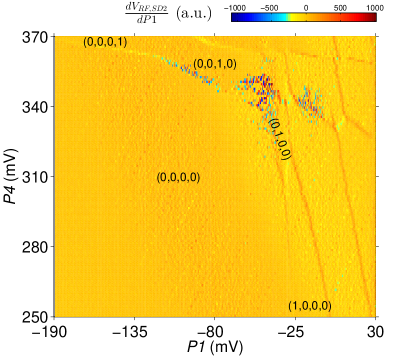
II Charge stability diagram measured on a slow timescale
The charge stability diagram shown in Fig. 1(b) of the main text has been taken in a so-called ‘fast-honeycomb’ mode Baart et al. (2016). Using the bias-tees connected to , and it is possible to step one of them ‘slowly’ using a DAC and apply a triangular ramp on the other using the AWG. This significantly speeds up the measurements compared to stepping both gates using DACs. In Fig. 1(b) of the main text we plot the reverse sweep, i.e. the voltage on the -axis is swept from positive to negative (with a rate of 220 mV/ 4.4 ms). The fading of the charging lines of dot 2 and 3 can then be explained from the indirect coupling with a reservoir Yang et al. (2014). To verify that this is correct, we have also measured Fig. 1(b) in a slow mode where we step both gates using a DAC, the result is shown in Fig. 4.
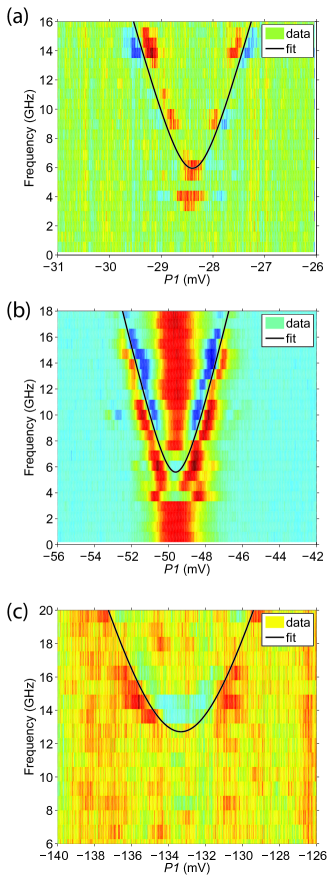
III Measurements of the inter-dot tunnel couplings
The tunnel coupling at zero detuning between neighbouring dots was measured using photon-assisted tunneling (PAT) Oosterkamp et al. (1998), see Fig. 5. The data is fitted to where is the lever arm that is different for each inter-dot transition (not used in this experiment).