Andreev reflection near the Dirac point at Graphene - NbSe2 junction
Abstract
Despite extensive search for about a decade, specular Andreev reflection is only recently realized in bilayer graphene-superconductor interface. However, the evolution from the typical retro type Andreev reflection to the unique specular Andreev reflection in single layer graphene has not yet been observed. We investigate this transition by measuring the differential conductance at the van der Walls interface of single layer graphene and superconductor. We find that the normalized conductance (G/GT>Tc) becomes suppressed as we pass through the Dirac cone via tuning the Fermi level and bias energy, which manifests the transition from retro to non-retro type Andreev reflection. The suppression indicates the blockage of Andreev reflection beyond a critical angle () of the incident electron with respect to the normal between the single layer graphene and the superconductor junction. The results are compared with a theoretical model of the corresponding setup.
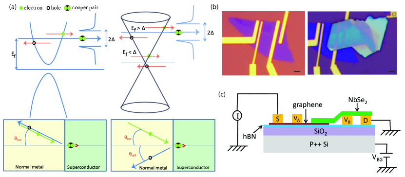
Andreev reflection (AR) Andreev (1964) is the underlying quantum phenomena by which the current flows from a normal (N) region into a superconductor (S) at the normal-superconductor junction. In this process the dissipative current from the normal side converts into dissipation-less super-current in the superconductor. Microscopically an incident electron from the normal side makes a pair with another electron below the Fermi energy () to form Cooper pair at N-S junction. As a result a hole reflects back to the normal side by retracing back the path of the incident electron, which is known as retro Andreev reflection (RAR). However, there can be a physical phenomena in which the conversion of incident electron into the reflected hole is not in the same path, which is known as specular Andreev reflection (SAR) at N-S junction. SAR was not predicated until Beenakker Beenakker (2006, 2008) discovered that this rare phenomena is possible for relativistic electrons in graphene with a superconducting interface. Since then there have been many proposals about SAR in different systems like topological insulator-superconductor junction Majidi and Asgari (2016) and two-dimensional semiconductor with spin-orbit coupling and d-wave superconductor Lv et al. (2012) etc. However, experimentally it remains challenging to observe this effect.
It was pointed out in Ref Beenakker (2006, 2008) that in case of single layer graphene (SLG), when the chemical potential () of the superconductor is far away from the Dirac point ( of SLG >> ) the AR will be retro type, which is an intra-band process as shown in Fig. 1a. There will be a critical value () of the incident electron at the N-S junction beyond which the AR will be blocked. The emerges as a consequence of the conservation of momentum between the incident electron above and reflected hole below . When the of SLG >> the tends to /2, which means the electron can reflects back as a hole with any incident angle from zero to /2. The value of the will decrease as the approaches towards the Dirac point. As a result AR will be progressively suppressed while passing through the Dirac point and AR will be no longer RAR because the path of incident electron and reflected hole will be different. This is the onset of specular type AR. However, when the Dirac point of SLG is within the superconducting gap and < , the will again tend to /2 and as a result AR will be enhanced. In the latter one the AR (Fig. 1a) is inter-band process in which there is a sign change of the hole mass and will be true SAR.
The main difficulties to observe SAR experimentally is the Fermi energy broadening (). For example graphene on substrate has of the order of 100 meV due to charge puddles present on the substrate. Very recently, hexagonal boron nitride () supported bilayer graphene (BLG) has been used to reduce the and the signature of SAR has been observed experimentally Efetov et al. (2015) after a decade of its theoretical prediction Beenakker (2006, 2008). However, for bilayer graphene the energy dispersion is quadratic near the Dirac point as well as there could be band gap opening at charge neutrality point. On the other hand the dispersion in SLG is linear having relativistic massless Dirac fermion characteristics, which gives rise to Klein tunneling at the interface of a p-n junction. Because of this property, even if there is a work function mismatch between the SLG and SLG underneath of superconductor, there will be electron transport through the interface by virtue of AR. Therefore, investigating the transition from RAR to SAR in SLG would help to understand the underlying Andreev process in graphene-superconductor junctions. In this article we have carried out the transport measurements on normal - SLG - superconductor junction, where the SLG has been supported by and achieve 10 meV. As a superconductor, has been used whose superconducting gap 2 2 meV. The conductance ( = ) measurements with the carrier density and bias reveal that the normalized conductance () becomes suppressed as we pass through the Dirac point. The suppression of conductance around the Dirac point matches fairly well with our theoretical calculation based on Blonder-Tinkham-Klapwijk (BTK) formalism Blonder et al. (1982); Beenakker (2008). Our results with the theoretical support unveil the onset of transition from retro AR to non retro type AR in SLG-superconductor interface.
Fig. 1b shows an optical image of a SLG on . A thin layer of hBN ( 10nm) was first exfoliated on a wafer. This was followed by transfer of SLG on by dry transfer technique Dean et al. (2010). The contacts for SLG and predefined contacts for were made of Cr/Au(5/70 nm) using standard electron beam lithography. At the last step a thin ( 20nm) was transferred on SLG and predefined contacts, as shown in Fig. 1b. We should mention that in order to avoid the oxidization of the bottom surface of , the was transferred within few minutes after fresh exfoliation of a bulk flake. The schematic of the measurement is shown in Fig. 1c, where the conductance between the normal(Au) - SLG - superconductor () has been measured using conventional lock-in technique. All the measurements were carried out in a refrigerator having base temperature of 236mK. The typical contact resistances between Au-graphene and Au- are less than a hundred of Ohm where as the graphene - interfaces show 1.5-3.0 kOhm contact resistance (details in supplementary information - Fig. S1). In this article, we have repeated the experiments for two more representative devices. In the S.I.(Fig. S2), we have also shown the characterization of thin flake transferred on predefined gold contacts and found the 2meV, which also match very well with the critical temperature (Tc 6.5K) measurement.
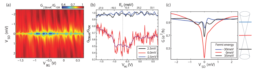
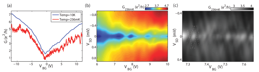
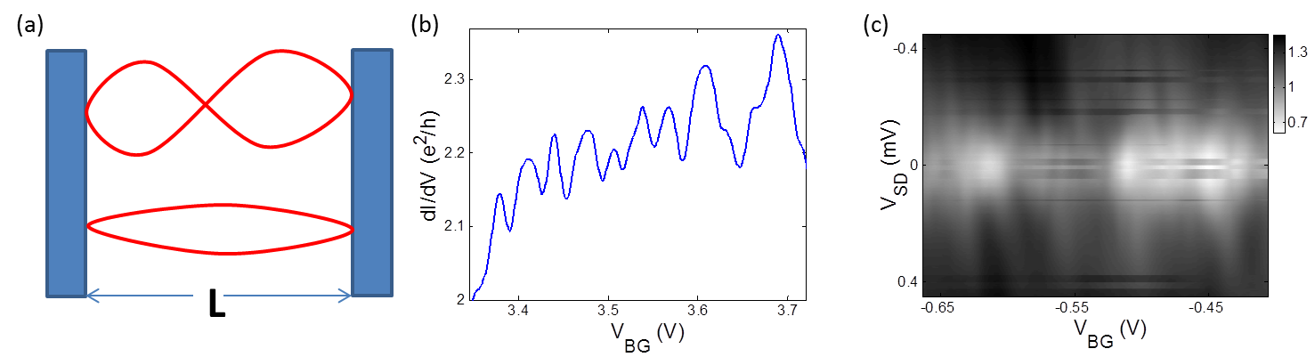
Fig. 2a shows the of one of our representative devices as a function of gate voltage () at 10K and 236mK. The conductance almost increases linearly with . By analyzing the 10K data we extract the mobility (), in-homogeneity () and of the device, which are 12,000 cm2V-1s-1, 1010cm-2 and 10meV, respectively (for details Fig. S3). The most distinct differences at two temperatures are the fine oscillations at 236mK. In order to understand the origin of these quasi periodic oscillations we have carried out the as a function of and (bias), shown as 2D colormaps in Fig. 2b and Fig. 2c. Fig. 2c clearly shows diamond type of oscillation, which are signature of Fabry-Perot (F.P.) oscillations and reported in graphene Josephson junctions by many groups Rocha et al. (2010); Allen et al. (2015); Shalom et al. (2015); Calado et al. (2015). The F.P oscillation is due to the formation of standing waves between the normal - SLG and SLG - superconductor interface, which fairly match with our device dimension (for details Fig. S4). The above results show the ballistic nature of our normal-SLG-superconductor device at low temperature.
It can be seen from Fig. 2b and 2c that at 236mK the has always lower value at = 0 compared to finite irrespective of . For T > Tc, is almost independent of (S.I.). With lowering the temperature, the dip at = 0 starts appearing below Tc (S.I.-Fig. S3). At 236mK the superconducting gap at 1meV with the subgap features at 0.3meV are observed (S.I.). As discussed before the subgap features are due to F.P. oscillations. Within the superconducting gap the electron can transport by Andreev reflection. For a transparent (barrier strength, Z=0) SLG-superconductor interface the conductance should double because of equal contribution coming from the reflected hole, which adds up as excess current. However, for an interface with Z > 0.5 there will be a decrease in conductance within the superconducting gap. Our data suggests Z 0.7, which corresponds to a transparency, T 0.7 (T = 1/1+Z2) at SLG-superconductor interface Blonder et al. (1982) (S.I for details). In order to see the crossover from RAR to SAR around the Dirac point we plot the normalized 2D colomap () in Fig. 3a. It can be clearly seen that above superconducting gap the normalized conductance is independent of but close to zero bias ( 0.3mV) the normalized conductance is suppressed around the Dirac point. This is clearly visible in Fig. 3b, where the normalized conductance is plotted as a function of for = 0 and = 2.5mV. The similar suppression can be also seen if we take the vertical cuts from Fig. 3a at different as shown in Fig. 3c, where the at = 0 is minimum close to the Dirac point.
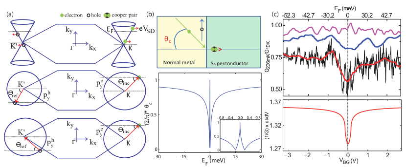
For AR at SLG-superconductor interface, an incident electron above the Fermi energy () makes a Cooper pair with an electron below the Fermi energy () having opposite spin and opposite valley Beenakker (2006), as shown in Fig. 4a (top). The missing electron below returns as hole and thus the current flow at the interface. The component of momentum () along the interface must be strictly conserved and the component of hole velocity perpendicular to the interface must be negative to that of incident electron. These two conditions will restrict the hole to be at a specific point in - plane, as shown in fig 4(a) (middle). As the radius of constant energy contour decreases with decreasing Fermi energy, the angle of reflected hole () will be larger than the angle of incident electron (). Therefore, beyond a critical angle () of incident electron the will exceed 90 degree and thus AR process will stop (Fig. 4b - top). The can be expressed as following Beenakker (2006, 2008); Bhattacharjee and Sengupta (2006).
| (1) |
Using Eqn.1 the (normalized by total angle /2) as a function of is shown in Fig. 4b for = 0.2mV. It can be seen that far away from the Dirac point the is close to /2, which means the incident electron can reflect back as a hole with any incident angles ( from zero to /2). With lowering the the decreases. However, when the is close to the Dirac point the AR is specular type (Fig. 4a - bottom) and in that case again becomes /2. In order to compare with the experimental data one needs to calculate the differential conductance. For that we need to know the coefficient of andreev reflection() as well as normal reflection(). These probabilities depend on the position of Fermi energy as well as on angle of incident electron ( = ). The differential conductance has been numerically calculated using the following expression based on BTK formula Blonder et al. (1982); Beenakker (2006).
| (2) |
is the ballistic conductance of graphene channel, where is the number of transverse modes present in the graphene channel. The expression of and are given in the S.I. Beenakker (2006). Using those expressions and Eqn. 2 we have calculated x as a function of VBG for different Fermi energy broadening, as shown in Fig. S5. To compare our experimental data (red line Fig. 4c-top) we show the theoretical calculation for 12 meV in Fig. 4c - bottom. It can be seen from Fig. 4c that the experimental data qualitatively agrees with the theory. The discrepancy between the experimental and theoretical values could be due the finite barrier (Z 0.7) at SLG-superconductor interface, which was not considered in theory.
Now we will consider the possible effect due to the finite contact resistance (1.5-3.0 kOhm) at the SLG-superconductor interface. It is known that for graphene the contact resistance changes with . However, with shift, if the contact resistance below and above Tc changes in a similar manner (in percentage), it will not contribute to the normalized conductance (). This is justified in Fig. 3b for higher bias data. Even if there are changes in contact resistance (below and above Tc) with shifting , it will be a gradual effect contrary to our observation in Fig. 3b for the zero bias data. We have also seen that the suppression is much weaker for SLG-NbSe2 device having higher 30meV (blue line in Fig. 4c-top).
In conclusion we have carried out the quantum transport measurement at SLG-NbSe2 junction. Our device showing Fabry-Perot type oscillations at low-temperatures indicates the ballistic nature of our normal - SLG - superconductor device. The normalized conductance (G236mK/G10K) above the superconducting gap (VSD > ) does not depend on the position of Fermi energy. On the other hand inside the superconducting gap the normalized conductance gets suppressed as we pass through the Dirac point. The suppression is understood in terms of blockage of AR beyond a critical angle at SLG - superconductor interface, which is also indication of non retro type AR because the paths for incident electrons and reflected holes are different, which is indeed the onset for SAR. However, we do not observe the signature of true specular AR at the Dirac point due to > . Our experimental data matches fairly well with our theoretical calculation based on BTK formula, which will help to understand the future experiments related to this field.
Authors thank Vivas Bagwe for preparing the NbSe2 single crystals. Authors thank Dr. Abhiram Soori, Dr. Bhaskar Kaviraj and Dr. Tanmoy Das for stimulating discussions. AD also thanks nanomission under Department of Science and Technology, Government of India for financial support.
SUPPLEMENTARY INFORMATION
I Determination of contact resistance at SLG-NbSe2 junction
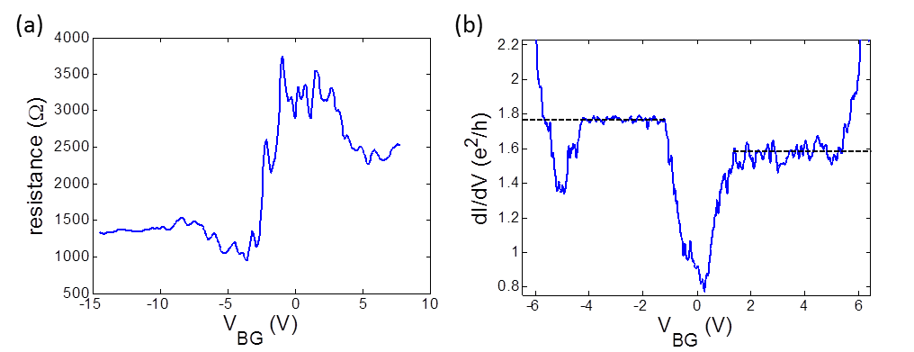
By measuring the resistances of our device in four probe and three probe configuration we extract out the contact resistances between SLG-gold contact and NbSe2-gold contact, which are 100 and 70, respectively. In order to know the contact resistance between the SLG and NbSe2 we have used the following method. We first extract out the resistivity of SLG alone from the R Vs VBG plot and then extrapolate for the SLG channel part between gold and NbSe2. At the end the contact resistance at the SLG-NbSe2 junction is determined by subtracting the SLG channel resistance from four probe gold-SLG-NbSe2 resistance, which has been shown in Fig. 1a as a function of gate voltage. It can be seen that for hole and electron sides the junction resistances are and , respectively. These values can be further justified by looking at the values of quantum Hall plateaus in SLG. Fig. 4b shows the quantum hall plateau of SLG at B = 4 Tesla. From the deviation of quantum conductance values we have evaluated the values of contact resistances. Contact resistance in the hole side is order of and in the electron side order of , which matches fairly well with the Fig. 1a.
II Characterization of NbSe2
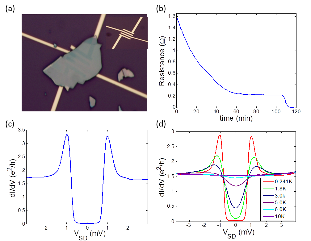
Few layer NbSe2 is characterized to see the superconducting transition and to get the value of superconducting gap. One of such device is shown in Fig 2a, first predefined contacts are made and NbSe2 flake is transferred at the last stage. Usually the transfer has to be done quickly, we observed that the time taken to transfer from the time of exfoliation decides the quality of contact in the devices. Our best devices in which transfer is done within 5 minutes shows contact resistance of 100 ohm. The four probe resistance in the device shown in Fig 2a is found to be 2.5 ohm at room temperature. We found the transition temperature around 7K, in fig 2b the resistance is plotted with time while inserting the dipstick inside the He4 Dewar. In another device we allowed the NbSe2 to oxidize to form an insulating layer. In this device we did the differential conductance and found the BCS peaks at 1mV as shown in fig 2c. We observed the evolution of these peaks with temperature and found that it is vanishing above 6K.
III Charge in-homogeneity and Fermi energy broadening in the sample
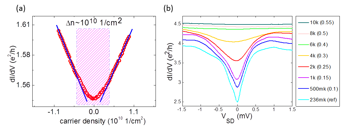
To see many interesting properties of graphene it has to be suspended or supported over hBN Dean et al. (2010). This is because when graphene is directly exfoliated on Si/SiO2 substrate it becomes unevenly doped all over because of charge puddles present on the wafer which is mainly because of dangling bonds present on surface of amorphous SiO2 as well as trap charges in oxides. hBN being an inert crystal improves the quality of graphene channel when supported over hBN. Fig. 3a shows the evaluation of charge in-homogeneity of the device presented in the manuscript. We have achieved n0=1010 cm-2 which corresponds to Fermi energy broadening of 10 meV.
IV Fabry Perot oscillations
Due to presence of barriers at both sides of the graphene channel, it works as a Fabry Perot cavity for electrons giving rise to quasi peridic oscillations in conductance. For a specific gate voltage , carrier density where is the capacitance per unit area. Fermi wave vector where is the Fermi wavelength. Condition for constructive interference is , where m is the integer and d is the channel length. This will determine the peaks in conductance plot. By knowing the position of any two peaks we can evaluate the approximate length scale the oscillations corresponds to. The major oscillations appear with periodicity of in Fig. 2b of the manuscript. corresponds to a length of 0.65 , which is close to the channel length (1.0 ). The discrepancy has been reported earlier Allen et al. (2015) and attributed to the formation of p-n junction at the interfaces as well as electric field screening, which reduces the effective length scale.
V Analysis of the Transmission probability at SLG-NBSe2 junction
The NS junction is modeled using BTK theory and the transmission probability is evaluated Blonder et al. (1982). In our previously made graphene devices we found the contact resistance between gold and graphene to be hundred ohms. In this device the resistance of graphene NbSe2 junction must be few kilo ohms, so we are neglecting the effect of barrier between gold and graphene. According to BKT theory normal and superconducting state transmission probabilities are given by 1/1+Z2 and 1/ respectively. From the ratio of superconducting state conductance and normal state conductance we evaluate the value of Z=0.73. Finally we got the transmission probability to be 0.7.
VI Calculation of differential conductivity
The differential conductance through a graphene-superconductor junction can be calculated only after knowing the probabilities of Andreev reflection and normal reflection. We need to solve the Bogoliubov-De Gennes equations in both sides of the junction with appropriate boundary conditions to get the expressions of these probabilities Beenakker (2006, 2008). The probabilities depends on the angle of incidence and the Fermi energy both. Calculation will also give a critical angle beyond which andreev reflection is not allowed as we have explained in the main text by direct observation of the electron hole conversion process. The amplitudes of Andreev reflection() and normal reflection() can be writtten Beenakker (2006) in terms of angle of incidence(), angle of reflection(), critical angle() and the superconducting phase() as
| (3) |
where,
| (4) |
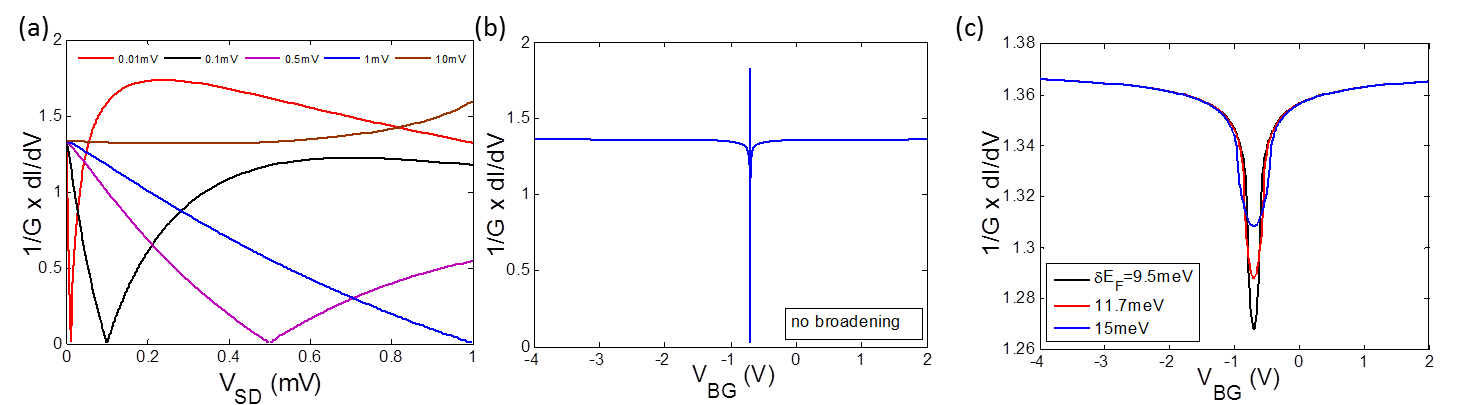
In fig 4(a) x is plotted as a function of excitation energy for different equilibrium Fermi energies. It shows different spectrum for low and high Fermi energy. In fig 4(b) x is plotted as a function of . To compare our experimental result we introduced a finite Gaussian broadening in the system. We assumed the net conductance is effectively the average of ideal channels each with a uniform doping, the doping amount is equivalent to presence of an extra gate voltage .
| (5) |
Where is the broadening and is the experimental Dirac point position (voltage where conductance is minimum). In fig 4(c) x is plotted for different broadening. It can be noted that normalized value is more than one. However, with Z in the calculation of x the normalized differential conductance value will drop down below one. As the effect of barrier is not considered in the calculation of differential conductance, the superconducting state conductance exceeds normal state conductance due to excess current.
References
- Andreev (1964) A. Andreev, Sov. Phys. JETP 19, 1228 (1964).
- Beenakker (2006) C. W. J. Beenakker, Phys. Rev. Lett. 97, 067007 (2006).
- Beenakker (2008) C. Beenakker, Rev. Mod. Phys. 80, 1337 (2008).
- Majidi and Asgari (2016) L. Majidi and R. Asgari, Phys. Rev. B 93, 195404 (2016).
- Lv et al. (2012) B. Lv, C. Zhang, and Z. Ma, Phys. Rev. Lett. 108, 077002 (2012).
- Efetov et al. (2015) D. Efetov, L. Wang, C. Handschin, K. Efetov, J. Shuang, R. Cava, T. Taniguchi, K. Watanabe, J. Hone, C. Dean, et al., Nature Phys. (2015).
- Blonder et al. (1982) G. Blonder, M. Tinkham, and T. Klapwijk, Phys. Rev. B 25, 4515 (1982).
- Dean et al. (2010) C. R. Dean, A. F. Young, I. Meric, C. Lee, L. Wang, S. Sorgenfrei, K. Watanabe, T. Taniguchi, P. Kim, K. Shepard, et al., Nature nanotechnology 5, 722 (2010).
- Rocha et al. (2010) C. G. Rocha, L. E. F. Torres, and G. Cuniberti, Phys. Rev. B 81, 115435 (2010).
- Allen et al. (2015) M. Allen, O. Shtanko, I. Fulga, J.-J. Wang, D. Nurgaliev, K. Watanabe, T. Taniguchi, A. Akhmerov, P. Jarillo-Herrero, L. Levitov, et al., arXiv preprint arXiv:1506.06734 (2015).
- Shalom et al. (2015) M. B. Shalom, M. Zhu, V. Fal’ko, A. Mishchenko, A. Kretenin, K. Novoselov, C. Woods, K. Watanable, T. Taniguchi, A. Geim, et al., Nature Physics (2015).
- Calado et al. (2015) V. Calado, S. Goswami, G. Nanda, M. Diez, A. Akhmerov, K. Watanabe, T. Taniguchi, T. Klapwijk, and V. L, Nature Nanotechnology 10, 761 (2015).
- Bhattacharjee and Sengupta (2006) S. Bhattacharjee and K. Sengupta, Phys. rev. lett. 97, 217001_1 (2006).