]http://research.uni-leipzig.de/hlp/
Fundamental absorption edges in heteroepitaxial YBiO3 thin films
Abstract
The dielectric function of heteroepitaxial YBiO3 grown on -Al2O3 single crystals via pulsed laser deposition is determined in the spectral range from 0.03 eV to 4.5 eV by simultaneous modeling of spectroscopic ellipsometry and optical transmission data of YBiO3 films of different thickness. The (111)-oriented YBiO3 films are nominally unstrained and crystallize in a defective fluorite-type structure with space group. From the calculated absorption spectrum, a direct electronic bandgap energy of 3.6(1) eV and the signature of an indirect electronic transition around 0.5 eV are obtained. These values provide necessary experimental feedback to previous conflicting electronic band structure calculations predicting either a topologically trivial or non-trivial insulating ground state in YBiO3.
pacs:
68.55.-a, 71.20.-bI Introduction
During the past ten years, heteroepitaxial YBiO3 thin films were investigated mainly as a buffer layer for epitaxial YBa2Cu3O7-δ high- superconductors.Li et al. (2007); Zhao et al. (2007); Pollefeyt et al. (2013); Meiqiong et al. (2009) Recently, first-principles electronic band structure calculations proposed YBiO3 as a novel oxide topological insulator:Jin et al. (2013) Based on an assumed, undistorted perovskite structure with space group and lattice constant = 5.428 Å, a topologically insulating phase was predicted due to a band inversion between an -like and a = 1/2 band at the point that is driven by the spin-orbit coupling of the Bi states. YBiO3 then has a topological trivial indirect bandgap of 0.18 eV and a non-trivial direct bandgap of 0.33 eV at the point. The size of the direct bandgap and high bulk resistivity were expected to allow for surface-dominated transport at room-temperature. However, a subsequent theoretical study showed that the assumed crystal structure is unstable.Trimarchi et al. (2014) Instead, a distorted perovskite structure is predicted to be most stable and YBiO3 is predicted as a topologically trivial band insulator with larger direct and indirect electronic bandgaps.
Experimentally, solid solutions of YxBi1-xO1.5 with are stable at room-temperature and crystallize in a face-centered cubic, defective fluorite-type structure with space group .Battle et al. (1983, 1986); Kale, Jadhav, and Bichile (1999); Zhang et al. (2010) However, there exist no band structure calculations for the space group. At = 0.5, YxBi1-xO1.5 (YBiO3) has a cubic lattice constant = 5.4188 Å,Zhang et al. (2010) and its pseudo-cubic primitive cell with is closely matched to LaAlO3, SrTiO3, (LaAlO3)(Sr2TaAlO6) (LSAT) and also YBa2Cu3O7-δ. Heteroepitaxial YBiO3(100) thin films have hence been prepared as buffer layers on LaAlO3(001), SrTiO3(001) and LSAT(001) single-crystalline substrates by chemical solutionLi et al. (2007); Zhao et al. (2007); Pollefeyt et al. (2013) and pulsed laser deposition.Meiqiong et al. (2009); de Putter (2014) Their surface-morphology is characterized by crystalline grains of around 50 nm and root-mean-squared (RMS) surface roughnesses between 2.6 to 1.8 nm at a film thickness of 140 and 40 nm, respectively.Zhao et al. (2007); Pollefeyt et al. (2013) Furthermore, pelletized YBiO3 powders showed a high 0.5 M m bulk resistivity at room-temperature and paramagnetic behaviorZhao et al. (2007).
In order to provide some necessary experimental feedback to the conflicting theoretical band structure calculations,Jin et al. (2013); Trimarchi et al. (2014) we report here an estimate of the direct electronic bandgap of two relaxed-textured YBiO3(111) films deposited using pulsed laser deposition with different thickness on -Al2O3 single crystals. Structural analyses confirm their crystallization in a defective fluorite-type structure with space group. The dielectric function between 0.03 eV and 4.5 eV is determined by simultaneous modeling of spectroscopic ellipsometry and optical transmission data. Contrary to the theoretical band structure calculations, we find evidence for a direct electronic bandgap of 3.6(1) eV and a possible signature of an indirect electronic transition around 0.5 eV in YBiO3.
II Experimental details
The YBiO3 thin films were grown by pulsed laser deposition (PLD) on 10 10 mm2 -plane Al2O3(11-20) single crystals. PLD was performed with a 248 nm KrF excimer laser at a laser fluence of 2 J cm-2. The polycrystalline source target was prepared by conventional solid-state synthesis of Bi2O3 and Y2O3 powders in a 1:1 molar ratio. The starting materials were homogenized, pressed and sintered in air for 24 h at 880 ∘C. After an intermediate regrinding, a second and third sinter step was performed for 12 h in an oxygen atmosphere at 800 ∘C and 1,000 ∘C, respectively.
The deposition process involved a 300 laser pulses nucleation layer grown at a 1 Hz pulse frequency, followed by the deposition of 60,000 and 2,000 pulses at 5 Hz for the thick and thin film, respectively. The films were grown at a growth temperature of approximately 650 ∘C and an oxygen partial pressure of 0.05 mbar to obtain optimal Y:Bi stoichiometry and film crystallinity. After the deposition, the samples were annealed in situ at an oxygen partial pressure of 800 mbar. The film thicknesses were determined as 1660 nm and 57 nm from optical modeling (see text below). Note, that reliable resistivity data was not obtained due to a very large bulk resistance of the 1660 nm film of around 700 M at room-temperature which exceeds our instrument’s measuring range.
X-ray diffraction (XRD) structural analyses were performed with a Panalytical X’Pert PRO Materials Research Diffractometer with parabolic mirror and PIXcel3D detector and Cu Kα radiation. The surface morphology was investigated with a Park Systems XE-150 atomic force microscope (AFM) in dynamic non-contact mode. Topographic images were post-processed with the Gwyddion software.Nečas and Klapetek (2012) The chemical composition was measured by energy-dispersive X-ray spectroscopy (EDX) using an FEI Novalab 200 scanning electron microscope (SEM) equipped with an Ametek EDAX detector. The thin film dielectric function and layer thickness were determined via standard variable angle spectroscopic ellipsometry (VASE, IR-VASE by J.A. Woolam, Inc.) in the spectral range from 0.03 eV to 4.50 eV and UV/VIS transmission spectroscopy (Perkin Elmer Lambda 19) between 0.62 eV and 6.20 eV.
III Results and discussion
III.1 Structural properties
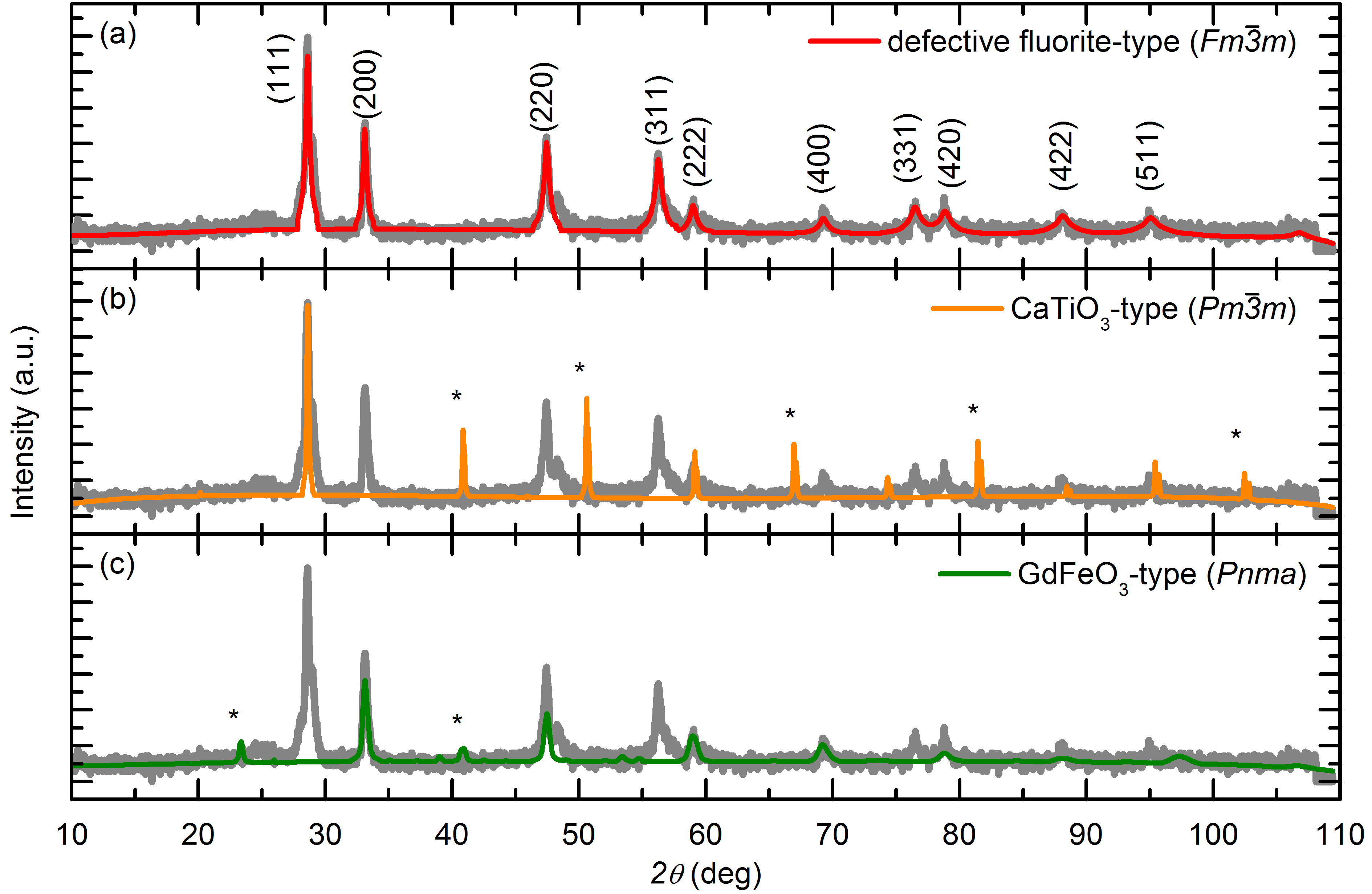
Figure 1 shows an XRD --scan of the polycrystalline YBiO3 source target. The pattern is fit successfully by the Rietveld methodRietveld (1969) using the defective fluorite-type structural model by Zhang et al.Zhang et al. (2010) and a cubic lattice constant = 5.4279(4) Å. There exist minor additional peaks that very likely relate to the unreacted starting materials, and possibly elemental Bi and Bi2O3-x.Pollefeyt et al. (2013) We note, that the assumed and models fail to match with all of the observed YBiO3 reflexes, see Supplementary Material. EDX yields a Y:Bi ratio of 0.98:1 which suggests that good stoichiometric transfer is feasible in spite of the incomplete target phase purity.
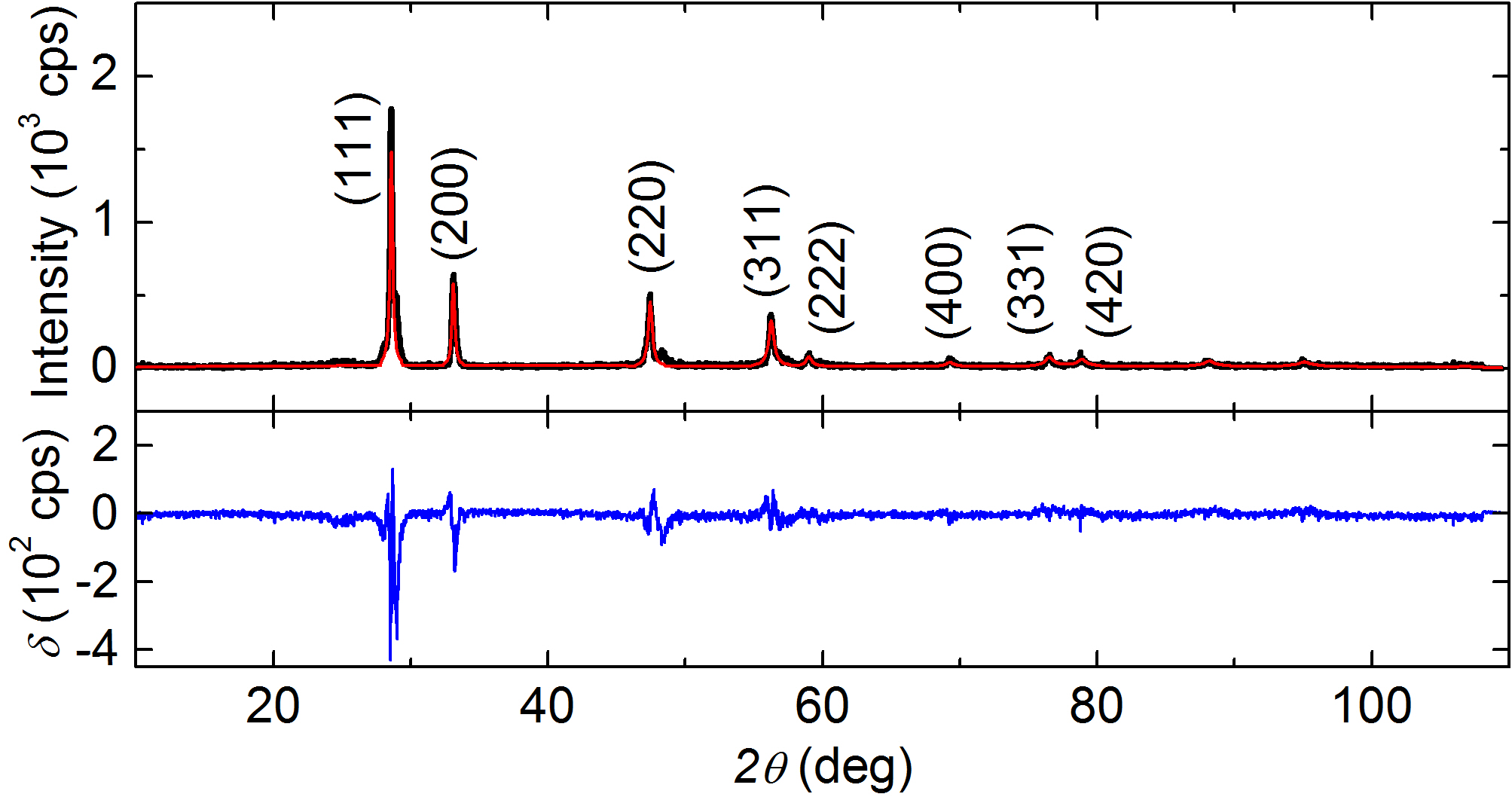
Figure 2(a) shows the - patterns of two YBiO3 films with a thickness of 1660 nm (film A) and 57 nm (film B), respectively, deposited on -Al2O3 single crystals. The patterns are indexed according to the experimental unit cellBattle et al. (1983, 1986); Kale, Jadhav, and Bichile (1999); Zhang et al. (2010) and indicate very good (111) preferential out-of-plane orientation. For film A, the pattern shows additional minor peaks ( cps) related to other allowed YBiO3 reflexes. By extrapolation of the values of the (111), (222) and, if possible, the (333) reflexes to ,Nelson and Riley (1945) very similar out-of-plane lattice constants of 5.3907(2) Å and 5.42(4) Å are determined for films A and B, respectively. These values deviate from the literature value of 5.4188 Å Zhang et al. (2010) and from the Rietveld-refined value of the polycrystalline target by at most 0.5 and 0.7 %, respectively.
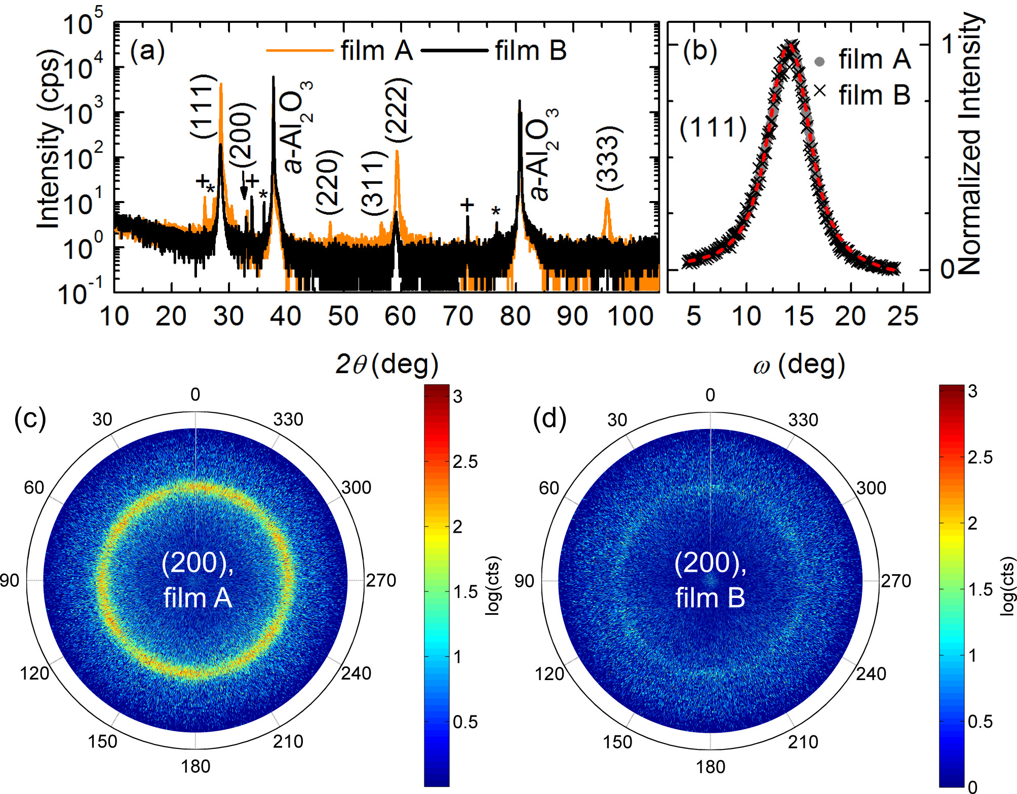
For both films, the XRD -scans (rocking scans) of the YBiO3 (111) reflex, see Fig. 2(b), exhibit identical half-widths of about 5∘ and thus suggest a comparable degree of crystallite mosaicity.
A possible in-plane epitaxial relationship with -Al2O3 was investigated by - pole figures around the asymmetric YBiO3 (200) reflex, see Fig. 2(c,d). For both films A (c) and B (d), a distinct circular intensity maximum is evidence for a random distribution of the in-plane crystallite orientation. The lack of a defined in-plane epitaxial relationship is explained by the large lattice mismatch between YBiO3(111) and -Al2O3 of about 40 %.111Assuming a cubic YBiO3(111) epilayer with Å, the lattice mismatch with the 13.00 5.50 Å2 -plane of Al2O3 will be +42 % and -40 %, respectively.
The XRD data indicate relaxed, i.e., nominally unstrained growth of YBiO3(111) on -Al2O3. Thus, the observed preferential out-of-plane orientation suggests, that the YBiO3 (111) surface has the lowest formation energy. Because EDX analyses on both films yield nearly ideal Y:Bi ratios of 1.02:1, the slight deviations of the out-of-plane lattice constant from the literature Zhang et al. (2010) and the polycrystalline target value are likely caused by internal strain due to, e.g., oxygen vacancies.
III.2 Optical properties
The spectra of the dielectric function were determined from ellipsometry and optical transmission data of the relaxed grown YBiO3 films A and B. The anisotropic transfer matrix model consists of layers for the YBiO3 film and the surface roughness using a Bruggeman effective medium approximation mixing the dielectric functions of YBiO3 and air in a 1:1 ratio.Jellison et al. (1994) The dielectric functions of the films are modeled using a Kramers-Kronig consistent numerical B-spline model.Johs and Hale (2008) We note, that film A was deposited on a double-sided polished substrate to avoid diffusive scattering in the optical transmission spectroscopy. The substrate backside was subsequently roughened mechanically in order to minimize back surface reflections in ellipsometry. The substrate of film B was single-sided polished. Its wavelength-dependent scattering by the backside roughness in the transmission measurement is corrected for by a reference transmission measurement of a bare double-sided polished substrate with same thickness. Finally, the absorption coefficient is calculated from the numerical B-spline dielectric function.
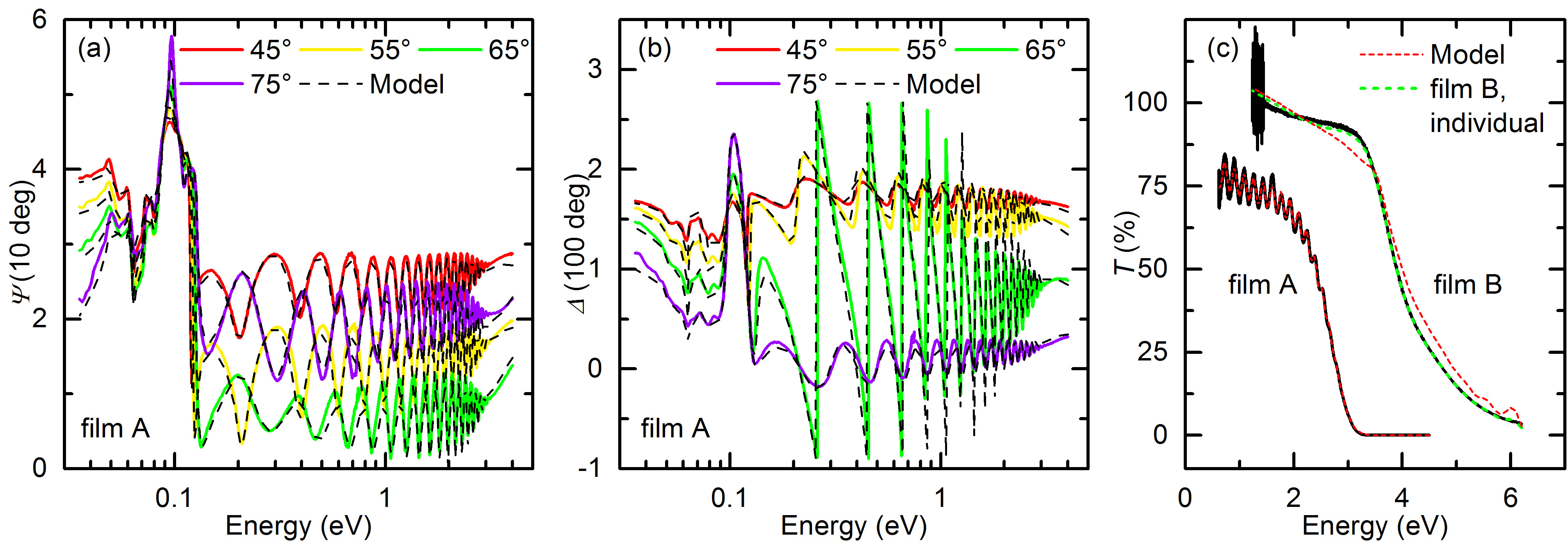
Figure 3(a-c) shows the results of the simultaneous modeling of the reflection ellipsometry (, ) and optical transmission () data of the YBiO3 films A and B. The numerical B-spline model reproduces the experimental data in the entire measured spectral range (a,b). Around 200 meV, substrate backside reflections disturb the ellipsometry spectra. These occur only in this narrow spectral range of large wavelengths where film and substrate are sufficiently transparent. At lower photon energies, the -Al2O3 Restrahlen band prevents this. The modeled data of film B, Fig. 3(c), suffers from a large error as it was measured through a rough backside; in this case, the ellipsometry data is more reliable. The spectra of film A show obvious layer thickness oscillations. For films A and B, thicknesses of = 1660(30) nm and = 57(2) nm are obtained from the fits. The modeled effective surface roughnesses are approximately 25 nm and 3 nm, respectively. These values agree well with surface roughness values obtained via AFM, see Supplementary Material.
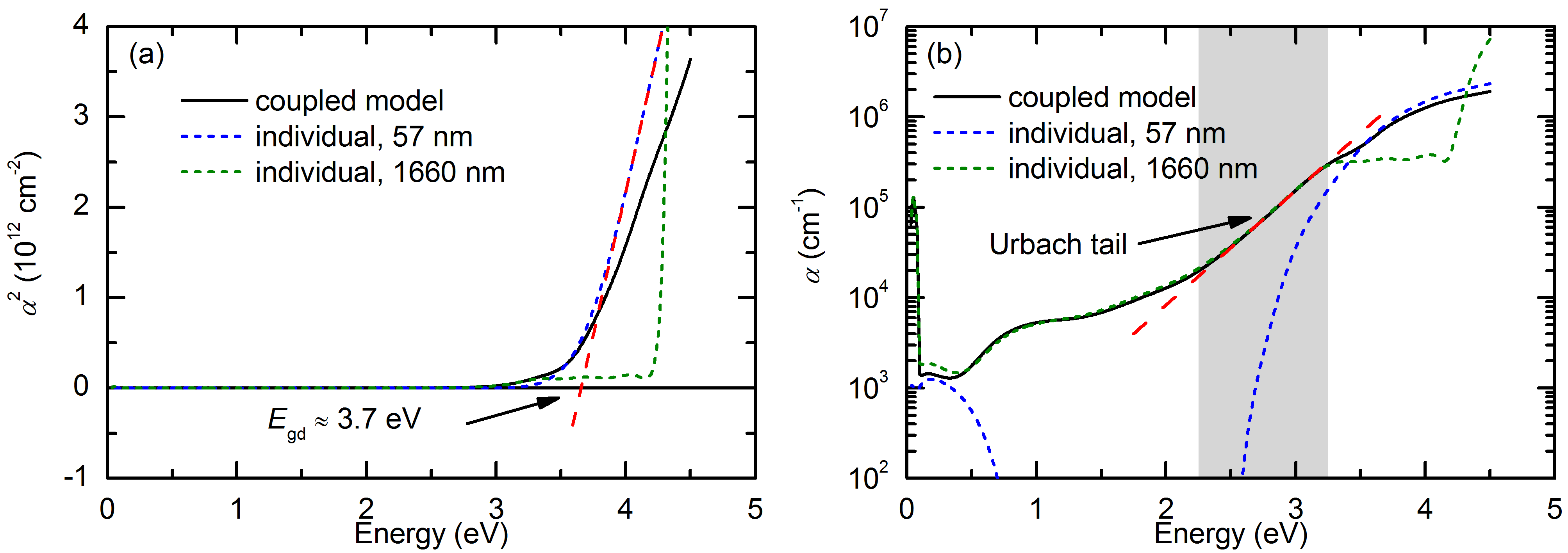
From the numerical model dielectric function the absorption coefficient is calculated and plotted in Fig. 4 as and , respectively. Based on the present data, we can exclude indirect and direct bandgaps at 0.183 eV and 0.33 eV, as predicted by the band structure calculations of Jin et al.Jin et al. (2013) Instead, strong absorption is evident above 3 eV together with a continuous onset at about 0.5 eV. At about 0.05 eV, a phonon resonance is evident. The strong absorption peak is interpreted in analogy to Trimarchi et al. Trimarchi et al. (2014) as the allowed direct bandgap transition between the Bi and bands at the point. For an estimate of the direct bandgap energy , linear regression of the spectrum, Fig. 4(a), between 3.75 eV and 4.50 eV is performed.Fujiwara (2007) The extrapolation of the straight line fit to 0 yields = 3.6(1) eV. Furthermore, we tentatively associate the slight absorption starting at around 0.5 eV, visible in Fig. 4(b), with the allowed indirect bandgap transition from the valence band maximum at the point to the conduction band minimum at the point.Trimarchi et al. (2014) To cross-check the reliability of our model, we have also modeled films A and B individually, as shown in the Supplementary Material: While the model of the thin film B yields the same direct bandgap, cf. Fig. 3(c), but is insensitive to low-energy absorption, modeling the thick film A is required to reveal a possible Urbach tail between 2.25 eV and 3.25 eV.
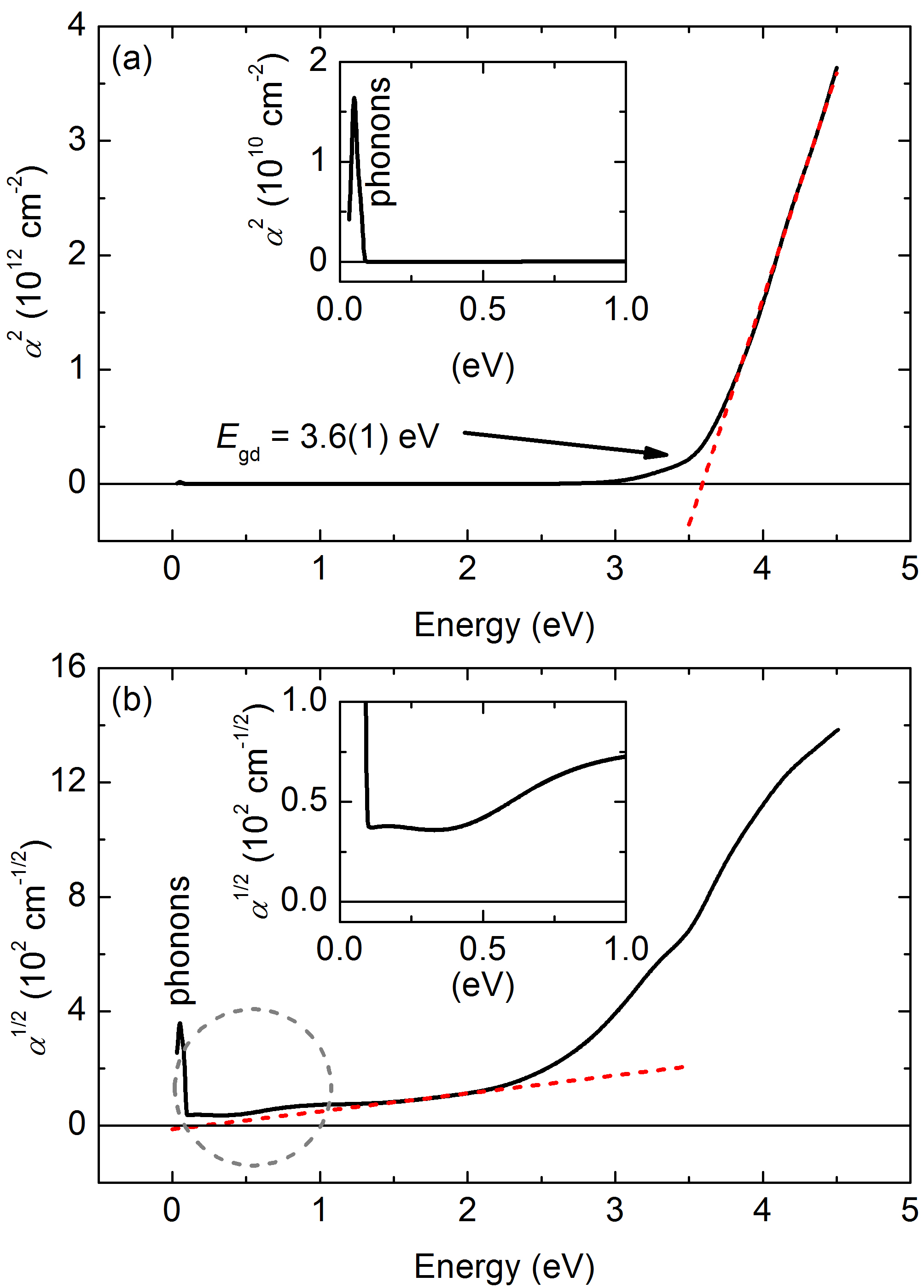
The obvious discrepancy between the predicted Jin et al. (2013); Trimarchi et al. (2014) and experimentally observed direct bandgap energy in YBiO3 is not fully understood. Density functional theory models of a material’s band structure typically underestimate the real bandgap by up to 40 %.Perdew (2009) However, the obtained bandgaps of the nominally unstrained YBiO3 films seem reasonable as they linearly interpolate between the end members of the YxBi1-xO1.5 solid solutions: While as grown thin films of cubic -Bi2O3 have an indirect optical gap of 1.73 eV,Fan et al. (2006) pulsed laser-deposited cubic Y2O3 thin films exhibit a direct bandgap of 5.6 eV.Zhang and Xiao (1998) In this light, bowing effects in the band gap appear to be small.
IV Summary
In summary, we have prepared heteroepitaxial YBiO3 films on -Al2O3 single crystals by pulsed laser deposition. Rietveld refinement of the polycrystalline source target confirms that the defective fluorite-type structure with space group Battle et al. (1983, 1986); Kale, Jadhav, and Bichile (1999); Zhang et al. (2010) is the correct structural model for YBiO3. At film thicknesses of both 1660 nm and 57 nm, a (111) preferential out-of-plane orientation is obtained. X-ray diffraction analyses also confirm a relaxed and nominally unstrained film growth. In particular, there exists a random distribution of the in-plane crystallite orientation. The dielectric function is determined in the 0.03 eV to 4.50 eV spectral range by simultaneous modeling of spectroscopic ellipsometry and optical transmission data of both film samples. From the calculated absorption coefficient a direct electronic bandgap of 3.6(1) eV is obtained. We furthermore find a possible signature of another, indirect electronic transition around 0.5 eV. Together these values provide necessary experimental feedback to electronic band structure calculations that have proposed either a topologically trivialTrimarchi et al. (2014) or a non-trivialJin et al. (2013) insulating ground state.
V Supplementary Material
See Supplementary Material for further experimental details on Rietveld refinement, AFM and SEM images, and the simultaneous numerical B-spline model dielectric function.
Acknowledgements.
We thank the Deutsche Forschungsgemeinschaft (DFG) for financial support within the collaborative research project SFB 762 ”Functionality of oxide interfaces”. S.R. is grateful to the Leipzig Graduate School of Natural Sciences BuildMoNa.References
- Li et al. (2007) G. Li, M. Pu, X. Du, Y. Zhang, H. Zhou, and Y. Zhao, Physica C: Superconductivity 452, 43 (2007).
- Zhao et al. (2007) Y. Zhao, M. Pu, G. Li, X. Du, H. Zhou, Y. Zhang, X. Yang, Y. Wang, R. Sun, and C. Cheng, Physica C: Superconductivity and its Applications 463-465, 574 (2007).
- Pollefeyt et al. (2013) G. Pollefeyt, S. Rottiers, P. Vermeir, P. Lommens, R. Hühne, K. De Buysser, and I. Van Driessche, Journal of Materials Chemistry A 1, 3613 (2013).
- Meiqiong et al. (2009) Y. Meiqiong, W. Xianhua, T. Yuancheng, and H. Junjun, Chinese Journal of Vacuum Science and Technology 29, 536 (2009).
- Jin et al. (2013) H. Jin, S. H. Rhim, J. Im, and A. J. Freeman, Scientific Reports 3, 1651 (2013).
- Trimarchi et al. (2014) G. Trimarchi, X. Zhang, A. J. Freeman, and A. Zunger, Physical Review B 90, 161111 (2014).
- Battle et al. (1983) P. D. Battle, C. R. A. Catlow, J. Drennan, and A. D. Murray, Journal of Physics C: Solid State Physics 16, L561 (1983).
- Battle et al. (1986) P. Battle, C. Catlow, J. Heap, and L. Moroney, Journal of Solid State Chemistry 63, 8 (1986).
- Kale, Jadhav, and Bichile (1999) K. V. Kale, K. M. Jadhav, and G. K. Bichile, Journal of Materials Science Letters 18, 9 (1999).
- Zhang et al. (2010) X. J. Zhang, W. T. Jin, S. J. Hao, Y. Zhao, and H. Zhang, Journal of Superconductivity and Novel Magnetism 23, 1011 (2010).
- de Putter (2014) R. de Putter, Towards stochiometric growth of YBiO3 thin films using pulsed laser deposition: a plasma approach, Master thesis, University of Twente (2014).
- Nečas and Klapetek (2012) D. Nečas and P. Klapetek, Open Physics 10, 181 (2012).
- Rietveld (1969) H. M. Rietveld, Journal of Applied Crystallography 2, 65 (1969).
- Nelson and Riley (1945) J. B. Nelson and D. P. Riley, Proceedings of the Physical Society 57, 160 (1945).
- Note (1) Assuming a cubic YBiO3(111) epilayer with Å, the lattice mismatch with the 13.00 5.50 Å2 -plane of Al2O3 will be +42 % and -40 %, respectively.
- Jellison et al. (1994) G. E. Jellison, L. A. Boatner, D. H. Lowndes, R. A. McKee, and M. Godbole, Applied Optics 33, 6053 (1994).
- Johs and Hale (2008) B. Johs and J. S. Hale, physica status solidi (a) 205, 715 (2008).
- Fujiwara (2007) H. Fujiwara, Spectrocopic ellipsometry: principles and applications (John Wiley & Sons, Chichester, England; Hoboken, NJ, 2007).
- Perdew (2009) J. P. Perdew, International Journal of Quantum Chemistry 28, 497 (2009).
- Fan et al. (2006) H. T. Fan, S. S. Pan, X. M. Teng, C. Ye, and G. H. Li, Journal of Physics D: Applied Physics 39, 1939 (2006).
- Zhang and Xiao (1998) S. Zhang and R. Xiao, Journal of Applied Physics 83, 3842 (1998).
- Studenyak, Kranj, and Kurik (2014) I. Studenyak, M. Kranj, and M. Kurik, International Journal of Optics and Applications 4, 76 (2014).
Supplemental Material: Fundamental absorption edges in heteroepitaxial YBiO3 thin films
I Rietveld analysis of the polycrystalline YBiO3 PLD source target
Figure S1 shows the XRD --scan of the polycrystalline YBiO3 PLD source target. The pattern is fit by the Rietveld methodRietveld (1969) using the defective fluorite-type structureZhang et al. (2010) with cubic lattice constant = 5.4279(4) Å, and the assumed CaTiO3-type and GdFeO3 structural models.Trimarchi et al. (2014) The assumed structures fail to simultaneously match with all of the observed YBiO3 Bragg reflexes, such as the YBiO3 (111) and (200) planes measured also in thin film samples. Only the model explains all experimentally observed Bragg reflexes.
II Surface morphology
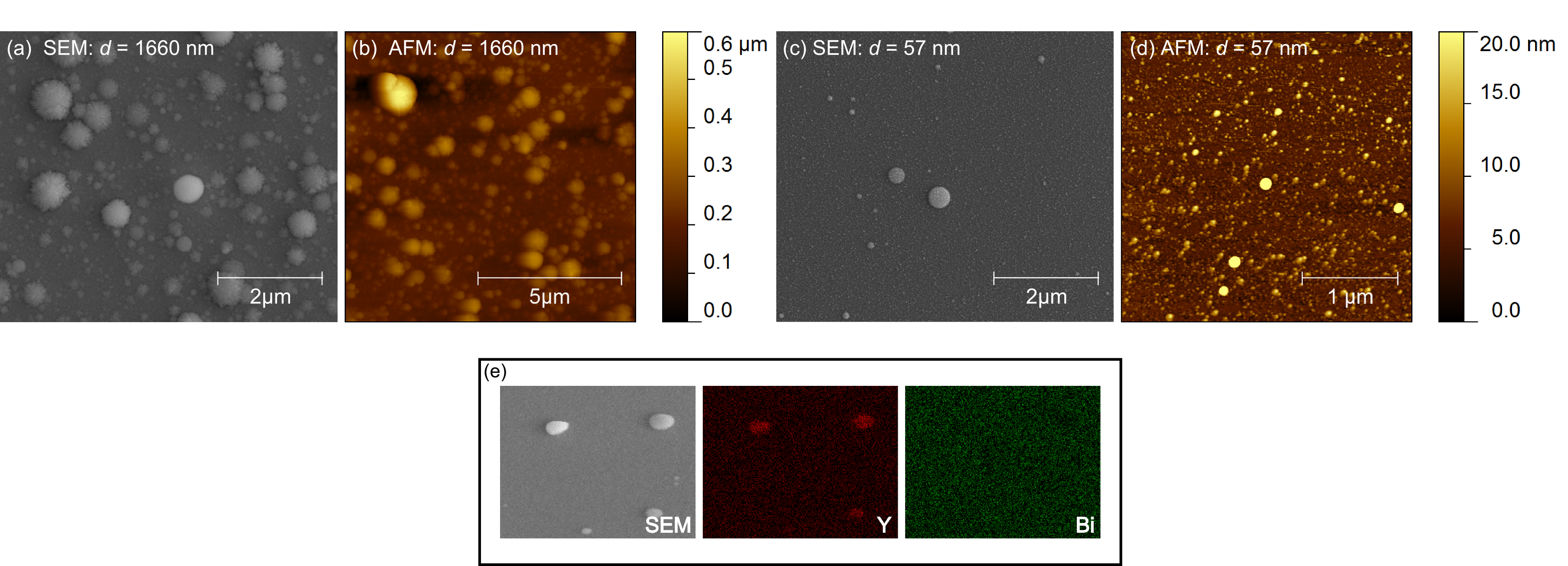
The surface morphology was investigated with a Park Systems XE-150 atomic force microscope (AFM) in dynamic non-contact mode and an FEI Novalab 200 scanning electron microscope (SEM). Topographic AFM images were post-processed with the Gwyddion software.Nečas and Klapetek (2012) Figure S2(a-d) shows topographic AFM and SEM images of the 1660 nm (a,b) and 57 nm (c,d) YBiO3 films A and B. The surface of film A is characterized by separate, very large crystalline grains with lateral dimensions around 700 nm and droplets. From the AFM image, a root-mean-squared (RMS) surface roughness of 55.8 nm is obtained. Droplet formation is also evident on the surface of film B (b) with an RMS surface roughness of 2.68 nm, and crystalline grain dimensions between 30 nm and 80 nm. The surface roughness and grain size are compatible with other YBiO3 films.(Li et al., 2007; Zhao et al., 2007; Pollefeyt et al., 2013) EDX analysis revealed that the droplets are mainly composed of yttrium. We argue, that the observed surface morphology can be explained by droplets and a mechanically soft target.
III Dielectric function
The dielectric function of YBiO3 was determined by means of standard variable angle spectroscopic reflection ellipsometry in the 0.03 eV to 4.5 eV spectral range applied to the two 1660 nm and 57 nm YBiO3 film samples A and B. For optically isotropic YBiO3, the measured quantities are the ellipsometric parameters and , which are defined by the ratio of the p- and s-polarized complex reflection coefficients and . A transfer matrix model is simultaneously adapted to the ellipsometry and optical transmission data to obtain a numerical B-spline model dielectric function of both YBiO3 films.Johs and Hale (2008) The measured and modeled and spectra of the 57 nm YBiO3 film are shown in Figure S3 (for film A see Fig. 3 of the main the text).
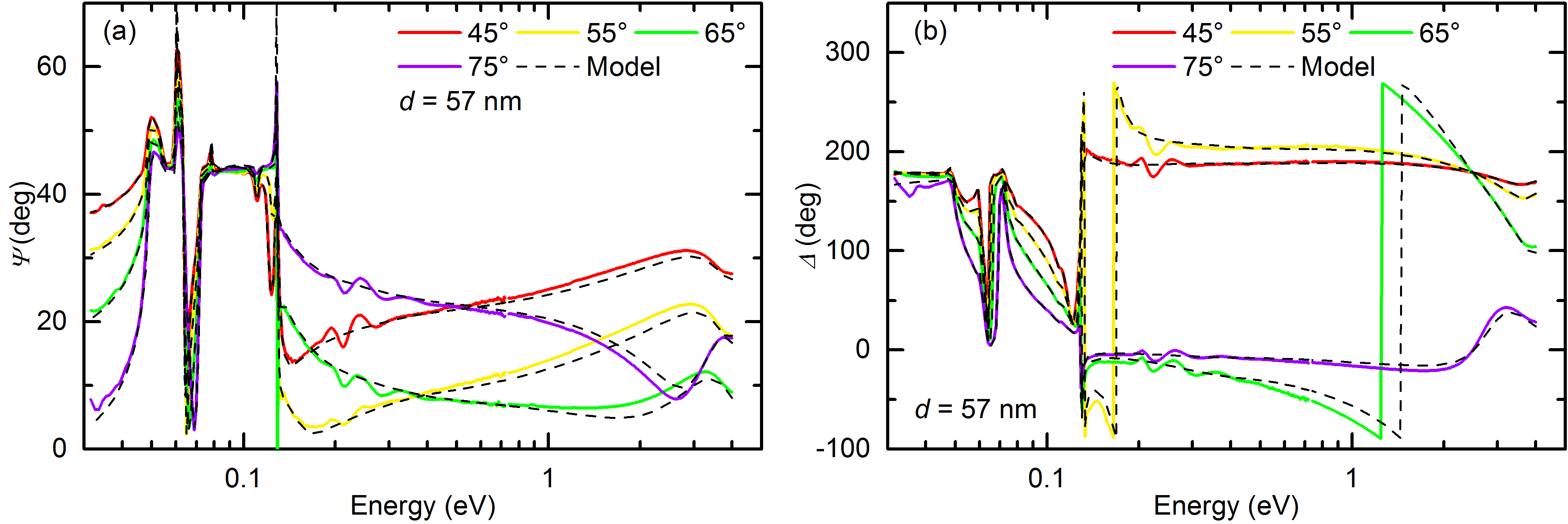
Figure S4 displays the calculated absorption coefficient obtained from the simultaneous modeling (cf. Fig. S3) and from individual models of YBiO3 films A and B, respectively. From the simultaneous modeling a direct bandgap of 3.6(1) eV was estimated. A similar result of 3.7 eV is obtained from the individual model of film B, which is however insensitive to absorption at lower energies. In contrast, film A is required to correctly reproduce absorption below about 3.3 eV, but is insensitive to absorption at higher energies. The model of film A furthermore exhibits an additional Urbach tail between 2.25 eV and 3.25 eV, as indicated by a straight line in the semi-log plot of ,Studenyak, Kranj, and Kurik (2014) Fig. S4(b). In summary, the simultaneous modeling of films A and B is required to reveal the direct and possible indirect bandgap in YBiO3.
References
- Li et al. (2007) G. Li, M. Pu, X. Du, Y. Zhang, H. Zhou, and Y. Zhao, Physica C: Superconductivity 452, 43 (2007).
- Zhao et al. (2007) Y. Zhao, M. Pu, G. Li, X. Du, H. Zhou, Y. Zhang, X. Yang, Y. Wang, R. Sun, and C. Cheng, Physica C: Superconductivity and its Applications 463-465, 574 (2007).
- Pollefeyt et al. (2013) G. Pollefeyt, S. Rottiers, P. Vermeir, P. Lommens, R. Hühne, K. De Buysser, and I. Van Driessche, Journal of Materials Chemistry A 1, 3613 (2013).
- Meiqiong et al. (2009) Y. Meiqiong, W. Xianhua, T. Yuancheng, and H. Junjun, Chinese Journal of Vacuum Science and Technology 29, 536 (2009).
- Jin et al. (2013) H. Jin, S. H. Rhim, J. Im, and A. J. Freeman, Scientific Reports 3, 1651 (2013).
- Trimarchi et al. (2014) G. Trimarchi, X. Zhang, A. J. Freeman, and A. Zunger, Physical Review B 90, 161111 (2014).
- Battle et al. (1983) P. D. Battle, C. R. A. Catlow, J. Drennan, and A. D. Murray, Journal of Physics C: Solid State Physics 16, L561 (1983).
- Battle et al. (1986) P. Battle, C. Catlow, J. Heap, and L. Moroney, Journal of Solid State Chemistry 63, 8 (1986).
- Kale, Jadhav, and Bichile (1999) K. V. Kale, K. M. Jadhav, and G. K. Bichile, Journal of Materials Science Letters 18, 9 (1999).
- Zhang et al. (2010) X. J. Zhang, W. T. Jin, S. J. Hao, Y. Zhao, and H. Zhang, Journal of Superconductivity and Novel Magnetism 23, 1011 (2010).
- de Putter (2014) R. de Putter, Towards stochiometric growth of YBiO3 thin films using pulsed laser deposition: a plasma approach, Master thesis, University of Twente (2014).
- Nečas and Klapetek (2012) D. Nečas and P. Klapetek, Open Physics 10, 181 (2012).
- Rietveld (1969) H. M. Rietveld, Journal of Applied Crystallography 2, 65 (1969).
- Nelson and Riley (1945) J. B. Nelson and D. P. Riley, Proceedings of the Physical Society 57, 160 (1945).
- Note (1) Assuming a cubic YBiO3(111) epilayer with Å, the lattice mismatch with the 13.00 5.50 Å2 -plane of Al2O3 will be +42 % and -40 %, respectively.
- Jellison et al. (1994) G. E. Jellison, L. A. Boatner, D. H. Lowndes, R. A. McKee, and M. Godbole, Applied Optics 33, 6053 (1994).
- Johs and Hale (2008) B. Johs and J. S. Hale, physica status solidi (a) 205, 715 (2008).
- Fujiwara (2007) H. Fujiwara, Spectrocopic ellipsometry: principles and applications (John Wiley & Sons, Chichester, England; Hoboken, NJ, 2007).
- Perdew (2009) J. P. Perdew, International Journal of Quantum Chemistry 28, 497 (2009).
- Fan et al. (2006) H. T. Fan, S. S. Pan, X. M. Teng, C. Ye, and G. H. Li, Journal of Physics D: Applied Physics 39, 1939 (2006).
- Zhang and Xiao (1998) S. Zhang and R. Xiao, Journal of Applied Physics 83, 3842 (1998).
- Studenyak, Kranj, and Kurik (2014) I. Studenyak, M. Kranj, and M. Kurik, International Journal of Optics and Applications 4, 76 (2014).