Nonlinear response of a ballistic graphene transistor with an ac-driven gate:
high harmonic generation and THz detection
Abstract
We present results for time-dependent electron transport in a ballistic graphene field-effect transistor with an ac-driven gate. Nonlinear response to the ac drive is derived utilizing Floquet theory for scattering states in combination with Landauer-Büttiker theory for transport. We identify two regimes that can be useful for applications: (i) low and (ii) high doping of graphene under source and drain contacts, relative to the doping level in the graphene channel, which in an experiment can be varied by a back gate. In both regimes, inelastic scattering induced by the ac drive can excite quasi-bound states in the channel that leads to resonance promotion of higher order sidebands. Already for weak to intermediate ac drive strength, this leads to a substantial change in the direct current between source and drain. For strong ac drive with frequency , we compute the higher harmonics of frequencies ( integer) in the source-drain conductance. In regime (ii), we show that particular harmonics (for instance ) can be selectively enhanced by tuning the doping level in the channel or by tuning the drive strength. We propose that the device operated in the weak-drive regime can be used to detect THz radiation, while in the strong-drive regime it can be used as a frequency multiplier.
I Introduction
Graphene for analogue high-frequency electronics has been the focus of intense research the last few years, and is one of the focus areas in the recently published graphene roadmapFerrari et al. (2015). Two-dimensionality of the material, high carrier mobility, gate-tunable charge density, and a unique band structure with massless Dirac electrons are a few of the properties that make graphene a promising material in this contextSchwierz (2010); Palacios et al. (2010); Glazov and Ganichev (2014); Otsuji et al. (2012); Koppens et al. (2014). Examples of devices already produced, with competitive figures of merits, are field-effect transistorsCheng et al. (2012), frequency doublersWang et al. (2009), frequency mixersHabibpour et al. (2012), and detectorsVicarelli et al. (2012); Mittendorff et al. (2013); Cai et al. (2014); Zak et al. (2014).
The electronic mobility has been constantly improving and ballistic electron transport is today studied intensively. Ballistic transport allows for development of massless Dirac electron optics, which is the graphene analogue of usual optics. Electron optics effects that have been observed include Fabry-Pérot interferences and snake statesRickhaus et al. (2015), Veselago lensingChen et al. (2016), and so-called whispering gallery modes in circular - junctionsZhao et al. (2015).
For ballistic devices, evidence of hydrodynamic behavior has been recently presented: viscous electron backflowBandurin et al. (2016) and breakdown of the Wideman-Franz lawCrossno et al. (2016); Ghahari et al. (2016). This indicates that due to the long elastic mean free path, and slow electron-phonon relaxation below room temperature, electron-electron interactions can be the most dominant scattering channel within a certain temperature window. However, at sufficiently low temperatures (below 100 K) electron-electron interactions also become weak and, ultimately, at lower temperature, transport is truly ballistic over long () length scales.
Improved mobility (possibly reaching ballistic transport) is a necessary condition for the development of high-frequency devices. There has therefore been a broad interest in the theory of time-dependent transport in graphene in the ballistic transport regime, including quantum pumpingPrada et al. (2009); Foa Torres et al. (2011); San-Jose et al. (2011, 2012), nonlinear electromagnetic responseMikhailov and Ziegler (2007, 2008); Syzranov et al. (2008); Calvo et al. (2012); Al-Naib et al. (2014); Sinha and Biswas (2012), and photon-assisted tunnelingTrauzettel et al. (2007); Zeb and Tahir (2008); Rocha et al. (2010); Savel’ev et al. (2012); Lu et al. (2012); Szabó et al. (2013); Zhu et al. (2015). In the non-classical regime, when the energy scale , set by the drive frequency ( is Planck’s constant divided by ), and the Fermi energy , measured relative to the charge-neutrality point, are of comparable magnitude, a variety of interesting quantum mechanical interference and resonance effects become important. In a recent paperKorniyenko et al. (2016) we have studied in detail a Fano resonanceBagwell and Lake (1992); Lu et al. (2012); Szabó et al. (2013); Zhu et al. (2015) induced by a quasibound bound state on the top gate barrier. We showed how it could be utilized to develop a frequency doubler for weak or moderate ac drive strength. In this paper we extend this study to include a more realistic doping profile across the device as well as strong ac drive. Within a fully quantum mechanical treatment based on Floquet theory and Landauer-Büttiker scattering theoryBagwell and Lake (1992); Pedersen and Büttiker (1998); Platero and Aguado (2004); Kohler et al. (2005), we show how Fano resonances as well as resonant tunneling can be utilized for detection of high-frequency radiation in the THz range or to generate high harmonics of the ac signal.
The outline of the paper is as follows. In Section II we give details of the model and the methods of calculations. This section also includes a characterization of the dc regime as a prologue to the discussions of time-dependent transport in the following chapter, as well as a detailed discussion of the relation between the different parameters of the model and various possible transport regimes. In Section III we present results for the weak ac drive regime, with focus on high-frequency radiation detection. In Section-IV we present result for the strong ac drive regime, with focus on high harmonic generation. Section V summarizes the paper. A few technical results are collected in the Appendix.
II Model
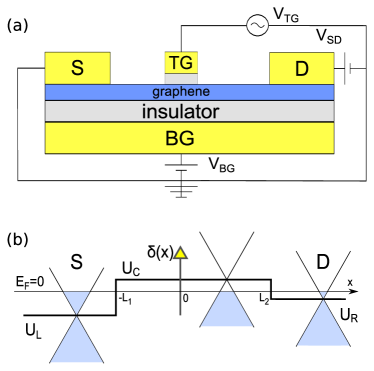
Our goal is to establish a relation between intrinsic electronic transport properties of a ballistic graphene transistor, depicted in Fig. 1(a), and experimentally controllable physical parameters. Extrinsic (parasitic) effects due to eventual surrounding circuit elements, must be dealt with when doing experiments, but can be neglected in an attempt to describe the intrinsic properties. We make a minimal model based on a number of assumptions that we outline in the following.
First, we assume that the contacts and gates are ideal, such that they can be described by the potential landscape sketched in Fig. 1(b). We take into account that the source and drain metallic contacts dope graphene underneath due to work function mismatches. The doping levels, set by and , in the graphene source and drain areas are thereby pinned Huard et al. (2008). On the other hand, in the transistor channel region, , the doping level can be tuned by the back gate potential. We define the channel Dirac point energy by setting (assuming absence of e-h puddles), where can be tuned by the back gate. Since we measure energies with respect to the Fermi level (aligned with the metallic contact Fermi energies), the Dirac point in the channel region is aligned with the Fermi energy for (the channel is then charge neutral). In summary, the doping profile sketched in Fig. 1(b) is given by
| (1) | |||||
We assume that the top gate is wide on the scale of the C-C bond length , but short on the scale that the envelope of the Dirac electron wavefunction varies, which is given by , where is the Fermi velocity. For energies near the Dirac point in the channel, we have . Based on the same arguments we assume that the doping level is changing slowly near the contacts on the scale but fast on the scale of . These assumptions mean that we can neglect intervalley scattering in the problem and consider only one valley. For transport quantities, a factor two for valley degeneracy is included in addition to the factor two for spin degeneracy. The above assumptions also allow us to use step functions for the doping profile, as in Eq. (1), and a delta barrier model for the top gate potential. The effective low-energy Hamiltonian then has the form
| (2) |
where we have set the Fermi velocity in graphene equal to unity, , and . The Pauli matrices in pseudo-spin space (A-B sublattices) are denoted by and . We assume the device to be very wide and translationally invariant along . Thus any edge effects are negligibly small and transverse momentum is (approximately) conserved. Above, and are respectively static and dynamic parts of the drive applied at the top gate. The delta function description of the top gate barrier is obtained as a limiting case of a very high and narrow square barrier, with the product (barrier strength) constant. Note that this theory for the Dirac quasiparticle envelope wavefunction holds as long as .
Wave function solutions have to satisfy the time-dependent Dirac equation
| (3) |
The harmonic potential, with frequency , in the Hamiltonian in Eq. (2) allows us to use a Fourier decomposition and construct a Floquet ansatz,
| (4) |
where amplitudes at sideband energies ( integer) are the result of the charge carrier picking up (or giving up) energy quanta from the oscillating barrier. The quasi-energy is set by the energy of the particle incident from the source electrode in the scattering problem. When plugged into Eq. (3) it yields a set of coupled differential equations for sideband amplitudes . The solutions can be derived in a straightforward manner by wavefunction matching and collected into a Floquet scattering matrix describing scattering of a quasiparticle incoming from left or right reservoir at energy and transverse momentum . We have collected all the key steps of the derivation in the Appendix. The reflection amplitudes are given in Eq. (66) and the transmission amplitudes are given in Eq. (67).
Following the Landauer-Büttiker scattering approach, the Floquet scattering matrix can be used to compute the time-dependent conductance between source and drain. The conductance is computed in linear response to the source-drain voltage , but in non-linear response to the oscillating top gate potential, described by its drive strength and frequency . The conductance is also a function of the static potential landscape, described by , as well as the static top gate potential quantified by its barrier strength . We derived the general formula for in Ref. Korniyenko et al., 2016. Here we choose to present results for the linear conductance in the right lead at , i.e. at the interface with the channel region. The expression for the conductance (per unit length in the transverse direction) at zero temperature is then111We note that for a system translationally invariant in the transverse direction, one has to compute conductance per unit length. In our previous work, c.f. Eqs. (D10)-(E2) in Ref. Korniyenko et al., 2016, we missed the prefactor associated with -integration in the current and conductance formulas, which we include here [see Eq. (7)]. The main results of Ref. Korniyenko et al., 2016 are not affected, although the scales in Fig. 3(b) and 4 should include this prefactor.
| (5) | |||||
| (6) | |||||
| (7) | |||||
where , , and are defined in Eq. (18). The factor with velocities appears here because we utilize a scattering basis where elementary waves in the leads carry unit probability flux. This guarantees that the scattering matrix coupling incoming and outgoing waves in the leads is unitary. The phase of the conductance components for is unimportant for our discussion and we will present results for below. Note that in the static case (i.e. ), the factor with velocities as well as the phase factor both reduce to unity and the usual Landauer-Büttiker formula for dc conductance simply in terms of transmission is obtained.
In the rest of the paper we shall report results for a symmetric setup with and symmetric doping profile . The transmission probabilities are computed for zero back gate voltage, i.e. , as a function of energy and transverse momentum parametrized by an impact angle . This means that corresponds to transmission at the Dirac point in the channel region. This is a conventional way to present transmission through a potential landscape. On the other hand, the zero-temperature linear conductance, computed via Eq. (7), shall be presented as a function of the channel doping (the position of the Dirac point energy ). In an experiment, the channel doping level can be tuned by the back gate voltage . Since the Fermi energy is pinned to the metallic source and drain contact Fermi energies, the radius of the Dirac cone in the graphene leads is constant, set by the doping level , while the radius in the channel is given by and varies with back gate voltage. This choice should correspond to the experimental situation.
II.1 dc characteristics
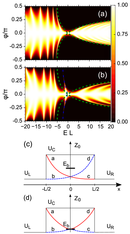
We start by analyzing the static case () in order to set the stage for the signatures of the time-dependent drive that we will study in the following sections. It is useful to first look at the case with no applied top gate potential , thereby highlighting the effect of the inhomogeneous doping profile. In fact, describes a square barrier across the channel of width . We plot the transmission probability in Fig. 2(a). The transmission amplitude is governed by pseudospin matching between regions with different doping. For small angles the mismatch is negligibly small, thus transmission approaches unity (Klein tunneling). The peaks in transmission for large angles and negative energies in Fig. 2(a) are analogous to Fabry-Pérot fringes, i.e. the result of wave interference between two partially reflecting mirrors (boundaries at the source and drain in this case). A typical fringe oscillation period is of the order of (reinstating the units). In addition to the two effects described above, there is a large region where transmission is largely suppressed. It occurs when the waves in the channel region are evanescent. Their longitudinal momentum component turns imaginary, giving us a condition on the critical angle of incidence ,
| (8) |
For any the waves injected from the electrodes are evanescent in the channel (). Note that Eq. (8) holds for . Otherwise there are no evanescent waves involved in transport and we may put . The boundary between propagating wave transport and evanescent wave transport is indicated by a green dashed line in Fig. 2(a). The evanescent wave factor lowers the transmission probability in general. However, for energies close to the Dirac point and small (or small ), this factor is still quite large and evanescent waves can reach between the two contacts thus giving rise to large transmission probability. Transport at is achieved exclusively through evanescent waves. This is the so-called pseudo-diffusive transport regime.Tworzydło et al. (2006)
When we introduce the static top gate delta barrier potential, , additional features appear in the transmission. First, the Fabry-Pérot oscillations are shifted due to an additional phase shift at the delta barrier, see Fig. 2(b). More importantly, the delta barrier can host one bound state at energy
| (9) |
that we studied for in Ref. Korniyenko et al., 2016. In that case, the bound state does not affect dc transport properties, but can be excited by ac drive. Here, for finite electrode doping , the bound state can be excited already in dc. In fact, in this case it is not a true bound state, rather a quasibound state with evanescent waves in the channel region connected to propagating waves in the leads. In Fig. 2(b) we see that the resonance in originates at and then disperses with the angle of incidence . The resonance can be understood in analogy with widely studied resonant double barrier tunnellingRicco and Azbel (1984); Yamamoto (1987) in Schrödinger quantum mechanics. In the analogy, the two barriers correspond in our case to the two channel regions between the contacts and the top gate delta barrier, and the resonant level between the barriers corresponds in our case to the quasibound state in the delta barrier. A complimentary point of view of the resonance can be found in the equations, see Appendix A.3. Off resonance, exponentially decaying waves with amplitudes and are connected, as sketched in Fig. 2(c). This results in an exponentially small transmission amplitude. On the other hand, when the quasibound state is hit, the exponentially decaying wave with amplitude on one side of the delta barrier is coupled only to exponentially rising solution with amplitude on the other side, as sketched in Fig. 2(d). The exponential functions thereby cancel in the expression for the transmission which leads to resonance behavior [c.f. Eq. (55)].
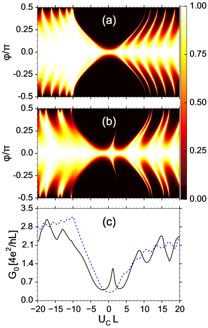
For the calculation of the conductance in Eq. (7) we need to integrate the transmission probability over angles. In an attempt to describe the typical experimental situation we assume that the Fermi energy in the device and the doping levels in the leads are pinned by the Fermi energy in the metal contacts, while the back gate can be used to tune the doping level in the channel. The zero-temperature conductance as a function of is then computed by integrating the transmission function over angles at fixed energy (Fermi energy) and fixed and . We plot the corresponding view of the angle-dependent transmission function in Fig. 3(a)-(b). Note that in Fig. 2 we plotted as a function of and for fixed and fixed and . The transmission function as viewed in Fig. 3(a)-(b) corresponds to leads that are electron-doped (here ). Thus, both incoming waves and scattered waves in the leads are electron-like (n-type) at the Fermi energy . For , we have electron-like waves at in the channel, while for we have hole-like waves in the channel (p-type). Therefore, the Fabry-Pérot interference patterns for positive (n-p-n junction) and negative (n-n’-n junction) are different.
In Fig. 3(c) we present the dc conductance as a function of channel doping level . For we have mainly evanescent mode transport, while for larger values of we find oscillations due to the Fabry-Pérot interferences. The resonance peak near (solid black line for finite ) is due to the delta barrier induced quasibound state.
II.2 Parameter regimes
| contact doping levels | |
|---|---|
| channel doping level | |
| channel length | |
| channel asymmetry | |
| drive frequency |
Starting from the dc characterization above, we can identify several parameter regimes. They can be described by different relations between the relevant energy scales in the problem, listed in Table 1. In the dc characterization above, we used as energy scale. Note that with , energies are measured in units of . In addition to the relations between the energy scales in Table 1, we have to take into account the oscillating delta barrier strength .
The observed regimes in dc are (c.f. Fig. 3)
-
I.
: propagating wave transport
-
(a)
: clearly visible Fabry-Pérot interferences as a function of with period approximately given by
-
(b)
: very fast oscillations that in reality would be washed out by inhomogeneity or temperature smearing
-
(c)
: the oscillations are too slow (on the scale of ) to be observed
-
(a)
-
II.
: evanescent wave transport (pseudo-diffusive regime)
-
(a)
: resonant tunneling is possible when the channel is not too asymmetric
-
(a)
The dc drive strength sets the position of the quasibound state in resonant tunneling regime and shifts the Fabry-Pérot oscillations, but does not define a regime by itself. We note that both the evanescent wave regimeDanneau et al. (2008) and the Fabry-Pérot regimeRickhaus et al. (2015) have been observed experimentally.
Under ac drive we will in the next sections investigate the following regimes:
-
III.
: Weak to intermediate drive
-
(a)
, low contact doping; with I.a above: Fano and Breit-Wigner resonances
-
(b)
, high contact doping; with II.a above: inelastic resonant tunneling
-
(a)
-
IV.
: Strong drive
-
(a)
, low contact doping; with I.a above: multiple Fano and Breit-Wigner resonances
-
(b)
, high contact doping; with II.a above: inelastic resonant tunneling and high-harmonic generation
-
(a)
We can estimate from experiments the typical parameter values. Contact doping (parameter ) has been reportedGiovannetti et al. (2008); Laitinen et al. (2016) in the range of -100 to 100 meV (corresponding to doping levels of up to cm-2, either or -type). Typical device channel lengths are from 10 nm to 1 m, making the corresponding energy scale in the range of meV. The corresponding ballistic flight time from source to drain is and is about 1 ps. We note in passing that within Landauer-Büttiker scattering theory, all relaxation times must then be longer than this, which is the case at low temperature and low energies in a ballistic device (mobility cm2/Vs). The driving frequency, , is between 0.4-40 meV for the THz frequency range THz. The drive strength , for , corresponds to a voltage of the order of a meV on the top gate for typical gate lengths (see the estimate in our previous paperKorniyenko et al. (2016)). Finally, in the following we assume that temperature is the smallest energy scale (we put ). With these numbers, all parameter regimes listed above are within experimental reach.
III Weak to intermediate drive,
III.1 Low contact doping: Fano and Breit-Wigner resonances
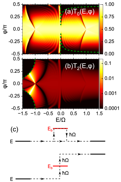
In Ref. Korniyenko et al., 2016 we studied the case when is the smallest energy scale, i.e the channel is long. We were then allowed to assume that evanescent waves can not reach between the contacts and the delta barrier. In practice we set , and let . In these limits, we studied Fano and Breit-Wigner resonances induced by the delta barrier quasibound state and argued that they can be used to enhance the second harmonic. In the more general formalism introduced here, we can ask the question what a small amount of contact doping leads to. We present in Fig. 4(a)-(b) the transmission probabilities and for a small amount of contact doping and large distance to contacts, . Compared with the results in Ref. Korniyenko et al., 2016 we find a small wedge of evanescent wave transport in an energy window around (outside the green dashed lines). The transmission of propagating waves displays fast Fabry-Pérot interferences. The Fano resonance in and the Breit-Wigner resonance in [processes sketched in Fig. 4(c)] are however not affected. For increasing contact doping (larger ), the Fabry-Pérot oscillations get stronger and will eventually interfere with the Fano and Breit-Wigner resonances, but not destroy them. This holds as long as . For shorter contacts, the wedge of evenescent wave transport around widens. When and are of comparable magnitude, the most important feature in the transmission is instead resonant inelastic tunneling.
III.2 High contact doping: inelastic resonant tunnelling
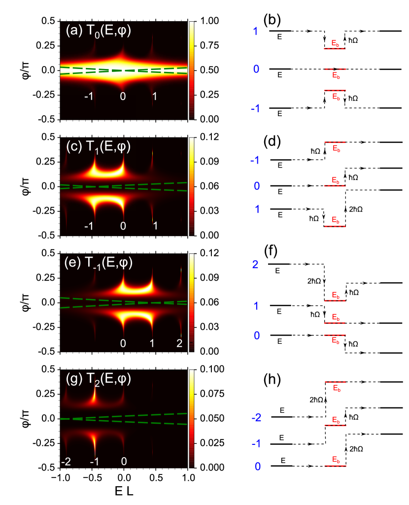
Let us next consider the resonant tunneling regime. We assume a symmetric device with , with highly doped leads, and weakly doped channel, , such that we have evanescent wave transport through the device. The resonance due to the quasibound state in the delta barrier studied for dc transport above will also create resonant inelastic tunneling under ac drive. The resonance condition for weak drive is . This leads to promotion of higher-order sidebands as well as higher harmonics in the conductance that we will study below.
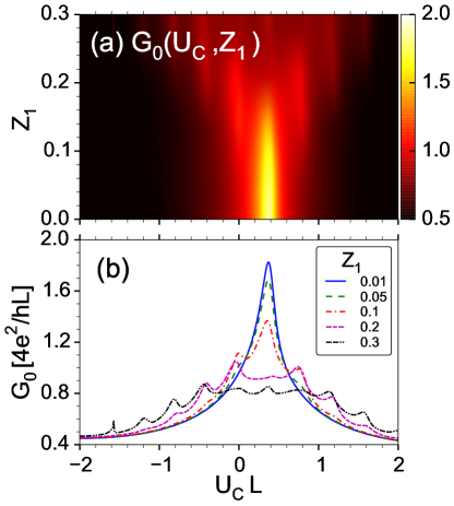
In Fig. 5 we present the transmission probabilities for , , and . For in Fig. 5(a) two new transmission peaks emerge, separated by from the main (0th) peak present already in dc. The side peaks emerge because of possibility of absorbing/emitting energy quanta, as shown in panel (b) of the figure. In the evanescent region, multiple sideband energies can now satisfy the bound state requirement, thus resulting in a number of resonant peaks separated roughly by (for ). Generally, these peaks are weaker than the one in the static case, since the bound state contribution is now spread across several channels. Analogous processes are involved during inelastic scattering between sidebands, as illustrated in Fig. 5(c) and (d) for , Fig. 5(e) and (f) for , and Fig. 5(g) and (h) for .
In Fig. 6 we present the dc conductance as a function of channel doping for increasing ac drive strength . The inelastic resonant tunneling processes discussed above for transmission probabilities result in side peaks in the conductance spaced by multiples of from the main resonance peak present in dc. Already for rather weak drive , several peaks are visible and the main elastic peak is reduced. This can be traced to the energy dependence in the matrix on the left-hand side in Eq. (67), which is given by a combination of functions in Eq. (18) all inversely proportional to energy. The bound state energy is small, which results in division of small numbers and enhanced effective coupling of sidebands close to the resonance energy. Thus, the range of validity of a perturbative approach in small is limited.
In the literature, when other systems than graphene have been studied, the conductance is often presented as a function of ac drive frequency Kohler et al. (2005). That is natural since there is often no knob corresponding to the very convenient back gate which can be used to tune the graphene channel doping level (i.e. the parameter varied above). For comparison, we present in Fig. 7 the dc conductance for varying frequency, keeping the doping level , i.e. a hole doped channel. In this case, we find conductance peaks at frequencies such that a sideband coincides with the quasibound state, i.e. . Higher order processes are weaker for weak drive strength , thus the resonance peaks have smaller amplitudes and widths.
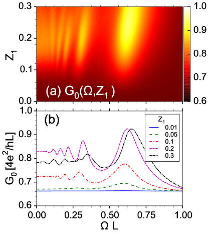
Considering Figs. 6-7 together, it is clear that the device can be used as a tunable detector. The frequency of the signal that needs to be detected tells us which channel doping we should choose (tunable by the back gate), such that the first sideband is resonant. Then the dc conductance is monitored to detect the signal.
IV Strong drive,
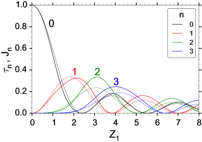
To understand the system behavior at strong drive it is useful to look at the transmission probability behavior as a function of driving strength . Since the barrier boundary condition matrix is directly related to Bessel functions of the first kind in sideband space, see Eq. (92), we can expect transmission amplitudes to also follow corresponding Bessel functions. To illustrate the point, we introduce normalized angle-integrated transmissions
| (10) |
Indeed, the general behavior of for constant follows that of , see Fig. 8. Next, let us discuss how the resonances described above for weak drive evolve for strong drive, bearing in mind that the distribution of sideband amplitudes is in simplified terms given by Bessel functions.
IV.1 Low contact doping
First, we would like to discuss the evolution of Fano and Breit-Wigner resonances described above for low doping of contacts. We observe multiple Fano resonances, c.f. Fig. 9, that are due to the bound state condition satisfied by sideband waves in the contacts. It is useful to note, that since we fixed the energy and have as our parameter, the evanescent wave region boundaries for sideband become horizontal lines given by where
| (11) |
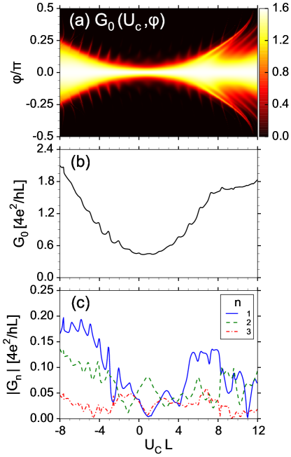
Note that this equation holds for . Otherwise waves are propagating in the contacts for all and we can set . To avoid confusion, we emphasize that in Eq. (11) defines critical angles for evanescent sideband waves in the contacts (which do not contribute to transport), while in Eq. (8) defines a critical angle for evanescent waves in the channel (which do contribute to transport). For parameters used in Fig. 9, only and sidebands have evanescent regions. Corresponding Fano and Breit-Wigner resonances now originate at the critical angle boundary and disperse with the angle of incidence. As has been shown in our previous work Korniyenko et al. (2016), Fano resonances broaden as and their positions change as the driving strength is increased. We note also that due to the strong coupling between sidebands for , the evanescent region boundary is clearly visible across all transmission channels. Unlike in the weak driving case, the zeroth transmission channel stops being dominant and thus higher sidebands are increasingly important in the conductance calculation.
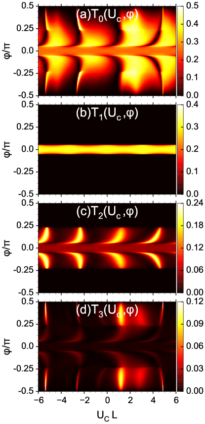
Given the strong separation between evanescent and propagating wave regions as a function of angles in transmissions, it leads to a similar pronounced behaviour in angle resolved conductances, as shown in Fig. 10(a) for the dc component. After integration over angles, we observe clear oscillations in the -dependence of the dc conductance, see Fig. 10(b), which are due to the multiple Fano resonances discussed above. The second and third harmonics are of equal size as the first harmonic for corresponding to the resonances, see Fig. 10(c).
It is useful to define a quantitative estimate of the relative power of ac harmonics as
| (12) |
For simplicity we exclude negative harmonics in this estimate, since we know that . In Ref. Korniyenko et al., 2016 we discussed weak drive and second harmonic generation. In Fig. 10(d) we show for strong drive that both second and third harmonic can be resonantly enhanced and become of the same order as the first harmonic for the case . Higher harmonics are however not enhanced above the first harmonic in the regime of low contact doping , even for stronger , because the multiple resonances are not equidistant in energy space.
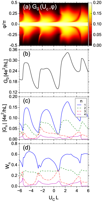
IV.2 High contact doping
Next, let us study the effect of strong contact doping ( large). See Fig. 11(a) for the angular dependence of the dc conductance in this case. A clear valley in the dc conductance is centered at the Dirac point in the central region (i.e. around ), which corresponds to evanescent wave transport in the channel. The double-barrier inelastic tunneling resonances at result in a fine comb of equidistant peaks inside the valley. After integration over angles, see Fig. 11(b), the dc conductance shows small oscillations related to the inelastic tunneling processes. Note that the weight of the resonance peak we studied in the absence of ac drive () in Fig. 3(b), has been completely redistributed across the many peaks of the comb. The peak period () is the same for all transmission channels. Therefore, analogical fine oscillations show up in ac harmonics as well, see Fig. 11(c).
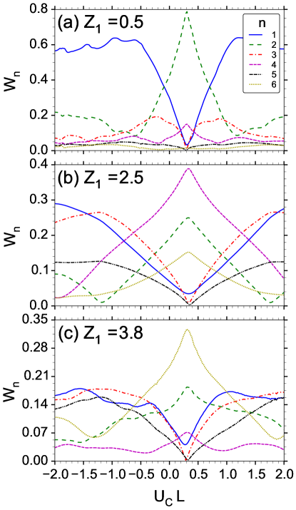
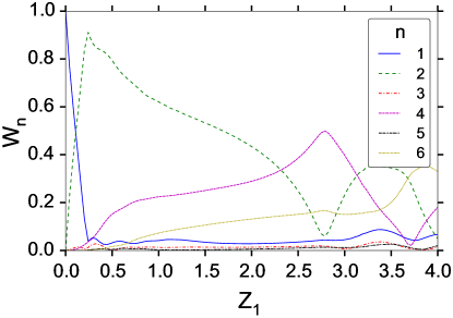
In Fig. 11(c) we note that for corresponding to the direct double-barrier resonance, the second harmonic is enhanced above the first harmonic, which is suppressed. By tuning parameters, we can in fact enhance a selected even harmonic, as shown in Fig. 12, where we present the weights as a function of channel doping for increasing drive strength . In panels (a)-(c) we obtain the , , and harmonic, respectively. To emphasize this result, we plot the distribution between harmonics roughly on resonance () as a function of in Fig. 13. In the whole range of drive strengths , all odd harmonics are suppressed, while even harmonics are enhanced, one after the other.
For weak drive strength , we can show that is suppressed while is enhanced through destructive (for ) and constructive (for ) interferences between the transmission processes responsible for the corresponding harmonic, c.f. Eq. (7). To explain this behavior, we first note that Eq. (91) tells us that sideband amplitudes are proportional to to lowest order in . For instance and (symmetric). It follows that for small the first conductance harmonic (before integration over transverse momentum) can be written as a sum of two terms involving two different transfer processes:
| (13) | |||||
where are complex numbers. On resonance, , the two terms cancel, and is suppressed. That this symmetry appears on resonance can be seen from Fig. 5, where the peaks in [panels (c) and (e)], corresponding to processes labeled 0 [panels (d) and (f)], have the same shape and magnitude. Off resonance, the probabilities are obviously not equal, the two terms do not cancel, and is not suppressed. For the enhancement of the second harmonic, we note that for small we have . All terms consist of real products of the coupling matrix elements in sideband space. On resonance, for instance with , and the two terms sum up constructively because of the real coupling in sideband space. For stronger drive, the odd (even) harmonics are suppressed (enhanced) in an analogous way, where pairs of processes add up destructively (constructively).
V Summary
We have presented results for the ac conductance in a ballistic graphene field-effect transistor with a time-modulated top gate potential, including an inhomogeneous doping profile across the device. We have studied two regimes, corresponding to (i) low doping of contacts and (ii) high doping of contacts, relative to the doping level in the channel (which is tunable by a back gate). For case (i) we find Fano resonances in direct transmission and Breit-Wigner resonances in inelastic scattering to sideband energies. The resonances are due to excitation of quasibound states in the channel, analogous to what we found in Ref. Korniyenko et al., 2016. Here we have shown that these resonances survive when a moderately varying doping landscape across the device is taken into account. For case (ii) we find inelastic tunneling resonances via quasibound states in the top gate barrier potential. For weak drive, the resonances lead to a large response in the direct current between source and drain already for weak ac drive on the top gate. We propose that the device can be utilized as a detector in the THz frequency range. In addition, for strong drive, inelastic tunneling to multiple sidebands results in resonant excitation of higher harmonics [we demonstrate dominance of in Fig. 12(c)], with an even number due to an interference effect between different tunneling processes. The harmonic (even) can be selected either by the back gate or by tuning the drive strength. In summary, ac transport in ballistic graphene field-effect transistors is a rich subject for studying quantum mechanical resonance phenomena that can possibly also be utilized in applications such as detectors of THz radiation or to generate high harmonics.
Acknowledgements.
We acknowledge financial support from the Swedish foundation for strategic research (SSF), the Knut and Alice Wallenberg foundation (KAW), and the Swedish research council. The research of OS was partly supported by the National Science Foundation (Grant DMR-1508730).Appendix A Wave solutions - static case
First we derive the wave solutions to the Dirac equation without time-dependent perturbation. We assume translational invariance and conserved parallel momentum , in which case the Hamiltonian has the form
| (14) |
where the device doping profile is described by
| (15) |
This means that in this derivation we choose the Dirac point in the device channel, , as reference level where (i.e. ). The static Dirac equation
| (16) |
is straightforward to solve by making a plane-wave ansatz and find unknown coefficients through boundary conditions. But first it is convenient to introduce a scattering basis.
A.1 Scattering basis
Consider the homogeneous case, i.e. and in Eq. (14). The solutions, labeled by and , can be organized into a scattering basis for right- and left-moving (along the -axis) plane waves, as defined by their group velocities. This scattering basis has the form
| (17) |
where
| (18) | |||
The normalization of these plane waves is such that they carry unit probability flux along the -axis, defined as
| (19) |
That is, we have and . This scattering basis is useful in deriving the scattering matrix and computing the current within the Landauer-Büttiker formalism, as we described in detail in Ref. Korniyenko et al., 2016 for the case .
A.2 Scattering matrix derivation
Below we solve the scattering problem for quasiparticles at energy injected from the left contact at conserved transverse momentum given by
| (20) |
where is the incidence angle on the scattering region, measured with respect to the -axis. There are four regions in our device: left and right contacts labeled and and left and right channel regions (with respect to the delta potential barrier) labeled and . The scattering state ansatz si then
| (21) |
Note that the doping level in the channel region () is different from that in the contacts ( and ). As a consequence, the waves can be evanescent in the channel region. This is included in the ansatz above by allowing in Eq. (18) to be imaginary. The convention we use is that denotes a wave evanescent towards positive , while denotes a wave evanescent in the opposite direction. This means that if and turns imaginary, the ansatz above also holds, although in this case is not a transmission amplitude. It is then eliminated in favor of the reflection coefficient , with . This is not so important in the present discussion, but becomes important in the following section on ac transport. In the main text we only consider the special case for simplicity.
The coefficients in Eq. (21) are found through the boundary conditions, which are simple wave continuity at and , and a pseudospin rotation operation at the delta barrier (c.f. Ref. Korniyenko et al., 2016):
| (22) | |||||
| (23) | |||||
| (24) |
From Eq. (24) we can obtain and in terms of
| (25) | |||||
| (26) |
Note that , and analogous for and (also, , etc. appearing below are computed at energy ). The quantities in regions and , computed at energy , lack superscripts. Above and in the following we suppress the explicit reference to the dependences on and unless necessary.
A.3 Double barrier tunneling
Since waves are always propagating inside the delta potential, the channel regions on either side of it form a double tunnel barrier when lead regions are highly doped such that waves are propagating there as well. It is well-known that the bound state in this structure can lead to resonances in the transmission amplitude derived above. To understand it qualitatively we write down a propagation matrix that relates amplitudes and at the left edge of the channel to amplitudes and at the right edge, see Fig. 2, i.e.
| (36) |
where
| (37) |
The four elements of the -matrix are obtained from the boundary condition at the delta barrier Eq. (23) as
| (41) | |||
| (45) | |||
| (49) | |||
| (53) |
For the case of evanescent waves in the channel, the wavevector becomes imaginary and Eq. (37) takes the form
| (54) |
where and .
For a symmetric system with , and on resonance, i.e. when the energy of the scattering state coincides with the delta barrier bound state , it follows from the derivation in Ref. Korniyenko et al., 2016 [c.f. Eq. (B4)] that . When that happens, we see that Eq. (36) with Eq (54) leads to
| (55) | |||
| (56) |
where we also noted that . This shows the cross connection between decaying and exploding solutions illustrated in Fig. 2(d). When transmission is enhanced to unity, the exponential functions due to tunneling through the two barriers cancel each other. Off resonance, this clean-cut cross connection does not occur and the transmission is exponentially suppressed.
Appendix B Wave solutions - dynamic case
Let us now derive the Floquet scattering matrix in presence of an oscillating delta barrier. The Hamiltonian we consider is
| (57) |
The time-dependent Dirac equation
| (58) |
including a time-periodic potential as in Eq. (57), can be solved by making use of the Floquet ansatz:
| (59) |
In analogy with the static case above, this ansatz is made in each region. Coefficients for transmitted and reflected waves are then contained in the amplitudes . The coefficients are determined through the boundary conditions. A complication in the dynamic case is the boundary condition at the oscillating delta barrier, which mixes amplitudes at different sideband energies . Following Ref. Korniyenko et al., 2016, the boundary condition is best formulated by first introducing a column vector with the many sideband amplitudes ,
| (60) |
The condition to be satisfied at is then
| (61) | |||
The barrier scatters an incident wave labeled by and into a linear combination of waves labeled by and . In the end, when calculating transport properties, we have to consider only propagating outgoing waves in the leads, and . We use the following ansatz:
| (62) |
The three boundary conditions can be written as
| (63) | |||||
| (64) | |||||
| (65) |
The steps to solve for the coefficients are analogous to the static case and we do not present them here. The resulting transmission and reflection amplitudes are computed from
| (66) | |||
| (67) |
where
| (72) | |||||
| (77) | |||||
| (82) |
This system of equations for reduces for the static case (then only is relevant) to Eq. (33). For the case of no contact doping of the leads, i.e. , these equations reduce to Eq. (B14) in Ref. Korniyenko et al., 2016.
Appendix C Boundary condition Bessel function expansion
In this section we show that the boundary condition at the oscillating delta barrier in Eq. (61) can be rewritten in terms of Bessel-functions of the first kind. The matrix elements in Eq. (67) for transmission amplitudes, which determines the strength of sideband coupling, thereby decay with increasing as .
The tensor in Eq. (61) that represents the boundary condition at the delta barrier can be written as,
| (83) |
We will rewrite it to highlight the sideband space distribution. We will start by expanding the ac part of it in a Taylor series,
| (84) |
Let us study the off-diagonal matrix taken to the ’th power, i.e. . Its matrix elements are given by binomial coefficients
| (85) |
where . Matrix elements for are zero. Let us now introduce a matrix with unity entries on its ’th diagonals,
| (86) |
Note that and in Eq. (83) are included in this definition. Then we can rewrite Eq. (85) by setting . We obtain
| (87) |
The Taylor series is therefore given by
| (88) |
By introducing a substitution we can rewrite it in a more convenient form
| (89) |
Using the Bessel function of the first kind series representation,
| (90) |
we arrive at
| (91) |
Including the dc prefactor, we arrive at
| (92) |
References
- Ferrari et al. (2015) A. C. Ferrari et al., “Science and technology roadmap for graphene, related two-dimensional crystals, and hybrid systems,” Nanoscale 7, 4598–4810 (2015).
- Schwierz (2010) F. Schwierz, “Graphene transistors,” Nature Nanotechnology 5, 487–496 (2010).
- Palacios et al. (2010) T. Palacios, A. Hsu, and H. Wang, “Applications of Graphene Devices in RF Communications,” Ieee Communications Magazine 48, 122–128 (2010).
- Glazov and Ganichev (2014) M. M. Glazov and S. D. Ganichev, “Physics Reports,” Physics Reports-Review Section Of Physics Letters 535, 101–138 (2014).
- Otsuji et al. (2012) T. Otsuji, S. A. Boubanga Tombet, A. Satou, H. Fukidome, M. Suemitsu, E. Sano, V. Popov, M. Ryzhii, and V. Ryzhii, “Graphene materials and devices in terahertz science and technology,” MRS Bulletin 37, 1235–1243 (2012).
- Koppens et al. (2014) F. H. L. Koppens, T. Mueller, P. Avouris, A. C. Ferrari, M. S. Vitiello, and M. Polini, “Photodetectors based on graphene, othertwo-dimensional materials and hybrid systems,” Nature Nanotechnology 9, 780–793 (2014).
- Cheng et al. (2012) R. Cheng, J. Bai, L. Liao, H. Zhou, Y. Chen, L. Liu, Y.-C. Lin, S. Jiang, Y. Huang, and X. Duan, “High-frequency self-aligned graphene transistors with transferred gate stacks,” Proceedings Of The National Academy Of Sciences Of The United States Of America 109, 11588–11592 (2012).
- Wang et al. (2009) H. Wang, D. Nezich, J. Kong, and T. Palacios, “Graphene Frequency Multipliers,” IEEE Electron Device Letters 30, 547–549 (2009).
- Habibpour et al. (2012) O. Habibpour, S. Cherednichenko, J. Vukusic, K. Yhland, and J. Stake, “A Subharmonic Graphene FET Mixer,” IEEE Electron Device Letters 33, 71–73 (2012).
- Vicarelli et al. (2012) L. Vicarelli, M. S. Vitiello, D. Coquillat, A. Lombardo, A. C. Ferrari, W. Knap, M. Polini, V. Pellegrini, and A. Tredicucci, “Graphene field-effect transistors as room-temperature terahertz detectors,” Nature Materials 11, 865–871 (2012).
- Mittendorff et al. (2013) M. Mittendorff, S. Winnerl, J. Kamann, J. Eroms, D. Weiss, H. Schneider, and M. Helm, “Ultrafast graphene-based broadband THz detector,” Applied Physics Letters 103, 021113 (2013).
- Cai et al. (2014) X. Cai, A. B. Sushkov, R. J. Suess, M. M. Jadidi, G. S. Jenkins, L. O. Nyakiti, R. L. Myers-Ward, S. Li, J. Yan, D. K. Gaskill, T. E. Murphy, H. D. Drew, and M. S. Fuhrer, “Sensitive room-temperature terahertz detectionvia the photothermoelectric effect in graphene,” Nature Nanotechnology 9, 814 –819 (2014).
- Zak et al. (2014) A. Zak, M. A. Andersson, M. Bauer, J. Matukas, A. Lisauskas, H. G. Roskos, and J. Stake, “Antenna-Integrated 0.6 THz FET Direct Detectors Based on CVD Graphene,” Nano Letters 14, 5834–5838 (2014).
- Rickhaus et al. (2015) P. Rickhaus, P. Makk, M.-H. Liu, E. Tovari, M. Weiss, R. Maurand, K. Richter, and C. Schönenberger, “Snake trajectories in ultraclean graphene p–n junctions,” Nature Communications 6, 1–6 (2015).
- Chen et al. (2016) S. Chen, Z. Han, M. M. Elahi, K. M. M. Habib, L. Wang, B. Wen, Y. Gao, T. Taniguchi, K. Watanabe, J. Hone, A. W. Ghosh, and C. R. Dean, “Electron optics with ballistic graphene junctions,” arXiv.org (2016), 1602.08182v1 .
- Zhao et al. (2015) Y. Zhao, J. Wyrick, F. D. Natterer, J. F. Rodriguez-Nieva, C. Lewandowski, K. Watanabe, T. Taniguchi, L. S. Levitov, N. B. Zhitenev, and J. A. Stroscio, “Creating and probing electron whispering-gallery modes in graphene,” Science (New York, NY) 348, 672–675 (2015).
- Bandurin et al. (2016) D. A. Bandurin, I. Torre, R. K. Kumar, M. Ben Shalom, A. Tomadin, A. Principi, G. H. Auton, E. Khestanova, K. S. Novoselov, I. V. Grigorieva, L. A. Ponomarenko, A. K. Geim, and M. Polini, “Negative local resistance caused by viscous electron backflow in graphene,” Science (New York, NY) 351, 1055–1058 (2016).
- Crossno et al. (2016) J. Crossno, J. K. Shi, K. Wang, X. Liu, A. Harzheim, A. Lucas, S. Sachdev, P. Kim, T. Taniguchi, K. Watanabe, T. A. Ohki, and K. C. Fong, “Observation of the Dirac fluid and the breakdown of the Wiedemann-Franz law in graphene,” Science (New York, NY) 351, 1058–1061 (2016).
- Ghahari et al. (2016) F. Ghahari, H.-Y. Xie, T. Taniguchi, K. Watanabe, M. S. Foster, and P. Kim, “Enhanced Thermoelectric Power in Graphene: Violation of the Mott Relation by Inelastic Scattering,” Physical Review Letters 116, 136802 (2016).
- Prada et al. (2009) E. Prada, P. San-Jose, and H. Schomerus, “Quantum pumping in graphene,” Physical Review B 80, 245414 (2009).
- Foa Torres et al. (2011) L. E. F. Foa Torres, H. L. Calvo, C. G. Rocha, and G. Cuniberti, “Enhancing single-parameter quantum charge pumping in carbon-based devices,” Applied Physics Letters 99, 092102 (2011).
- San-Jose et al. (2011) P. San-Jose, E. Prada, S. Kohler, and H. Schomerus, “Single-parameter pumping in graphene,” Physical Review B 84, 155408 (2011).
- San-Jose et al. (2012) P. San-Jose, E. Prada, H. Schomerus, and S. Kohler, “Laser-induced quantum pumping in graphene,” Applied Physics Letters 101, 153506 (2012).
- Mikhailov and Ziegler (2007) S. A. Mikhailov and K. Ziegler, “New Electromagnetic Mode in Graphene,” Physical Review Letters 99, 016803 (2007).
- Mikhailov and Ziegler (2008) S. A. Mikhailov and K. Ziegler, “Nonlinear electromagnetic response of graphene: frequency multiplication and the self-consistent-field effects,” Journal Of Physics-Condensed Matter 20, 384204 (2008).
- Syzranov et al. (2008) S. V. Syzranov, M. V. Fistul, and K. B. Efetov, “Effect of radiation on transport in graphene,” Physical Review B 78, 045407 (2008).
- Calvo et al. (2012) H. L. Calvo, P. M. Perez-Piskunow, S. Roche, and L. E. F. Foa Torres, “Laser-induced effects on the electronic features of graphene nanoribbons,” Applied Physics Letters 101, 253506 (2012).
- Al-Naib et al. (2014) I. Al-Naib, J. E. Sipe, and M. M. Dignam, “High harmonic generation in undoped graphene: Interplay of inter- and intraband dynamics,” Physical Review B 90, 245423 (2014).
- Sinha and Biswas (2012) C. Sinha and R. Biswas, “Transmission of electron through monolayer graphene laser barrier,” Applied Physics Letters 100, 183107 (2012).
- Trauzettel et al. (2007) B. Trauzettel, Y. M. Blanter, and A. F. Morpurgo, “Photon-assisted electron transport in graphene: Scattering theory analysis,” Physical Review B 75, 035305 (2007).
- Zeb and Tahir (2008) M. A. Zeb and M. Tahir, “Chiral tunneling through a time-periodic potential in monolayer graphene,” Physical Review B 78, 1–7 (2008).
- Rocha et al. (2010) C. G. Rocha, L. E. F. F. Torres, and G. Cuniberti, “ac transport in graphene-based Fabry-Pérot devices,” Physical Review B 81, 115435 (2010).
- Savel’ev et al. (2012) S. E. Savel’ev, W. Häusler, and P. Hänggi, “Current Resonances in Graphene with Time-Dependent Potential Barriers,” Physical Review Letters 109, 226602 (2012).
- Lu et al. (2012) W.-T. Lu, S.-J. Wang, W. Li, Y.-L. Wang, C.-Z. Ye, and H. Jiang, “Fano-type resonance through a time-periodic potential in graphene,” Journal Of Applied Physics 111, 103717 (2012).
- Szabó et al. (2013) L. Z. Szabó, M. G. Benedict, A. Czirják, and P. Földi, “Relativistic electron transport through an oscillating barrier: Wave-packet generation and Fano-type resonances,” Physical Review B 88, 075438 (2013).
- Zhu et al. (2015) R. Zhu, J.-H. Dai, and Y. Guo, “Fano resonance in the nonadiabatically pumped shot noise of a time-dependent quantum well in a two-dimensional electron gas and graphene,” Journal Of Applied Physics 117, 164306 (2015).
- Korniyenko et al. (2016) Y. Korniyenko, O. Shevtsov, and T. Löfwander, “Resonant second-harmonic generation in a ballistic graphene transistor with an ac-driven gate,” Physical Review B 93, 035435 (2016).
- Bagwell and Lake (1992) P. Bagwell and R. Lake, “Resonances in transmission through an oscillating barrier,” Physical Review B 46, 15329–15336 (1992).
- Pedersen and Büttiker (1998) M. H. Pedersen and M. Büttiker, “Scattering theory of photon-assisted electron transport,” Physical Review B 58, 12993–13006 (1998).
- Platero and Aguado (2004) G. Platero and R. Aguado, “Photon-assisted transport in semiconductor nanostructures,” Physics Reports-Review Section Of Physics Letters 395, 1–157 (2004).
- Kohler et al. (2005) S. Kohler, J. Lehmann, and P. Hänggi, “Driven quantum transport on the nanoscale,” Physics Reports-Review Section Of Physics Letters 406, 379–443 (2005).
- Huard et al. (2008) B. Huard, N. Stander, J. A. Sulpizio, and D. Goldhaber-Gordon, “Evidence of the role of contacts on the observed electron-hole asymmetry in graphene,” Physical Review B 78, 121402 (2008).
- Note (1) We note that for a system translationally invariant in the transverse direction, one has to compute conductance per unit length. In our previous work, c.f. Eqs. (D10)-(E2) in Ref. \rev@citealpnumKorniyenko:2016ct, we missed the prefactor associated with -integration in the current and conductance formulas, which we include here [see Eq. (7)]. The main results of Ref. \rev@citealpnumKorniyenko:2016ct are not affected, although the scales in Fig. 3(b) and 4 should include this prefactor.
- Tworzydło et al. (2006) J. Tworzydło, B. Trauzettel, M. Titov, A. Rycerz, and C. Beenakker, “Sub-Poissonian Shot Noise in Graphene,” Physical Review Letters 96, 246802 (2006).
- Ricco and Azbel (1984) B. Ricco and M. Y. Azbel, “Physics of resonant tunneling. The one-dimensional double-barrier case,” Physical review. B, Condensed matter 29, 1970–1981 (1984).
- Yamamoto (1987) H. Yamamoto, “Resonant tunneling condition and transmission coefficient in a symmetrical one-dimensional rectangular double-barrier system,” Applied Physics A Solids and Surfaces 42, 245–248 (1987).
- Danneau et al. (2008) R. Danneau, F. Wu, M. F. Craciun, S. Russo, M. Y. Tomi, J. Salmilehto, A. F. Morpurgo, and P. J. Hakonen, “Shot Noise in Ballistic Graphene,” Phys Rev Lett 100, 196802 (2008).
- Giovannetti et al. (2008) G. Giovannetti, P. A. Khomyakov, G. Brocks, V. M. Karpan, J. Van Den Brink, and P. J. Kelly, “Doping Graphene with Metal Contacts,” Physical Review Letters 101, 026803 (2008).
- Laitinen et al. (2016) A. Laitinen, G. S. Paraoanu, M. Oksanen, M. F. Craciun, S. Russo, E. Sonin, and P. Hakonen, “Contact doping, Klein tunneling, and asymmetry of shot noise in suspended graphene,” Physical Review B 93, 115413 (2016).