Zero-line modes at stacking faulted domain walls in multilayer graphene
Abstract
Rhombohedral multilayer graphene is a physical realization of the chiral two-dimensional electron gas that can host zero-line modes (ZLMs), also known as kink states, when the local gap opened by inversion symmetry breaking potential changes sign in real space. Here we study how the variations in the local stacking coordination of multilayer graphene affects the formation of the ZLMs. Our analysis indicates that the valley Hall effect develops whenever an interlayer potential difference is able to open up a band gap in stacking faulted multilayer graphene, and that ZLMs can appear at the domain walls separating two distinct regions with imperfect rhombohedral stacking configurations. Based on a tight-binding formulation with distant hopping terms between carbon atoms, we first show that topologically distinct domains characterized by the valley Chern number are separated by a metallic region connecting AA and AA′ stacking line in the layer translation vector space. We find that gapless states appear at the interface between the two stacking faulted domains with different layer translation or with opposite perpendicular electric field if their valley Chern numbers are different.
I Introduction
Rhombohedral graphene multilayers may host one-dimensional metallic states at the domain wall between two broken inversion symmetry insulating regions with opposite mass signs either due to reversal of sign of the perpendicular electric field (Martin et al., 2008; Jung et al., 2011; Bi et al., 2015; Zhang et al., 2013; de Sena et al., 2014) or reversal of stacking order (Semenoff et al., 2008; Vaezi et al., 2013; Zhang et al., 2013; Jung et al., 2012). As a rule of thumb, at the interface between two domains made by -layer rhombohedral graphene, the co-propagating gapless metallic states appear in each valley inside the bulk gap along the interface Jung et al. (2011); Volovik (2003); Yao et al. (2009), whose origin can be traced back to the valley Hall effect (Bi et al., 2015; Jung et al., 2011, 2012; Vaezi et al., 2013; Zhang et al., 2013) associated with opposite Hall conductivities at each valley (Xiao et al., 2007). Theoretically it was predicted that the zero-line modes (ZLMs), also known as kink states Jung et al. (2011); Killi et al. (2012); Vaezi et al. (2013), will have exceptional transport properties such as suppressed backscattering, zero bend resistance, and chirality encoded current filtering (Qiao et al., 2011, 2014), and have been proposed as splitters of Cooper pairs injected by superconducting electrodes (Schroer et al., 2015). There has been recently a number of experimental advancements related to the ZLMs in bilayer graphene. The enhanced electron density signals at tilted boundaries due to stacking faults in bilayer graphene were visualized through transmission electron microscopy measurements (Alden et al., 2013), confirming the theoretical expectations of finding stacking-dependent ZLMs at the stacking domain walls (Vaezi et al., 2013). Recently a direct observation of the ZLMs at AB/BA tilted boundaries in bilayer graphene through infrared nanoscopy and subsequent measurement of ballistic transport has been reported (Ju et al., 2015). Similar ZLMs have also been tailored in devices with electric field domain walls by applying bias potentials of opposite sign at different domains laying the first stepping stone towards the systematic realization of ZLM devices based on bilayer graphene (Li et al., 2016). While experimental studies of ZLM physics are still in their infancy, new advancements in the study of ZLMs in graphene are expected to follow in the near future.
In this article we investigate theoretically how the local deviations of the stacking order from perfect rhombohedral stacking can impact the band gap and valley Hall conductivities that underlie the formation of the ZLMs in AB bilayer and ABC trilayer graphene based devices. This is a practically relevant question in view of the relatively small layer sliding energy barrier on the order of 4 meV in bilayer graphene systems existing between the two lowest energy stacking AB and BA configurations (Jung et al., 2014; Alden et al., 2013), making it feasible to form sizable regions of misaligned stacking order due to the presence of local defects, strain fields, and twist angles. While the conditions of band gap opening for commensurate bilayer geometries of arbitrary stacking had been discussed in Ref. Park et al., 2015, their influence in the formation of the ZLMs remains unexplored. Here we show that the opening of a gap in stacking faulted multilayer graphene is a sufficient condition for developing a finite valley Hall conductivity that is presupposed in the formation of the ZLMs. This finding enables us to identify the local stacking configuration phase space that defines the topologically distinct domains necessary for the emergence of the metallic gapless states at their interface walls, confirming the intuitive expectation that the metallic states can also emerge at the interface between the two domains with layer-translated stacking structures if they are insulating and topologically distinct.
The article is structured as follows. We begin in Sec. II by presenting the model and theoretical background, discussing the tight-binding Hamiltonian for layer-translated stacking configurations. We then discuss in Sec. III the conditions for the appearance of the ZLMs at the domain walls in the presence of stacking faults. In Sec. IV we provide a more detailed analysis of the gap size, the critical electric fields required for opening a band gap, and the influence of the domain wall sharpness and field strength on the spreading width of ZLMs.
II Model
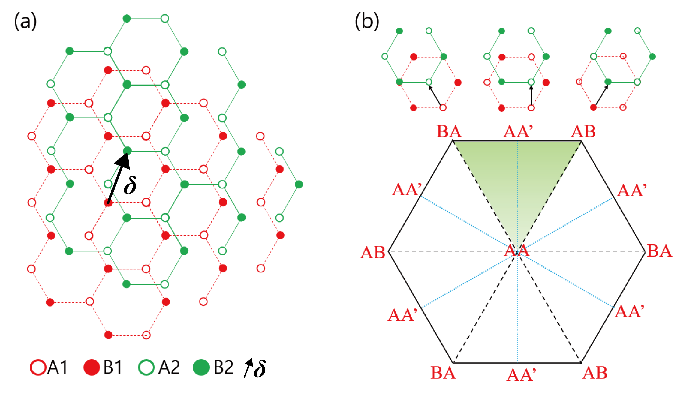
In order to consider the effects of finite translation in multilayer graphene band structure we begin by the simplest example of bilayer graphene where the position of the top layer with respect to the bottom layer is represented by a translation vector , as shown in Fig. 1(a). If we set for the AA stacking structure, then correspond to the AB and BA stacking structures, respectively, while corresponds to AA′ stacking structure (Park et al., 2015), where Å is the lattice constant. Due to the periodic structure of bilayer graphene, the layer translation vector space can be divided into triangular irreducible zones, as shown in Fig. 1(b) with several representative stacking structures. Similarly, we can easily generalize from the bilayer graphene to multilayer cases. For multilayer graphene, we assume for simplicity that each layer is translated along the same direction and the relative translations between the adjacent layers are the same.
The electronic band structure of multilayer graphene nanoribbon (MGNR) geometries with one-dimensional band dispersions offers a convenient platform for representing the dispersion of the ZLMs. To describe band structures of the layer translated MGNRs, we use a tight-binding method taking into account remote hopping terms up to the 15 nearest-neighbor unit cells to fully account for contributions from all arbitrarily displaced atoms and at the same time to evolve the Hamiltonian smoothly with the layer translation.
The Hamiltonian in the second-quantized form reads
| (1) | |||||
where () corresponds to the creation (annihilation) operator for an electron on the -th site in the -th layer. The first term represents the single-layer graphene Hamiltonian for the -th layer with on-site potential energy and intralayer hopping for each -th layer. The second term describes the interlayer coupling between the -th layer and -th layer with interlayer tunneling . Note that the index represents only the site of each atom since spin does not play any role in our demonstration. As an approximation we consider the interlayer hopping terms only between adjacent layers. To fully account for contribution between arbitrarily displaced atoms, we include remote hopping terms beyond the nearest-neighbor approximation with the exponentially decaying form with distance,
| (2) |
where eV and eV represent the nearest-neighbor intralayer and interlayer hopping terms at the distance and , respectively, where Å is the in-plane carbon-carbon distance and Å is the interlayer separation. Here is a displacement vector between two carbon atoms and is the angle between the axis and . Following Ref. Koshino, 2013, we take Å.
The valley Chern number associated with each gapped Dirac cone, defined as the Chern number for a single valley, allows us to count the number of expected ZLMs in the presence of a domain wall. For example, for rhombohedral stacked -layer graphene, the valley Chern number can be easily estimated from the low energy effective theory given by
| (3) |
where with and Min and MacDonald (2008a, b). The corresponding valley Chern number is given by , where is the valley index and represents the direction of rhombohedral stacking. [For example, in bilayer graphene corresponds to AB (BA) stacking.] Note that the valley Chern number is proportional to the valley index and the sign of , and its sign is flipped if we reverse the stacking sequence. Thus the valley Chern numbers change across the interface between two domains with opposite or . Although the validity of this effective model is limited to low energies near the Fermi energy, it is useful for illustrating the topological nature of the valley Chern number in rhombohedral -layer graphene that should lead to gapless metallic states in each valley in the presence of domain walls with opposite stacking order or perpendicular electric field direction.
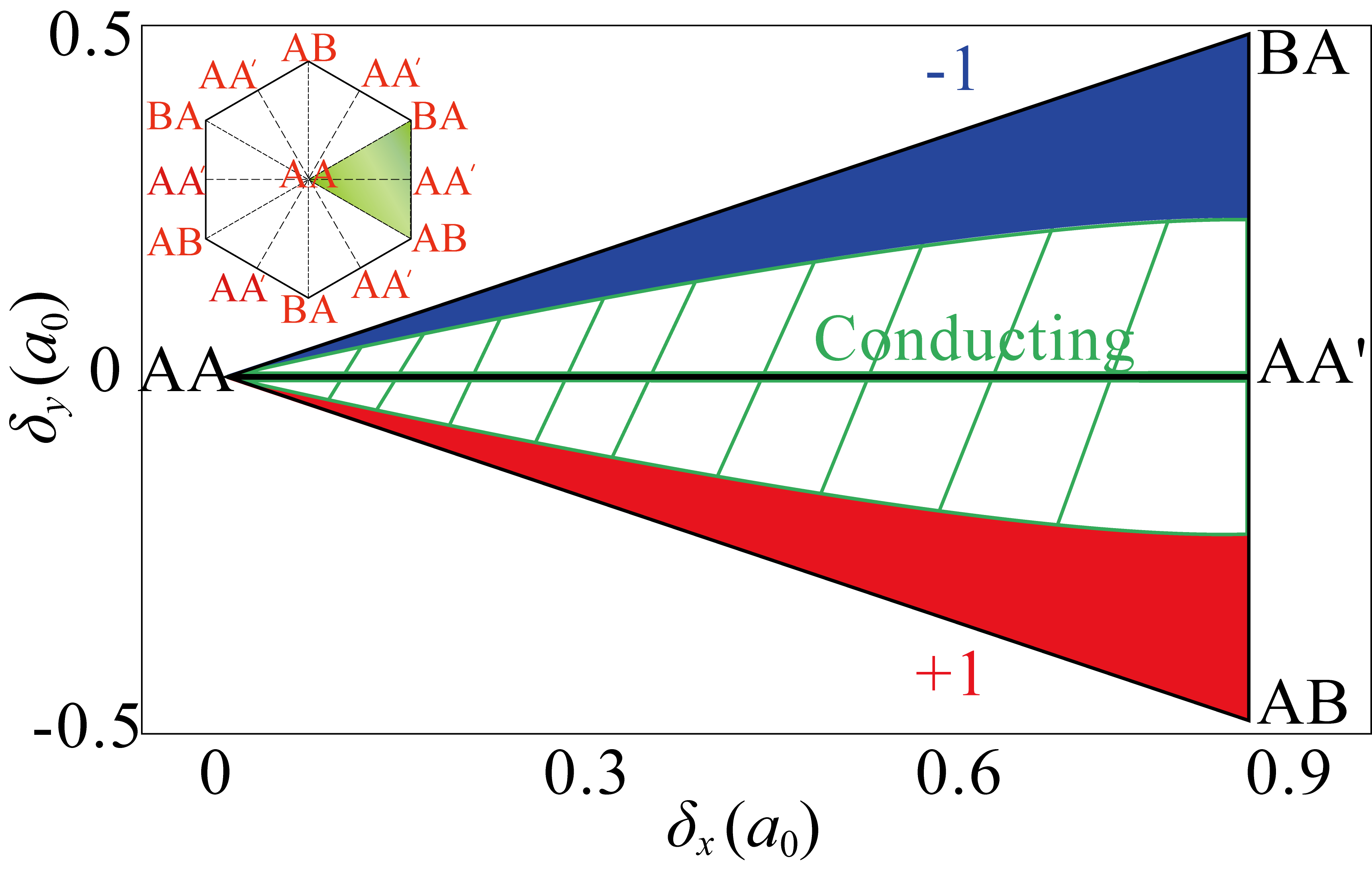
When we introduce an in-plane translation in a gapped phase we expect that the valley Chern number, which characterizes the topological property of the band structure in the continuum limit around a valley, will remain unchanged until the energy bands near the Fermi level touch each other. Our explicit calculation of the Chern number through integration of the Berry curvature around each valley confirms that indeed this is the case, as we illustrate in the Chern number phase space map in Fig. 2 for which we use a constant interlayer potential difference eV. The distinct insulating regions represented in Fig. 2 in red (blue) with the valley Chern numbers () at the K valley have dominantly AB (BA) stacking and are divided by the line connecting the AA and AA′ stacking configurations. The system remains invariably metallic at this division line even if the phase map changes depending on the magnitude of . We will show that the ZLMs appear even in stacking faulted systems whenever there are two insulating domains with opposite Chern numbers, resulting either from opposing stacking regions (AB/BA-like) or electric field directions.
III zero-line Modes between stacking faulted domains
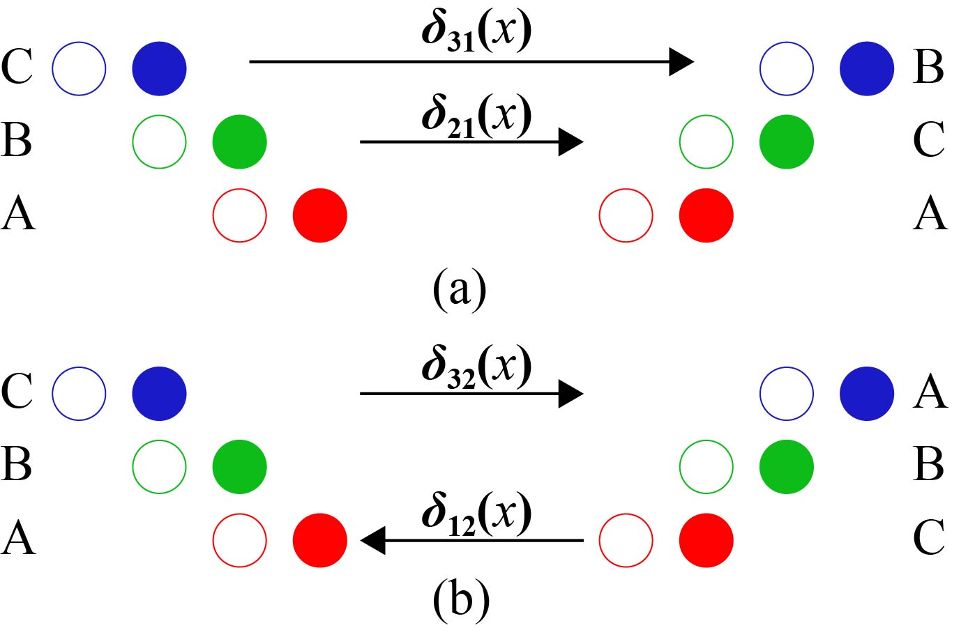
We study the impact of the stacking faults in the ZLMs by analyzing their real-space probability distribution and the energy band structure. The first case to consider is the layer stacking domain wall (LSDW) (Zhang et al., 2013) in a bilayer graphene nanoribbon (2GNR) under the influence of a constant interlayer potential difference. Figure 3 schematically illustrates a 2GNR with a LSDW constructed by sliding the carbon atoms continuously as
| (4) |
where and are layer translation vectors in domains 1 and 2, respectively and is distance from the starting point of the domain wall. The domain wall size is chosen to be about 10 nm to meet the observed domain wall length Butz et al. (2014); Ju et al. (2015); Lin et al. (2013), and the size of each domain is set as 136 nm in our calculation. A different choice of displacement vector field , for example, a variation along the displacement direction, does not change the result qualitatively. The effect of the domain wall size will be discussed later.
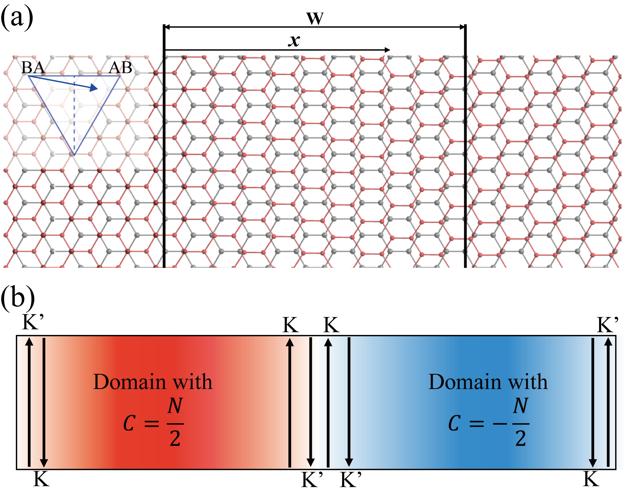
The 2GNR in Fig. 3 has a finite width along the horizontal axis and extends infinitely along the vertical direction, which allows us to use periodic boundary condition with a well-defined crystal momentum . In the middle of the ribbon, there is a domain wall of width where the stacking structure changes smoothly from BA to AB stacking. The arrow in the inset is the trace of the head of displacement vector field showing how stacking changes across the domain wall from the left to right domains.
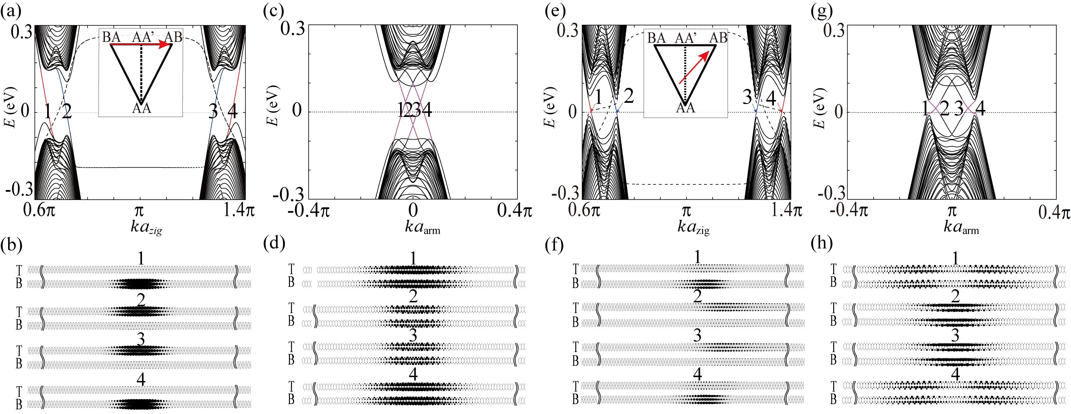
When we carry out explicit tight-binding calculations in the ribbon geometries, we can observe that the ZLMs are indeed present even when the stacking configurations at the domains have an in-plane shift. In Fig. 4 we show the band structures of 2GNRs with LSDW and the corresponding probability distribution for states slightly above the Fermi level for zigzag and armchair edge alignments. The left two panels are for LSDW with AB and BA stacked domains at the two sides whereas the right two panels are for LSDW with two domains which have layer-translated stacking arrangements whose translation vectors are separated by the AA-AA′ line, as seen in the insets of Figs. 4(a) and 4(e), respectively. First consider the AB-BA nanoribbon with the zigzag arrangement in Figs. 4(a) and 4(b). The dashed lines in Fig. 4(a) represent the edge state energy bands whose zero-energy states are localized mainly on the outer edges Castro et al. (2008); Jung et al. (2011); Li et al. (2012); Delplace et al. (2011).The red and blue solid lines represent the energy bands whose zero-energy states are localized around the domain wall, as seen by the size of black filled circles in Fig. 4(b). (Here we omitted the edge states in the probability distributions because we focus on the ZLMs.) Note that there are two dispersive ZLMs per valley, which can be estimated by the valley Chern number difference between the two sides, as shown in previous works (Ju et al., 2015; Vaezi et al., 2013; Zhang et al., 2013; Jung et al., 2011). Importantly, these ZLMs still appear when the domains of 2GNR are not in Bernal stacking as seen in Figs. 4(e) and 4(f). Note that the probability distribution of the modes 3 and 4 are identical to the modes 2 and 1, respectively, due to time-reversal symmetry. A similar conclusion can be reached to armchair nanoribbons as seen in Figs. 4(c), 4(d), 4(g), and 4(h), in which edge states are absent. For the armchair nanoribbons, however, the K and K’ valleys overlap in momentum space and the ZLMs anticross leaving a small gap due to the mixing of the two valleys. Our calculations support the fact that the presence of ZLMs are mainly defined by the difference in the valley Chern numbers between the left and right domains in the nanoribbon geometry studied.
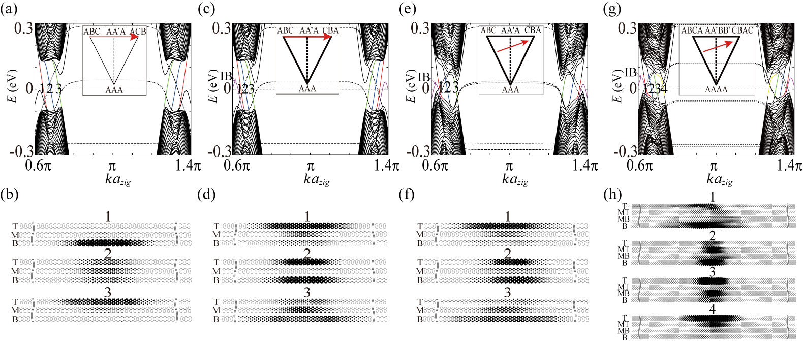
For multilayers beyond bilayer graphene such as a trilayer, the analysis becomes more complicated due to the diverse options for choosing a fixed layer when creating a LSDW. For example, for trilayer graphene nanoribbons (3GNRs), we can either fix the bottom layer while moving the middle and top layers in the same direction or fix the middle layer while moving the top and bottom layers in the opposite direction. (As assumed in Sec. II, we will not consider the case with staggered layer translation.) We distinguish these two options by naming ABC-ACB and ABC-CBA, respectively, as seen in Fig. 5. Here represents the displacements of atoms in the -th layer relative to the atoms in the -th layer. For the ABC-ACB type LSDW, atoms in each layer are displaced in accordance with , while the relation between two displacement vector fields is for the ABC-CBA type LSDW. We further assume that for simplicity the interlayer potential difference is the same along the layers.
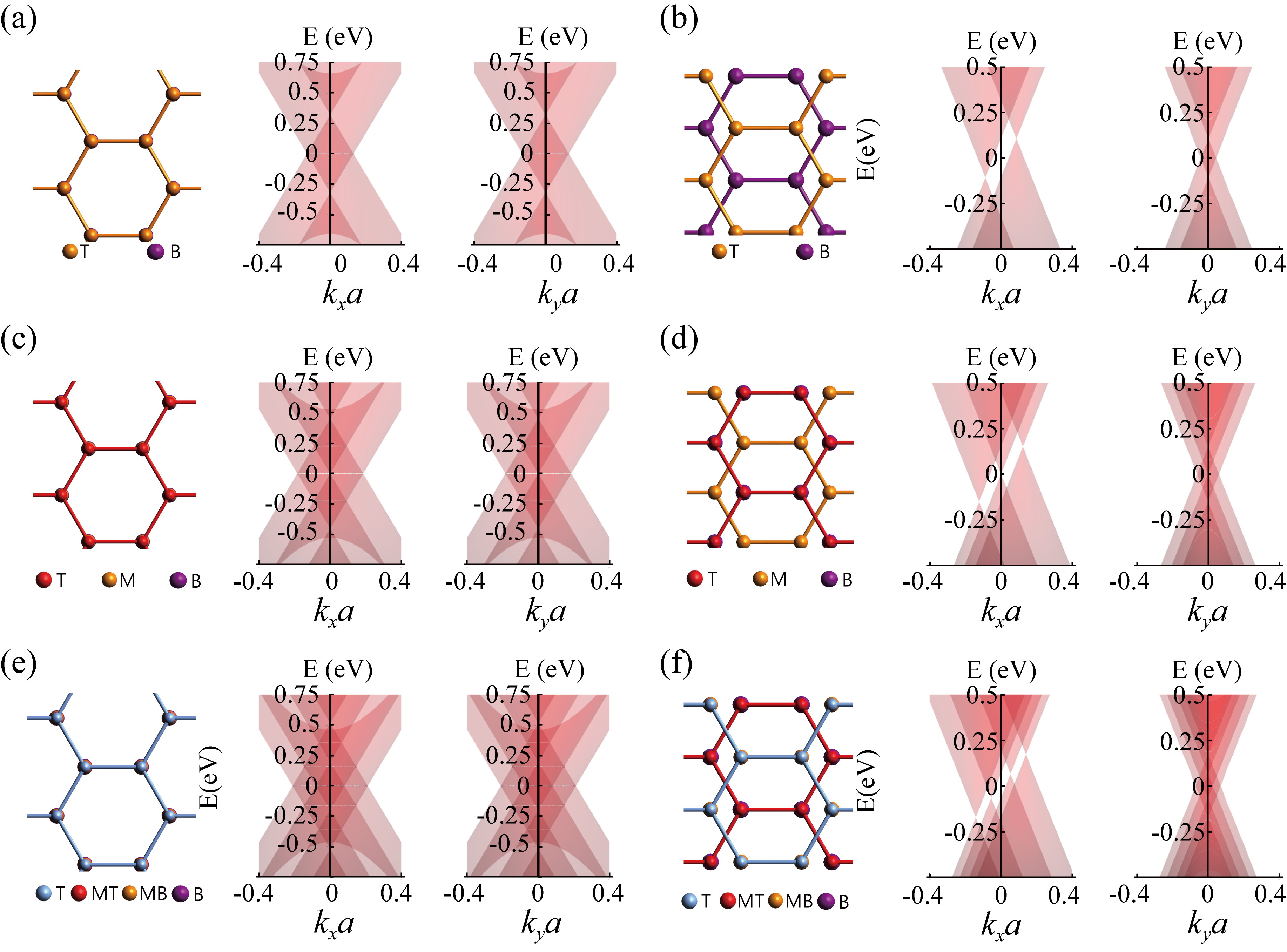
Figure 6 shows electronic band structures of 3GNRs and 4GNRs with LSDW and their probability distributions for ZLMs. Similarly to 2GNRs with LSDW, the ZLMs appear not only in ABC-ACB or ABC-CBA type translation but also in the deviated translations as long as the translations in the two domains remain in the opposite sides separated by AAA-AA′A line in layer translation vector space. (For the band structure of AAA and AA′A, see Appendix B.) Both zigzag and armchair arrangements show results similar to those for 2GNR-LSDW. Note that the purple lines in Figs. 6(c) and 6(e) are the interface bound modes (Bi et al., 2015; Zarenia et al., 2011; Qiao et al., 2011). These interface bound modes also have probability distributions localized around the domain wall. However, their energy-momentum dispersion depends more strongly on the geometry of the interface and electric field profile than the energy-momentum dispersion of ZLMs does (Qiao et al., 2011). Moreover, they fade away into the bulk energy levels when a sufficiently large electric field is applied while the ZLMs survive robustly maintaining its gapless dispersion.
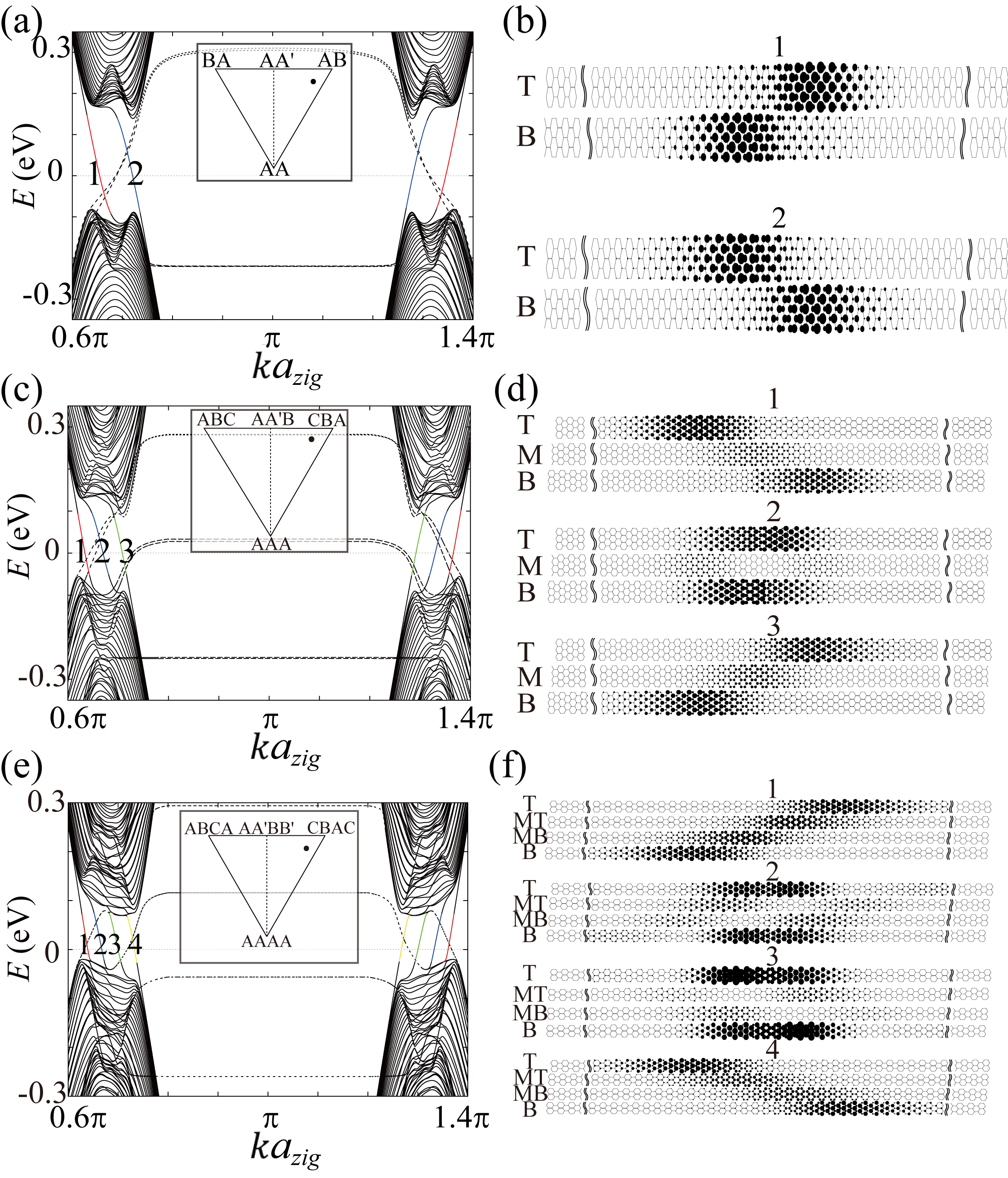
The conclusions that we can draw from our calculations of the LSDW configurations apply equally for ZLMs that occur in the domain wall between domains where anti-parallel electric fields are applied. Reversing the direction of perpendicular electric fields changes the sign of the valley Chern number, which can be seen in the effective model in Eq. (3). Therefore, like MGNRs with LSDW, there would be metallic states at the interface between two domains which have the same stacking structure but opposite field directions. We call this type of domain wall electric field domain wall (EFDW). Similarly as LSDW, we construct the EFDW by changing the potential configuration linearly across the domain wall as
| (5) |
with the domain wall size . Here we choose the sharp domain wall with with abrupt change of the field direction to minimize the number of unwanted interface bound modes Zarenia et al. (2011). The effect of the domain wall size on ZLMs will be discussed in Sec. IV.
For Bernal-stacked 2GNRs with EFDW, the properties of the metallic states have been studied previously in several papers (Zhang et al., 2013; Jung et al., 2011; Martin et al., 2008). Here we consider a more generalized setup consisting of stacking faulted domains due to in-plane layer translation rather than a perfect rhombohedral stacking, as shown in Fig. 7 for various MGNRs. In agreement with prior calculations, we can observe that the number of metallic states in each valley is always equal to the number of layer , as expected from Eq. (3) for the effective model which describes a chiral two-dimensional electron gas with chirality index .
IV Band gap opening in stacking faulted domains and width of the zero-line Modes
For practical application of ZLMs in valleytronics devices, it is required to estimate the proper electric field strength and size of domain wall for the observation of ZLMs. In this section, we present numerical results for the electric field strength required to open an energy gap in stacking faulted domains and the domain wall size dependence of the ZLM widths. The band gap opening that accompanies the application of a perpendicular electric field in rhombohedral graphene is a necessary condition to create the gapped domains flanking the ZLMs. It was shown that the ability of a perpendicular electric field to open up a band gap in bilayer graphene will persist for small departures from the ideal Bernal stacking (Park et al., 2015). This is true provided that the applied electric field is large enough to overcome the band asymmetries introduced around the K points due to the stacking fault. Here we present a more detailed account on the relationship between the required critical perpendicular electric field for the onset of a band gap in the presence of a stacking fault. Figure 8 shows a typical example of the onset of band gap opening in layer translated multilayer graphene where each band structure represents gradually increasing interlayer potential differences. When the effective potential between the layers is zero, this layer-translated bilayer graphene has a metallic band structure with valley degenerate electron and hole pockets in the Brillouin zone. When the interlayer potential difference is increased, the bands containing electron (hole) pockets are raised (lowered) in energy accordingly. When the effective potential reaches a critical value , the electron and hole pockets disappear completely and the bilayer graphene becomes an insulator from this point onwards.
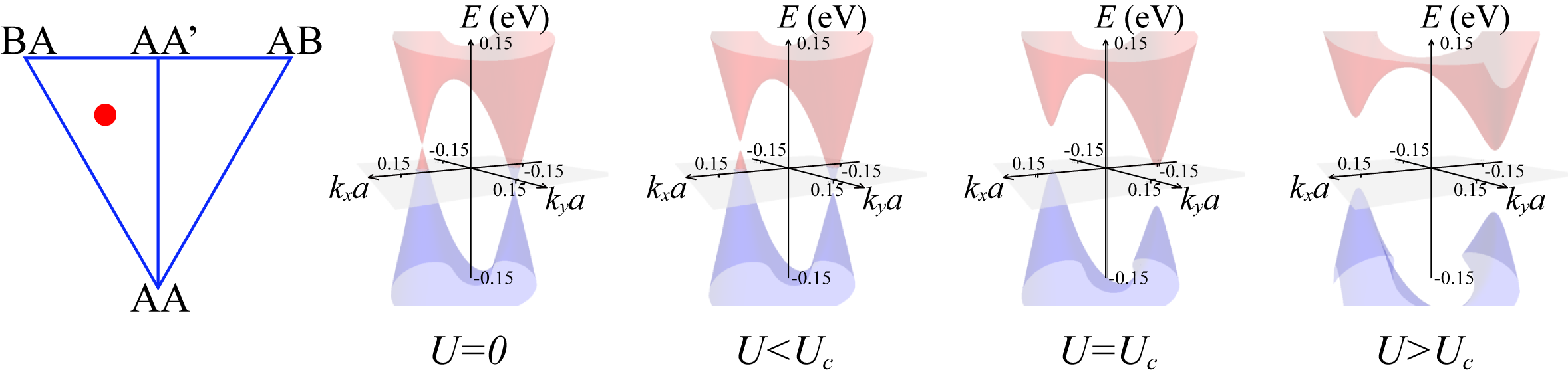
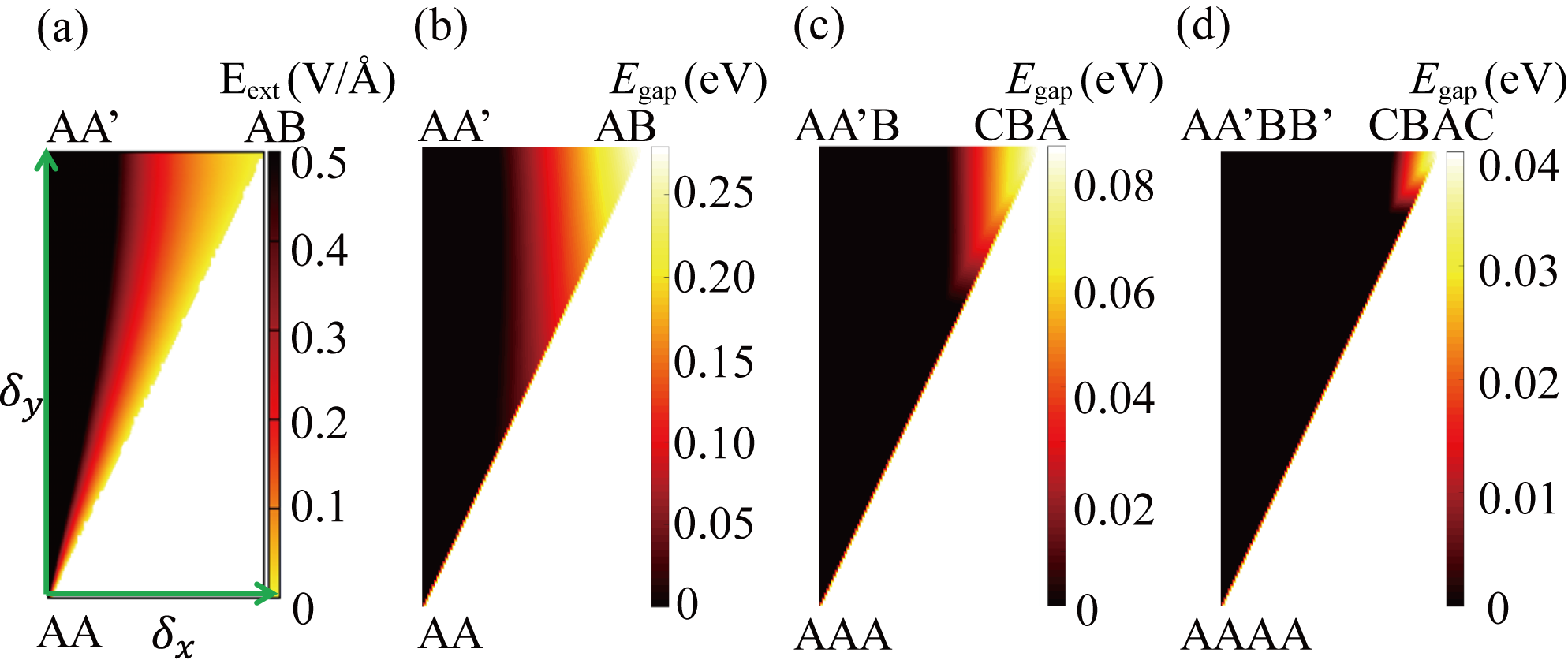
It is experimentally important to know the critical electric field required for opening a gap in order to trigger an insulating phase. Figure 9(a) shows the critical external electric field strength for layer-translated bulk bilayer graphene obtained from a self-consistent Hartree method Min et al. (2007) using a tight-binding model of Eq. (1). We obtained an analytic expression in Eq. (10) for the critical field required for opening a band gap in bilayer graphene by solving the roots of the fourth order polynomial equation of the four-band effective Hamiltonian. Along the AA-AA′ stacking line the critical field becomes infinite indicating that any stacking along the AA-AA′ line remains always metallic. Note that the topologically distinct domains characterized by the valley Chern numbers are separated by this AA and AA′ line, as seen in Fig. 4.
The magnitude of the achievable gap depends on the particular stacking configuration. In Figs. 9(b)(d) we show the band gaps that develop under an external electric field of as a function of layer translation, in which we clearly see a decrease in the gap size as we move closer to the AA-AA′ line for bilayer graphene (AAA-AA′A line for trilayer graphene, AAAA-AA′AA′ line for tetralayer graphene). As discussed earlier, this gap decrease has its origin in the band structure of the layer-translated multilayer graphene. By means of a self-consistent Hartree screening calculation, we verified that the effective potential difference between layers under electric fields is almost independent of stacking configuration in bilayer graphene. For example, the potential difference between layers in bilayer graphene under electric fields of 0.5 turns out to be about 0.63 eV for all layer translated stackings. This result partially justifies the validity of our assumption of constant effective interlayer potentials in our calculation for MGNR-LSDW, though the stacking dependence of the interlayer potentials becomes more important as the number of layers increases.
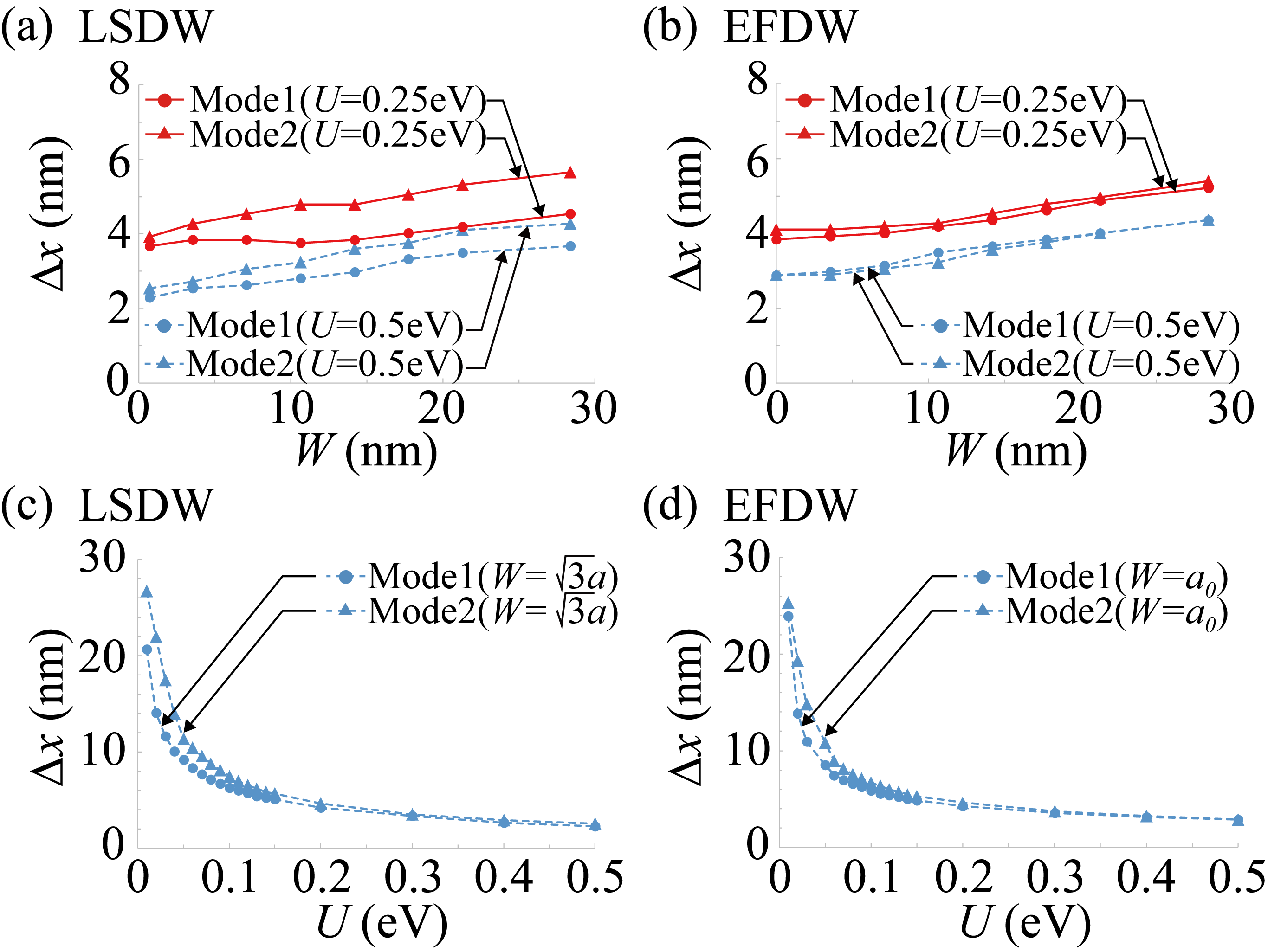
In order to provide a practical guidance for experiments aiming to probe ZLM local density of states, we analyzed the influence of the domain wall size and the magnitude of the potential difference on the width of ZLM defined as the distance that contains 90% of probability distribution centered inside the domain wall. In Figs. 10(a) and 10(b), the ZLM width versus the domain wall width is illustrated for LSDW and EFDW, respectively, for the potential difference eV and eV. We find that even in the sharp domain wall () the ZLMs have a finite size, and the size increases relatively weakly as the domain wall width increases. Figures 10(c) and 10(d) show the potential strength dependence of the ZLM size for LSDW and EFDW, respectively, with and . In general, the width of ZLMs decreases rapidly as the potential difference increases for both LSDW and EFDW.
V Summary and conclusion
In this work we have studied the zero-line modes (ZLMs) in multilayer graphene nanoribbon geometries in the presence of domains whose interlayer stacking deviates from perfect chiral stacking, namely the Bernal alignment for bilayer and rhombohedral stacking for multilayers, providing a systematic and comprehensive picture on the existence of ZLMs in arbitrarily displaced multilayer graphene. The analysis carried out in this work expands the validity of the analysis of the ZLMs based on the valley Hall conductivity of the insulating domains for chirally stacked multilayer graphene and confirms the possibility of realizing the ZLMs in actual experimental devices where stacking faults may be present either due to unwanted disorder effects or artificial strain fields. We have discussed the conditions of stacking order in the bulk and external perpendicular electric fields required for opening the band gap in the bulk necessary to generate the ZLMs in the system. We can conclude that stacking faulted domains that deviate from perfect rhombohedral stacking can also host ZLMs provided that sufficiently large perpendicular electric fields can be applied to open up a band gap in the bulk. The valley Chern number signs for the bulk are defined by stacking configurations that can be classified as AB-like and BA-like regions and are divided by the AA-AA′ stacking lines. We found that a larger electric field is required to open up a band gap when the perfect chiral stacking is modified through in-plane sliding. This critical field has been obtained both analytically and numerically for a variety of stacking configurations. The explicit calculations of the ZLM probability distribution for both layer stacking and electric field domain walls with zigzag and armchair edge alignments provide information that can be useful when designing junctions made of intersecting ZLMs whose current partitioning properties are expected to depend on the overlap between the incoming and outgoing modes (Qiao et al., 2014; Ezawa, 2013). Our work also provides insight for understanding the ZLMs that can be expected in layer misaligned systems such as twisted bilayer graphene and multilayers with tilted boundaries where spatially varying local stacking configurations are present.
Acknowledgements.
This research was supported by Basic Science Research Program through the National Research Foundation of Korea (NRF) funded by the Ministry of Education (MOE) of Korea under Grant No. 2015R1D1A1A01058071. G.K. thanks the financial support from the Priority Research Center Program (2010-0020207), and the Basic Science Research Program (2013R1A2009131) through NRF funded by the MOE. J.J. acknowledges financial support from the Korean NRF through the grant NRF-2016R1A2B4010105.Appendix A Critical potential difference in layer-translated bilayer graphene
The Hamiltonian for bilayer graphene with arbitrary layer translation in a continuum model can be written as(Koshino, 2013)
| (6) |
where and interlayer hopping terms are given by
| (7) | ||||
| (8) | ||||
| (9) |
where for K, K′ valleys and is the layer translation vector defined in Fig. 1 with for AA stacking. The above expression for interlayer hopping terms is obtained through Fourier transformation at the corner of the first Brillouin zoneKoshino (2013) and resembles the stacking-dependent interlayer interaction in bilayer graphene given in Ref. Jung et al., 2014. Then the required effective potential to open energy gap can be obtained as
| (10) |
Note that stackings along AA-AA′ line corresponding to require an infinite potential difference for gap opening. This means that bilayer graphene in theses stackings can not be insulators by applying a perpendicular electric field within the continuum model approximation. However, when two Dirac cones at the K and K’ valleys are directed toward the M point and meet each other, it is possible that stacking along AA-AA’ line can be gapped even at a large but finite potential energy difference.
Appendix B Energy dispersions in various layer-translated multilayer graphene
In this appendix, we illustrate various atomic structures and corresponding energy dispersions for the layer-translated multilayer graphene configurations labeled as AA, AA′, AAA, AAAA, AA′A and AA′AA′ and discussed in the main text.
References
- Martin et al. (2008) I. Martin, Y. M. Blanter, and A. F. Morpurgo, Phys. Rev. Lett. 100, 036804 (2008).
- Jung et al. (2011) J. Jung, F. Zhang, Z. Qiao, and A. H. MacDonald, Phys. Rev. B 84, 075418 (2011).
- Bi et al. (2015) X. Bi, J. Jung, and Z. Qiao, Phys. Rev. B 92, 235421 (2015).
- Zhang et al. (2013) F. Zhang, A. H. MacDonald, and E. J. Mele, Proc. Natl. Acad. Sci. USA. 110, 10546 (2013).
- de Sena et al. (2014) S. H. R. de Sena, J. M. Pereira, F. M. Peeters, and G. a. Farias, Phys. Rev. B 89, 035420 (2014).
- Semenoff et al. (2008) G. W. Semenoff, V. Semenoff, and F. Zhou, Phys. Rev. Lett. 101, 087204 (2008).
- Vaezi et al. (2013) A. Vaezi, Y. Liang, D. H. Ngai, L. Yang, and E.-A. Kim, Phys. Rev. X 3, 021018 (2013).
- Jung et al. (2012) J. Jung, Z. Qiao, Q. Niu, and A. H. MacDonald, Nano Lett. 12, 2936 (2012).
- Volovik (2003) G. E. Volovik, The Universe in a Helium Droplet (Oxford University Press, 2003).
- Yao et al. (2009) W. Yao, S. a. Yang, and Q. Niu, Phys. Rev. Lett. 102, 096801 (2009).
- Xiao et al. (2007) D. Xiao, W. Yao, and Q. Niu, Phys. Rev. Lett. 99, 236809 (2007).
- Killi et al. (2012) M. Killi, S. Wu, and A. Paramekanti, Int. J. Mod. Phys. B 26, 1242007 (2012).
- Qiao et al. (2011) Z. Qiao, J. Jung, Q. Niu, and A. H. MacDonald, Nano Lett. 11, 3453 (2011).
- Qiao et al. (2014) Z. Qiao, J. Jung, C. Lin, Y. Ren, A. H. MacDonald, and Q. Niu, Phys. Rev. Lett. 112, 206601 (2014).
- Schroer et al. (2015) A. Schroer, P. G. Silvestrov, and P. Recher, Phys. Rev. B 92, 241404 (2015).
- Alden et al. (2013) J. S. Alden, A. W. Tsen, P. Y. Huang, R. Hovden, L. Brown, J. Park, D. A. Muller, and P. L. McEuen, Proc. Natl. Acad. Sci. USA. 110, 11256 (2013).
- Ju et al. (2015) L. Ju, Z. Shi, N. Nair, Y. Lv, C. Jin, J. Velasco, C. Ojeda-Aristizabal, H. A. Bechtel, M. C. Martin, A. Zettl, J. Analytis, and F. Wang, Nature 520, 650 (2015).
- Li et al. (2016) J. Li, K. Wang, K. J. McFaul, Z. Zern, Y. F. Ren, K. Watanabe, T. Taniguchi, Z. H. Qiao, and J. Zhu, Nat. Nanotechnol. (2016), 10.1038/nnano.2016.158.
- Jung et al. (2014) J. Jung, A. Raoux, Z. Qiao, and A. H. MacDonald, Phys. Rev. B 89, 205414 (2014).
- Park et al. (2015) C. Park, J. Ryou, S. Hong, B. G. Sumpter, G. Kim, and M. Yoon, Phys. Rev. Lett. 115, 015502 (2015).
- Koshino (2013) M. Koshino, Phys. Rev. B 88, 115409 (2013).
- Min and MacDonald (2008a) H. Min and A. H. MacDonald, Prog. Theor. Phys. Suppl. 176, 227 (2008a).
- Min and MacDonald (2008b) H. Min and A. H. MacDonald, Phys. Rev. B 77, 155416 (2008b).
- Butz et al. (2014) B. Butz, C. Dolle, F. Niekiel, K. Weber, D. Waldmann, H. B. Weber, B. Meyer, and E. Spiecker, Nature 505, 533 (2014).
- Lin et al. (2013) J. Lin, W. Fang, W. Zhou, A. R. Lupini, J. C. Idrobo, J. Kong, S. J. Pennycook, and S. T. Pantelides, Nano Lett. 13, 3262 (2013).
- Castro et al. (2008) E. V. Castro, N. M. R. Peres, J. M. B. Lopes dos Santos, a. H. C. Neto, and F. Guinea, Phys. Rev. Lett. 100, 026802 (2008).
- Li et al. (2012) J. Li, I. Martin, M. Buttiker, and A. F. Morpurgo, Phys. Scr. 2012, 014021 (2012).
- Delplace et al. (2011) P. Delplace, D. Ullmo, and G. Montambaux, Phys. Rev. B 84, 195452 (2011).
- Zarenia et al. (2011) M. Zarenia, J. M. Pereira, G. A. Farias, and F. M. Peeters, Phys. Rev. B 84, 125451 (2011).
- Min et al. (2007) H. Min, B. Sahu, S. K. Banerjee, and A. H. MacDonald, Phys. Rev. B 75, 155115 (2007).
- Ezawa (2013) M. Ezawa, Phys. Rev. B 88, 161406 (2013).