Equivalent circuit representation of hysteresis in solar cells that considers interface charge accumulation: Potential cause of hysteresis in perovskite solar cells
Abstract
If charge carriers accumulate in the charge transport layer of a solar cell, then the transient response of the electric field that originates from these accumulated charges results in hysteresis in the current-voltage (-) characteristics. While this mechanism was previously known, a theoretical model to explain these - characteristics has not been considered to date. We derived an equivalent circuit from the proposed hysteresis mechanism. By solving the equivalent circuit model, we were able to reproduce some of the features of hysteresis in perovskite solar cells.
Recently, organic-inorganic hybrid-perovskite solar cells have attracted considerable research attention because of the rapid increase in the power conversion efficiency that can be gained by avoiding the use of electrolytes. Green and Snaith (2014) Perovskite solar cells can be fabricated using solution-based processes and low-cost materials, which gives them an advantage in the solar cell market. Green and Snaith (2014) The power conversion efficiency of these devices is more than % Meloni et al. (2016) and is approaching the theoretically estimated limit. Seki et al. (2015) At present, perovskite solar cells are considered to be neither junction-type solar cells nor excitonic-type solar cells like organic solar cells. The standard structure of a perovskite solar cell includes a charge transport layer, where holes or electrons are selectively transported to the appropriate electrode, thus suppressing recombination losses. Perovskite solar cells have unique features that are not found in conventional solar cells. However, unresolved issues remain with regard to their unique properties. One major issue for perovskite solar cells is the hysteresis that appears in their electrical characteristics. Snaith et al. (2014); Meloni et al. (2016); Tress et al. (2015); Unger et al. (2014); Zhang et al. (2015); Chen et al. (2016); Jena et al. (2016); Cojocaru et al. (2015); Ono et al. (2015); Nagaoka et al. (2015); Tao et al. (2015)
To aid in understanding of the electrical processes in a solar cell, the current density, , is studied by varying the applied voltage, . The maximum power conversion efficiencies (PCEs) of the devices can then be obtained from these - characteristics. In perovskite solar cells, hysteresis is often observed in the - characteristics. If hysteresis is present, then it becomes difficult to identify the maximum power point. Snaith et al. (2014); Zhang et al. (2015); Jena et al. (2016)
In attempts to determine the possible origin of the hysteresis behavior, several potential mechanisms have been proposed. Snaith et al. (2014); Zhang et al. (2015); Jena et al. (2016); Chen et al. (2016); Cojocaru et al. (2015); Ono et al. (2015); Meloni et al. (2016); Zhou et al. (2015); Nagaoka et al. (2015); Tao et al. (2015); Unger et al. (2014) Some experiments have shown that the hysteresis is correlated with the ferroelectric characteristics of the perovskite materials. Snaith et al. (2014); Zhang et al. (2015); Unger et al. (2014); Zhou et al. (2015) The internal electric field that is associated with the movement of cations or anions in the perovskite material is also considered to be related to the hysteresis. Snaith et al. (2014); Zhang et al. (2015); Meloni et al. (2016); Chen et al. (2016); Zhou et al. (2015) In this work, we consider a mechanism by the electric field from the accumulated charges in the charge transport layer. Chen et al. (2016); Jena et al. (2016); Cojocaru et al. (2015); Ono et al. (2015); Nagaoka et al. (2015); Tao et al. (2015) While this mechanism was previously known, a theoretical model to explain the - characteristics of the device has not previously been considered. This mechanism could also be applied in other situations where charge accumulation occurs within the charge generation layer. In this case, the accumulated charges at the interface can be ions.
In equivalent circuit models of solar cells, the dark current is generally represented using a diode equation that was given by Sze and Ng (2006): where , , and are the elementary charge, the reverse saturation current density and the applied voltage across the diode, respectively; is the Boltzmann constant, is the temperature, and is a phenomenological constant that is equal to one for an ideal diode. When there is a photo-generated current density, , the total current density in the circuit element is then given by Sze and Ng (2006)
| (1) |
where is the external voltage across the output terminal, and and represent the series and shunt resistances, respectively. The corresponding circuit is shown in Fig. 1 (a).
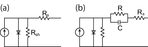
We consider the case where an additional resistor-capacitor (-) unit is inserted into the circuit, as shown in Fig. 1(b). The additional - circuit represents the voltage reduction that occurs through charge accumulation at the interfaces. The source of this voltage reduction may be the screening of the electric fields by the accumulated charges; this will be explained later in the paper. When the voltage applied to the - circuit, the external voltage across the output terminals, and the voltage across the element are denoted by , , and , respectively, these parameters are related by the following equation:
| (2) |
where the current density is given by
| (3) |
The current conservation law leads to
| (4) |
We then substitute Eqs. (2) and (3) into Eq. (4) to simulate the - curves by setting . In the steady state, the solution can be reduced to Eq. (1), with in the place of .
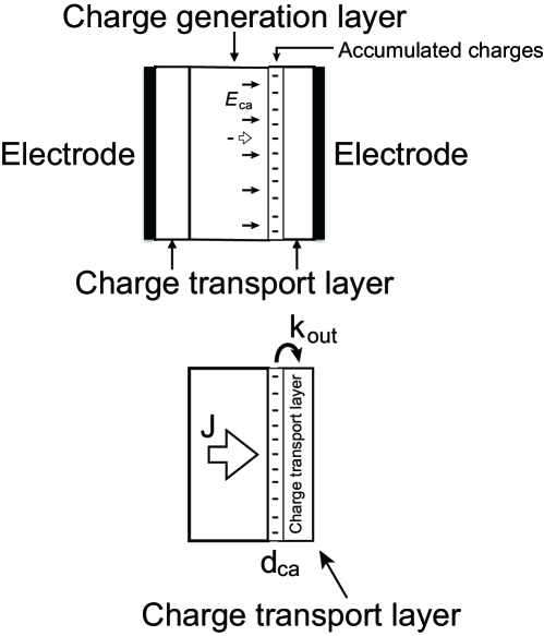
To provide a simple physical description, we consider the case where holes and electrons are generated in the charge generation layer and the carriers are transferred to each charge transport layer as shown in Fig. 2. Jena et al. (2016); Zhou et al. (2015) If these charge carriers accumulate at the interface between the charge generation layer and the charge transport layer on the right-hand side of the structure because the charge transfer rate to the charge transport layer is low, Jena et al. (2016); Zhou et al. (2015) the carrier density in the charge accumulation region, which is represented by , is given by the following rate equation:
| (5) |
where and represent the rate constant for charge carrier transfer from the charge accumulation region to the charge transport layer and the depth of the charge accumulation region, respectively. represents the current that flows out from the charge generation layer, as given by Eq. (3). is equal to the transmission coefficient of the current flow. If all the currents accumulate, we have . We consider the case where is smaller than the characteristic length of the concentration gradient, which means that the surface charge density can be given by . When the dielectric constants of the charge generation layer and the charge transport layer are denoted by and , respectively, the strength of the electric field from the accumulated charges is then given by using Gauss’s theorem. In Eq. (3), represents the voltage that is applied to the charge generation layer. The accumulated charges at the interface produce an electric field in the charge generation layer in a direction such that it opposes the carrier flow. Zhou et al. (2015) When a uniform electric field is applied to a charge generation layer of thickness in addition to the external voltage , then the net voltage that is applied to the charge generation layer is , where . By defining and , Eq. (5) can be reduced to Eq. (4), and the time constant that represents the transient response is given by . Therefore, we can conclude that the equivalent circuit model shown in Fig. 1, while approximate, represents the reduction of the electric field caused by charge accumulation at the interface between the charge generation layer and the charge transport layer.
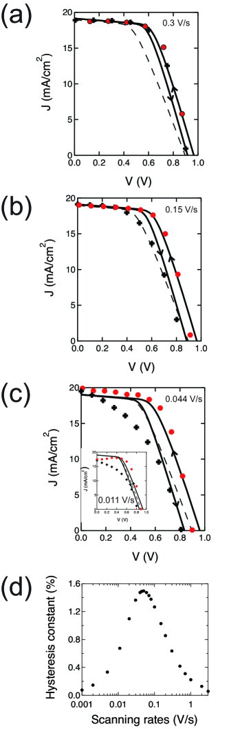
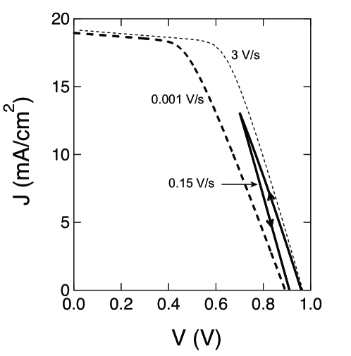
Figure 3 shows the current density as a function of the external applied voltage at various scan rates. We consider the situation where the applied voltage is maintained at 1.4 V for the first s, is then reduced to zero, and is reversed until the voltage returns to 1.4 V. The theoretical results are compared with the experimental results for planar heterojunction solar cells that are composed of layers of dense TiO2 (electron transport layer), perovskite and Spiro-OMeTAD (hole transport layer).Snaith et al. (2014) In the numerical calculations, we set K, mA/cm2, mA/cm2, cm2, cm2, F/ cm2, and cm2.
In the experiments, the hysteresis is higher when the voltage is scanned from open-circuit (OC) conditions than when initially scanned from the short-circuit (SC) conditions. Snaith et al. (2014); Zhang et al. (2015); Jena et al. (2016); Chen et al. (2016); Cojocaru et al. (2015); Ono et al. (2015); Meloni et al. (2016); Nagaoka et al. (2015); Unger et al. (2014); Liu et al. (2015); Kim and Park (2014) This trend was reproduced theoretically. The theoretical results also show that the hysteresis is greater on the OC side when compared with the SC side, as is commonly observed in planar cells. Tao et al. (2015); Nagaoka et al. (2015); Snaith et al. (2014); Zhang et al. (2015); Jena et al. (2016); Chen et al. (2016); Liu et al. (2015) (In supplemental figure S1, we show an improved comparison to experiment.)SI Recently, to reduce or even to eliminate this hysteresis, the TiO2 electron transport layer was replaced with another layer. *Tao15; Nagaoka et al. (2015); Shao et al. (2014); *Tripathi15 The results presented here are consistent with the reduced hysteresis that was obtained by introducing these structures, because the charges would accumulate at the interface between the charge generation layer and the electron transport layer.
The hysteresis was increased by reducing the scan rate from 0.3 to 0.044 V/s. When the scan rate was reduced further, the theoretical result shows a reduction in the hysteresis, but the hysteresis does not decrease in the experiment. The results are dependent on the experiments. In some experiments, the hysteresis was reduced, and the - curve then approaches the steady state result when the scan rate is low. Zhou et al. (2015); Tress et al. (2015) In Fig. 3(d), we show the hysteresis constant as a function of scan rate. The hysteresis constant was defined as the difference between the maximum PCEs for the different scan directions when assuming irradiation of mW cm-2. The hysteresis constants have a maximum as a function of the scan rate, and a similar maximum was recently reported. Zhou et al. (2015) The scan rate at the maximum is close to the inverse of the relaxation time given by s. If multiple relaxation times exist, the peak can then be broader and any reduction of the hysteresis produced by reducing the scan rate could hardly be observed.
The hysteresis was reduced by scanning the voltage at either an extremely slow speed or a high speed, as observed experimentally. Snaith et al. (2014); Zhang et al. (2015); Unger et al. (2014); Zhou et al. (2015); Chen et al. (2016); Tress et al. (2015) In Fig. 4, we show the results when the scan rate is extremely fast and when it is extremely slow. When the scan rate is low, the - curve approaches the steady state result. Unger et al. (2014); Zhou et al. (2015); Tress et al. (2015) At the opposite limit of the fast scan rate, the fill factor is high. The accumulated charge density is low at the OC side when compared with that at the SC side. When the voltage scan starts at the OC side and the scan rate is too fast for charge accumulation to occur, the current density reduction produced by the accumulated charges is suppressed.
In Fig. 4, we also show the results obtained when the voltage variation is small. Although the amplitude of the voltage variation is small, hysteresis was still obtained, as observed experimentally. Kim and Park (2014)
In our theory, is introduced to provide a simple physical description. The value of may be small. If we use , and assume that the relative dielectric constant is and nm, is then estimated to be sub-F/cm2 if . The reported values of were widely distributed, ranging from sub-F/cm2 to mF/cm2. Kim and Park (2014); Zarazua et al. (2016); *Bo15 These values and the high value of that was used to draw Fig. 3 suggest that only a proportion of the charge carriers are accumulated and that .
The hysteresis that occurs because of charge accumulation can be distinguished from that which occurs due to ferroelectric polarization reversal when the dielectric relaxation occurs sufficiently rapidly. If the ferroelectric polarization reversal occurs quickly, the hysteresis will then disappear using a small amplitude of the voltage scan. However, if the dielectric relaxation is slow, the induced surface charge in the dielectric causes hysteresis similar to that which occurs because of charge accumulation.
While our results are qualitative, they do clearly reproduce the basic hysteresis features, such as a higher current when scanned from the OC side as compared with that obtained when scanned from the SC side, and the large hysteresis at the OC side when compared with that on the SC side for the planar structured cells. Tao et al. (2015); Nagaoka et al. (2015); Snaith et al. (2014); Zhang et al. (2015); Jena et al. (2016); Chen et al. (2016)
Acknowledgements.
The author would like to thank Dr. Tetsuhiko Miyadera, Dr. Said Kazaoui, and Dr. Koji Matsubara at AIST for many fruitful discussions.References
- Green and Snaith (2014) M. A. Green and H. J. Snaith, Nat. Photon. 8, 506 (2014), and references cited therein.
- Meloni et al. (2016) S. Meloni, T. Moehl, W. Tress, M. Franckevičius, M. Saliba, Y. H. Lee, P. Gao, M. K. Nazeeruddin, S. M. Zakeeruddin, U. Rothlisberger, and M. Gätzel, Nat. Commun. 7, 10334 (2016).
- Seki et al. (2015) K. Seki, A. Furube, and Y. Yoshida, Jpn. J. Appl. Phys. 54, 08KF04 (2015).
- Snaith et al. (2014) H. J. Snaith, A. Abate, J. M. Ball, G. E. Eperon, T. Leijtens, N. K. Noel, S. D. Stranks, J. T.-W. Wang, K. Wojciechowski, and W. Zhang, J. Phys. Chem. Lett. 5, 1511 (2014).
- Tress et al. (2015) W. Tress, N. Marinova, T. Moehl, S. M. Zakeeruddin, M. K. Nazeeruddin, and M. Grätzel, Energy Environ. Sci. 8, 995 (2015).
- Unger et al. (2014) E. L. Unger, E. T. Hoke, C. D. Bailie, W. H. Nguyen, A. R. Bowring, T. Heumuller, M. G. Christoforo, and M. D. McGehee, Energy Environ. Sci. 7, 3690 (2014).
- Zhang et al. (2015) Y. Zhang, M. Liu, G. E. Eperon, T. C. Leijtens, D. McMeekin, M. Saliba, W. Zhang, M. de Bastiani, A. Petrozza, L. M. Herz, M. B. Johnston, H. Lin, and H. J. Snaith, Mater. Horiz. 2, 315 (2015).
- Chen et al. (2016) B. Chen, M. Yang, S. Priya, and K. Zhu, J. Phys. Chem. Lett. 7, 905 (2016).
- Jena et al. (2016) A. K. Jena, A. Kulkarni, M. Ikegami, and T. Miyasaka, J. Power Sources 309, 1 (2016).
- Cojocaru et al. (2015) L. Cojocaru, S. Uchida, P. V. V. Jayaweera, S. Kaneko, J. Nakazaki, T. Kubo, and H. Segawa, Chem. Lett. 44, 1750 (2015).
- Ono et al. (2015) L. K. Ono, S. R. Raga, S. Wang, Y. Kato, and Y. Qi, J. Mater. Chem. A 3, 9074 (2015).
- Nagaoka et al. (2015) H. Nagaoka, F. Ma, D. W. deQuilettes, S. M. Vorpahl, M. S. Glaz, A. E. Colbert, M. E. Ziffer, and D. S. Ginger, J. Phys. Chem. Lett. 6, 669 (2015).
- Tao et al. (2015) C. Tao, S. Neutzner, L. Colella, S. Marras, A. R. Srimath Kandada, M. Gandini, M. D. Bastiani, G. Pace, L. Manna, M. Caironi, C. Bertarelli, and A. Petrozza, Energy Environ. Sci. 8, 2365 (2015).
- Zhou et al. (2015) Y. Zhou, F. Huang, Y.-B. Cheng, and A. Gray-Weale, Phys. Chem. Chem. Phys. 17, 22604 (2015).
- Sze and Ng (2006) S. Sze and K. Ng, Physics of Semiconductor Devices (Wiley, 2006).
- Liu et al. (2015) C. Liu, J. Fan, X. Zhang, Y. Shen, L. Yang, and Y. Mai, ACS Appl. Mater. Interfaces 7, 9066 (2015).
- Kim and Park (2014) H.-S. Kim and N.-G. Park, J. Phys. Chem. Lett. 5, 2927 (2014).
- (18) See supplementary material at [URL will be inserted by AIP] for for an improved comparison to experiment.
- Shao et al. (2014) Y. Shao, Z. Xiao, C. Bi, Y. Yuan, and J. Huang, Nat Commun 5, 10.1038/ncomms6784 (2014).
- Tripathi et al. (2015) N. Tripathi, M. Yanagida, Y. Shirai, T. Masuda, L. Han, and K. Miyano, J. Mater. Chem. A 3, 12081 (2015).
- Zarazua et al. (2016) I. Zarazua, J. Bisquert, and G. Garcia-Belmonte, J. Phys. Chem. Lett. 7, 525 (2016).
- Wu et al. (2015) B. Wu, K. Fu, N. Yantara, G. Xing, S. Sun, T. C. Sum, and N. Mathews, Adv. Energy Mater. 5, 1500829 (2015).