Electrostatically confined monolayer graphene quantum dots with orbital and valley splittings
Abstract
The electrostatic confinement of massless charge carriers is hampered by Klein tunneling. Circumventing this problem in graphene mainly relies on carving out nanostructures or applying electric displacement fields to open a band gap in bilayer graphene. So far, these approaches suffer from edge disorder or insufficiently controlled localization of electrons. Here we realize an alternative strategy in monolayer graphene, by combining a homogeneous magnetic field and electrostatic confinement. Using the tip of a scanning tunneling microscope, we induce a confining potential in the Landau gaps of bulk graphene without the need for physical edges. Gating the localized states towards the Fermi energy leads to regular charging sequences with more than 40 Coulomb peaks exhibiting typical addition energies of -. Orbital splittings of - and a valley splitting of about 3 for the first orbital state can be deduced. These experimental observations are quantitatively reproduced by tight binding calculations, which include the interactions of the graphene with the aligned hexagonal boron nitride substrate. The demonstrated confinement approach appears suitable to create quantum dots with well-defined wave function properties beyond the reach of traditional techniques.
The charge carriers in graphene at low energies, described as massless Dirac quasiparticles 1, are expected to feature long spin coherence times 2, 3, 4, 5. Exploiting this property requires precise manipulation of individual Dirac electrons. Quantum dots (QDs) present an essential building block, yet providing tailored confinement in graphene has remained challenging. So far, e-beam lithography 6 and various other techniques 7, 8, 9, 10, 11, 12 have been used to design nanometer sized devices. However, their performance lacks behind, for example, GaAs QDs 13, 14, as disordered sample edges of patterned graphene result in uncontrolled charge localization and scattering 15, 6, 16, 17. So far, no clear evidence for fourfold degenerate charging sequences has been reported in transport measurements of tunable QDs. Moreover, failing to controllably lift graphene’s valley degeneracy renders spin qubits unfeasible 2, 18, 19.
Bilayer graphene could, in principle, improve the situation, since an electric displacement field opens a band gap at regular AB stacking 20. Indeed, electrostatically confined QDs in bilayer graphene exhibit Coulomb blockade 21, 22, 23, yet controlling the spin or valley degree of freedom of an individual state has also not been demonstrated. Moreover, confinement is still prone to parasitic conduction channels due to residual disorder in the band gap or conducting channels along domain walls of AB- and BA-stacked areas 24. Another approach exploits whispering gallery modes in electrostatically confined QDs 25, 26, 27, but here the control of the wave functions by gates is difficult and dwell times are extremely short (). On an even more intricate route, the tip of a scanning tunneling microscope (STM) is used to locally stretch a suspended monolayer graphene sheet 28. The onset of charge quantization due to induced strain showcases confinement by pseudomagnetic fields. Adding a real magnetic field leads to charging sequences with regular orbital but no valley splittings 28. Creating multiple QDs in this fashion would require independent strain control for every QD on the suspended graphene. Thus such an approach is barely scalable.
Landau quantization helps to overcome Klein tunneling by opening band gaps 21, 22, 23. An elegant method to exploit this by combining a magnetic field and an electrostatic potential has been proposed theoretically 29, 30, 31. Indeed, indications of such confinement have been found in metal contact induced pnp junctions 32, graphene on 33, 34 and a suspended graphene nano-ribbon 35. However, in these experiments the confinement potential was not tunable but was generated by electrostatic disorder.
Here, we demonstrate controlled confinement by a combination of magnetic and electrostatic fields. We use the tip-induced electrostatic potential of an STM 36, 37 in a field perpendicular to the graphene plane (Fig. 1a). Scanning tunneling spectroscopy (STS) reveals sequences of charging peaks by means of Coulomb staircases which appear when these confined states cross the Fermi energy . The peaks systematically group in quadruplets for electrons and holes corresponding to the fourfold (valley and spin) degeneracy in graphene (Fig. 1c,d). Moreover, some quadruplets separate into doublets due to an additional valley splitting induced by the hexagonal boron nitride (BN) substrate. STS as a function of reveals that the first confined states emerge from Landau levels (LLs) with indices . A third-nearest neighbor tight binding (TB) calculation 38, 39 reproduces the onset of charging events as function of tip voltage and , and the magnitude of orbital and valley splittings.
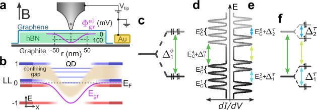
We now sketch the principle of our experiment. A homogeneous, perpendicular field condenses the electronic states of graphene into LLs at energies
| (1) |
where is the Fermi velocity and is the LL index 1. Consequently, energy gaps between the LLs emerge in the electronic spectrum. The smooth electrostatic potential (magenta line in Fig. 1a) induced by the STM tip locally shifts the eigenenergies of charge carriers relative to the bulk LL energy (eq 1). Shifting into the Landau gaps creates confined states (Fig. 1b) 30. The shape of determines the single-particle orbitals and energy levels, as in the case of artificial atoms 14. Orbital splittings separate the energy levels (Fig. 1c), which we deduce experimentally to be (see below) and, thus, is small compared to the first LL gap at . While pristine graphene exhibits a fourfold degeneracy, varying stacking orders of graphene on top of BN induce an additional valley splitting , which turns out to be smaller than in our experiment. The finite field creates a small Zeeman splitting estimated as at (-factor of 2, : Bohr’s magneton). Accordingly, the orbital splittings separate quadruplets of near-degenerate QD states, which exhibit a subtle spin-valley substructure (Fig. 1f).
We use the STM tip not only as source of the electrostatic potential and thus as gate for the QD states but also to sequence the energy level spectrum of the QD as the states cross , that is, as the charge on the QD changes by . This leads to a step in the tunneling current and a corresponding charging peak in the differential conductance . In addition to the single particle energy spacings, every additional electron on the dot needs to overcome the electrostatic repulsion to the electrons already inside the QD 40, given by the charging energy . Thus, we probe the total energetic separation of charge states and , given by the addition energy , where consists of , and/or . As we experimentally find (nearly independent of the charge state , see below), the quadruplet near-degeneracy of the QD states translates to quadruplet ordering of the charging peaks (Fig. 1d). Whenever either or significantly exceeds the other and temperature, quadruplets separate into doublets (Fig. 1e).
We prepare our sample (see Fig. 1a and Supplement) by dry-transferring 41, 42 a graphene flake onto BN 43, 44, 45. During this step we align both crystal lattices with a precision better than one degree (Supplement). Then we place this graphene/BN stack on a large graphite flake to avoid insulating areas and simplify navigating the STM tip. Any disorder potential present in the sample will limit the confinement as long as it is larger than the Landau level gaps, thus larger gaps (e.g., the LL0 - LL±1 gap) result in improved confinement. Moreover, the induced band bending will only be well-defined if the disorder potential is smaller than the maximum of . By using the dry-transfer technique 41, 42 and a graphite/BN substrate we reduce disorder in the graphene significantly 46, 47, 48.
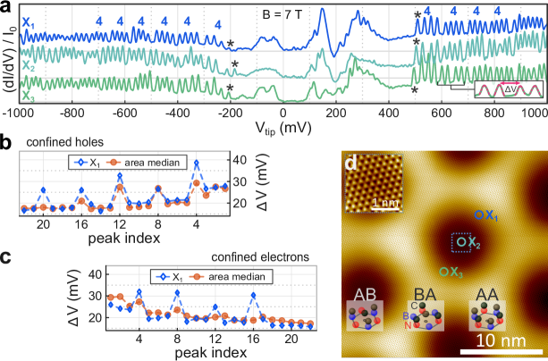
Probing the sample in our custom-build UHV-STM system 49 at K, we observe the superstructure with periodicity, which develops due to the small lattice mismatch of between graphene and BN 47. An atomically resolved STM image of this superstructure is presented in Figure 2d. Prior to measuring spectra, the tip-sample distance is adjusted at the stabilization voltage and current and then the feedback loop is turned off (Supplement). Figure 2a shows exemplary spectra, acquired at and adjusted to same vertical scale by dividing by the first value of the respective curve (Supplement). We observe pronounced, regularly spaced peaks for and . A closer look at the sequences reveals the expected grouping in quadruplets, which can still be distinguished up to the peak. This grouping becomes even more evident by directly comparing the voltage difference between adjacent peaks in Figure 2b,c: between quadruplets is up to twice as large as within the quadruplets indicating while and are significantly smaller. To further elucidate grouping patterns, we measure 6400 spectra at equidistant positions within a area, thus probing all areas of the superstructure. The median values (orange circles in Fig. 2b,c) portray the robust ordering into quadruplets on the hole side, implying generally dominates over and . On the electron side of the spectra the sequences are disturbed by a few additional charging peaks of defect states in the BN substrate 50 which are identified by their characteristic spatial development (Supplement). This limits the comparability of the electron and hole sector and hides possible smaller electron-hole asymmetries in the data. The features in between the charging peaks most likely capture contributions from multiple orbital states of each LL, which are lifted in degeneracy by the tip-induced potential, but cannot be identified unambiguously (Supplement, Sec. 5).
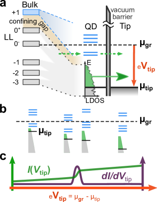
To understand the origin of the charging peaks, we provide a detailed microscopic picture of the tip-induced gating of localized states. We will only discuss the case of positive , that is, electron confinement, since the arguments for negative are analogous. Increasing (orange arrow in Fig. 3) shifts the states underneath the tip energetically down. States originating from LLs with positive index are embedded in the LL0-LL+1 gap which provides electrostatic confinement (Fig. 3a, see also Fig. 1b). Within the bias window , electrons tunnel from the sample into unoccupied states of the tip. One current path (dashed green arrow Fig. 3a) passes through states of the QD (blue lines). The other stronger current path (solid green arrow Fig. 3a) originates from the quasi-continuous LDOS at lower energies where energetically overlapping LL states strongly couple to the graphene bulk. Though increasing gates QD states down (Fig. 3b), the Coulomb gap around always separates the highest occupied from the lowest unoccupied state, prohibiting continuous charging of confined states. It is only when the next unoccupied level crosses that the QD is charged by an additional electron. The electrostatic repulsion due to its charge abruptly increases the Hartree energy of all states, thereby shifting additional graphene states from below into the bias window (Fig. 3b, central transition). Consequently, the tunneling current increases which translates to a charging peak in (Fig. 3c). This mechanism is called Coulomb staircase 40 and has been observed previously, for instance, for charging of clusters within an STM experiment 51. In essence, charging peaks in signal the coincidence of a charge level of the QD with 52 and thus provide a clear signature of the addition energy spectrum of the QD.
Since the measurement captures the QD level spacings as charging peak distances , they need to be converted to via the tip lever arm . The latter relates a change of to its induced shift of the QD state energies. The lever arm is determined by the ratio of the capacitance between tip and dot , and the total capacitance of the dot , thus . includes , the capacitance between dot and back-gate, and dot and surrounding graphene. We use a Poisson solver to estimate and for our QD (Supplement). Hence, we find and (close to values reported for a similar system by Jung et al. 33). Consequently charging peaks dominantly separated by , that is, because , should exhibit , in close agreement with the values found within quadruplets at higher occupation numbers (Fig. 2b,c). As expected, we also find significantly larger for every fourth charging peak. In case of clear quadruplet ordering, the orbital splittings for our QD are deduced from and we find typical values of for the first few orbitals (, Fig. 2b,c). For this estimate we neglect the additional Zeeman splitting or an even smaller valley splitting.
We next provide a theoretical framework to elucidate the details of the QD level spectrum. The eigenstates of bulk graphene LLs (eq 1) feature different wave function amplitudes on sublattices1 A and B,
| (2) |
where K and K’ denote the two inequivalent K-points of the Brillouin zone associated with the two valleys. For the LL index differs by one for the two sublattices, while for the part of the wave function with subscript vanishes, resulting in polarized sublattices for each valley. The wave functions of bulk graphene (eq 2) are modified by the tip-induced potential. Assuming a radially symmetric confinement potential, the eigenstates are described by radial and angular momentum quantum numbers , with and . Adiabatically mapping a given LL with index on to possible combinations of and yields 53, 54
| (3) |
with and .
We calculate eigenstates of a commensurate graphene flake on BN using third-nearest neighbor TB 38, where the substrate interaction enters via a periodic superstructure potential and local strain effects 39, parametrized from DFT calculations 55, 56. We approximate the amplitude and shape of by a classic electrostatic solution of Poisson’s equation (Fig. 1a, Supplement) with the tip radius as fit parameter. Comparing calculated charging energies to experiment yields a plausible value of implying a FWHM of the QD confinement potential of at . We independently determine the initially free parameter from the position of LL0 in STS as (Supplement). Accordingly, the graphene is p-doped. We note that varying within the stated uncertainty range (see blue horizontal bar in Figure 4a) leads to no qualitative changes in the predictions of our model. We use open boundary conditions to simulate the coupling of the flake to the surrounding graphene. Consequently, eigenstates will feature complex eigenvalues , where the real part represents the resonant energies and the imaginary part the coupling to the delocalized bulk states 57. Thus we can readily distinguish states that are spread out over the flake (large ) from those localized near the tip (small ). We color code in Figure 4a for a calculation with the tip-induced potential centered on an AB stacked area.
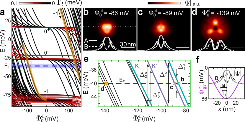
At and vanishing band bending (), we find only delocalized states whose eigenenergies cluster around the bulk LL energies (eq 1, Fig. 4a). As we increase , states begin to localize at the tip and shift in energy, with smaller (darker curves) pointing to stronger localization (see Fig. 4a). Comparing hole states originating from LL-1 for negative and positive , we find, as expected, stronger localization in case of negative . The potential is always attractive to one kind of charge carriers which will localize underneath the tip. The other kind is repelled by the induced potential (see also Ref. 31) which results in stronger coupling to the bulk. In order to classify our TB wave functions in terms of the quantum numbers , and , we consider sublattice A and B separately. Tracing the states back to their LL of origin reveals , constraining possible . The value of is then determined by counting radial minima in the line cuts of the wave function amplitude for each sublattice (Fig. 4b-d). The distance of the first radial maximum from the center of the wave function is finally sufficient to assign the possible quantum numbers of the LL (eq 3). Additionally, the () combinations need to be consistent with differing by one on the two sublattices (eq 2). For instance, the line cuts in Figure 4b portray and on sublattice A and B, respectively. As expected, small angular momentum states are the first ones to localize with increasing , in line with calculations by Giavaras et al. 30. Notice that the applied naturally lifts the orbital degeneracy in QDs 58. Delocalized states remain at bulk LL energies (red horizontal lines in Fig. 4a).
We distinguish two regimes in the sequence of spin degenerate states crossing for negative . The first regime (Fig. 4e) exhibits , while the second at higher is characterized by densely spaced states, thus . The sequence within the first regime corresponds to about five orbital pairs from valley K and K’, in line with about five quadruplets in our experimental spectra (see labels “4” in Fig. 2a and sequences in Fig. 2b,c). The quite uniform spacing of peaks for larger (Fig. 2a) agrees with the second regime. In order to extract and within the first regime, we carefully assign the valley index to the states. Using the previously determined and in eq 3, the first state crossing (Fig. 4b) features LL index on sublattice A and on sublattice B, as predicted by eq 2 for a LL|1| state in valley K. The role of the sublattices interchanges for the second state crossing (Fig. 4c), placing it in valley K’. Consequently, states with and are assigned to valleys K and K’, respectively. The calculation therefore predicts a valley splitting of about on the AB and BA areas (see Fig. 4b,c,e). is comparatively large (about ) and the respective orbital splitting is only larger by (see Fig. 4e). Consequently additional electrons may occupy the next orbital state of one valley prior to the same orbital state of the other valley at higher occupation numbers. Hence we limit further comparison to experiment to . In our TB model, the strength of the valley splitting is dominated by the sublattice symmetry breaking term due to the BN substrate 39. The calculations also show that the radial extent of the wave functions grows for the first couple of states crossing , as expected for increasing (compare Fig. 4b,c to Fig. 4d), explaining the decrease of towards higher peak indices at fixed (see Fig. 2b,c).
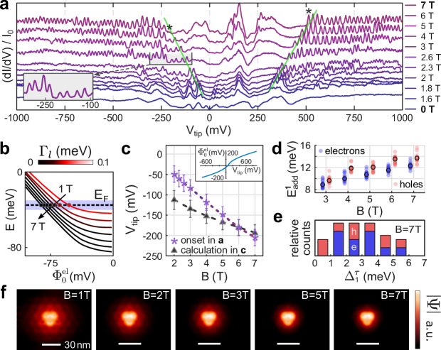
Theory and experiment can be directly compared for the dependence of the onset voltage of charging peaks . Experimentally, shifts towards higher for increasing (Fig. 5a), thus gating the first state to requires stronger band bending for higher . Since the curves for are offset proportional to , the straight line connecting the first charging peaks reveals that the energy distance of the first state to scales with . This corresponds to the increase in bulk LL energies for (eq 1), strongly suggesting those LLs as source of the confined states. This analysis is confirmed by our TB calculations, as the first crossing points of LL±1 states with the Fermi level also shift towards higher with increasing B (Fig. 5b). While the evolution of states with in Figure 4a is (approximately) symmetric with respect to , the previously discussed p-doping induces an asymmetry in for electrons and holes (see the lines highlighted in orange in Fig. 4a) and thus accounts for the observed asymmetry in . In Figure 5c we compare and by using the dependence from the Poisson solver (see inset Fig. 5c, Supplement). Care must be taken to correctly account for the work function difference between the tip and the sample: the tip’s work function ( 36, 59) exceeds that of graphene (), placing electric field neutrality in the positive sector. Moreover, it definitely has to lie in between the two charging peak regimes because the QD vanishes without band bending. Using a plausible work function difference of in Figure 5c leads to satisfactory agreement between the theoretical predictions for the first state crossings and the experimental .
Our TB simulations predict a strong reduction of with increasing magnetic field, corresponding to the suppression of the radial tail of the wave function in Figure 5f and indicating the onset of localization between 1 and (Fig. 5b). The first appearance of charging peaks in the experiment at around (Fig. 5a) fits nicely. This finding is further corroborated by comparing the diameter of the LL state , being for LL1 at , with the FWHM of the band bending region of , providing an independent confirmation of the estimated . At higher , the diameter of the first QD state wave function is dominated by rather than by the width of (Fig. 4f). The compression of the wave function for increasing (Fig. 5f) also manifests itself as increase in addition energy, for instance, for in Figure 5d, where the increase in with by about cannot be explained by that of , being between 3 and . Consequently, increased Coulomb repulsion between electrons due to stronger compression and thus larger dominates . We observe a similar monotonic increase for the other with odd index , independent of the position of the QD.
Experiment and theory also provide detailed insight into the valley splitting of the first confined states. The peaks of the first quadruplets in Figure 2a and Figure 5a (see, e.g., inset) often group in doublets, suggesting sizable values of either or (Fig. 1e,f). While is expected to be spatially homogeneous and only weakly varying between different quadruplets, the TB calculations predict strongly varying for different quadruplets (Fig. 4e), in accordance with our observations in the experimental spectra. For a quantitative comparison we focus on , which separates the two doublets within the first quadruplet. In view of the small value of the Zeeman splitting ( at ), we approximate by to extract the valley splitting . We record 20 spectra in the vicinity of an AA stacked area at to obtain a histogram of for electrons and holes (Fig. 5e), where could be determined with an experimental error smaller than . The values strikingly group around the predicted found in the TB calculations (Fig. 4e), with a probable offset in the QD position relative to the tunneling tip (Supplement, Sec. 5) explaining the QD probing an area adjacent to the tunneling tip. We conclude that sizable separate quadruplets into doublets, while the smaller contributes to the odd addition energies within the doublets. Realizing such a controlled lifting of one of the two degeneracies in graphene QDs is a key requirement for 2-qubit gate operation 2. It enables Pauli blockade in exchange driven qubits as required for scalable quantum computation approaches using graphene 2. Our observation of valley splittings, so far elusive, provides a stepping stone towards the exploitation of the presumably large coherence time of electron spins in graphene QDs 2, 3, 4, 5.
In summary, we have realized graphene quantum dots without physical edges via electrostatic confinement in magnetic field using low disorder graphene crystallographically aligned to a hexagonal boron nitride substrate. We observe more than 40 charging peaks in the hole and electron sector arranged in quadruplets due to orbital splittings. The first few peaks on the hole and electron side show an additional doublet structure traced back to lifting of the valley degeneracy. Note that such a lifting is key for the use of graphene quantum dots as spin qubits 2. Tight binding calculations quantitatively reproduce the orbital splitting energy of as well as the first orbital’s valley splitting energy of about by assuming a tip potential deduced from an electrostatic Poisson calculation. Also the onset of confinement at about is well reproduced by the calculation. Our results demonstrate a much better controlled confinement by combining magnetic and electrostatic fields than previously found in graphene. Exploiting the present approach in transport merely requires replacing the tip by a conventional electrostatic gate with a diameter of about . Moreover, the approach allows for straightforward tuning of (i) orbital splittings by changing the gate geometry and thus the confinement potential, (ii) valley splittings based on substrate interaction, (iii) the Zeeman splitting by altering the magnetic field, and (iv) the coupling of dot states to leads or to other quantum dots by changing the magnetic field or selecting a different quantum dot state. Finally, our novel mobile quantum dot enables a detailed investigation of structural details of graphene stacked on various substrates, by spatially mapping the quantum dot energies.
The authors thank C. Stampfer, R. Bindel, M. Liebmann and K. Flöhr for prolific discussions, as well as C. Holl for contributions to the Poisson calculations and A. Georgi for assisting the measurements. NMF, PN and MM gratefully acknowledge support from the Graphene Flagship (Contract No. NECTICT-604391) and the German Science foundation (Li 1050-2/2 through SPP-1459). LAC, JB and FL from the Austrian Fonds zur Förderung der wissenschaftlichen Forschung (FWF) through the SFB 041-ViCom and doctoral college Solids4Fun (W1243). Calculations were performed on the Vienna Scientific Cluster. RVG, AKG and KSN also acknowledge support from EPSRC (Towards Engineering Grand Challenges and Fellowship programs), the Royal Society, US Army Research Office, US Navy Research Office, US Airforce Research Office. KSN is also grateful to ERC for support via Synergy grant Hetero2D. AKG was supported by Lloyd’s Register Foundation.
References
- Castro Neto et al. 2009 Castro Neto, A. H.; Guinea, F.; Peres, N. M. R.; Novoselov, K. S.; Geim, A. K. Rev. Mod. Phys. 2009, 81, 109–162.
- Trauzettel et al. 2007 Trauzettel, B.; Bulaev, D. V.; Loss, D.; Burkard, G. Nat. Phys. 2007, 3, 192–196.
- Fuchs et al. 2012 Fuchs, M.; Rychkov, V.; Trauzettel, B. Phys. Rev. B 2012, 86, 085301.
- Droth and Burkard 2013 Droth, M.; Burkard, G. Phys. Rev. B 2013, 87, 205432.
- Fuchs et al. 2013 Fuchs, M.; Schliemann, J.; Trauzettel, B. Phys. Rev. B 2013, 88, 245441.
- Bischoff et al. 2015 Bischoff, D.; Varlet, A.; Simonet, P.; Eich, M.; Overweg, H. C.; Ihn, T.; Ensslin, K. Appl. Phys. Rev. 2015, 2, 031301.
- Giesbers et al. 2008 Giesbers, A. J. M.; Zeitler, U.; Neubeck, S.; Freitag, F.; Novoselov, K. S.; Maan, J. C. Solid State Commun. 2008, 147, 366–369.
- Morgenstern et al. 2016 Morgenstern, M.; Freitag, N.; Vaid, A.; Pratzer, M.; Liebmann, M. Phys. Status Solidi RRL 2016, 10, 24–38.
- Magda et al. 2014 Magda, G. Z.; Jin, X.; Hagymasi, I.; Vancso, P.; Osvath, Z.; Nemes-Incze, P.; Hwang, C.; Biro, L. P.; Tapaszto, L. Nature 2014, 514, 608–611.
- Liu et al. 2013 Liu, Z.; Ma, L.; Shi, G.; Zhou, W.; Gong, Y.; Lei, S.; Yang, X.; Zhang, J.; Yu, J.; Hackenberg, K. P.; Babakhani, A.; Idrobo, J. C.; Vajtai, R.; Lou, J.; Ajayan, P. M. Nat. Nanotechnol. 2013, 8, 119–124.
- Qi et al. 2015 Qi, Z. J.; Daniels, C.; Hong, S. J.; Park, Y. W.; Meunier, V.; Drndic, M.; Johnson, A. T. ACS Nano 2015, 9, 3510–3520.
- Vicarelli et al. 2015 Vicarelli, L.; Heerema, S. J.; Dekker, C.; Zandbergen, H. W. ACS Nano 2015, 9, 3428–3435.
- Tarucha et al. 1996 Tarucha, S.; Austing, D. G.; Honda, T.; van der Hage, R. J.; Kouwenhoven, L. P. Phys. Rev. Lett. 1996, 77, 3613–3616.
- Kouwenhoven et al. 2001 Kouwenhoven, L. P.; Austing, D. G.; Tarucha, S. Rep. Prog. Phys. 2001, 64, 701–736.
- Libisch et al. 2012 Libisch, F.; Rotter, S.; Burgdörfer, J. New J. Phys. 2012, 14, 123006.
- Bischoff et al. 2016 Bischoff, D.; Simonet, P.; Varlet, A.; Overweg, H. C.; Eich, M.; Ihn, T.; Ensslin, K. Phys. Status Solidi RRL 2016, 10, 68–74.
- Terres et al. 2016 Terres, B.; Chizhova, L. A.; Libisch, F.; Peiro, J.; Jörger, D.; Engels, S.; Girschik, A.; Watanabe, K.; Taniguchi, T.; Rotkin, S. V.; Burgdörfer, J.; Stampfer, C. Nat. Commun. 2016, 7, 11528.
- Rycerz et al. 2007 Rycerz, A.; Tworzydlo, J.; Beenakker, C. W. J. Nat. Phys. 2007, 3, 172–175.
- Recher et al. 2009 Recher, P.; Nilsson, J.; Burkard, G.; Trauzettel, B. Phys. Rev. B 2009, 79, 085407.
- Zhang et al. 2009 Zhang, Y. B.; Tang, T. T.; Girit, C.; Hao, Z.; Martin, M. C.; Zettl, A.; Crommie, M. F.; Shen, Y. R.; Wang, F. Nature 2009, 459, 820–823.
- Allen et al. 2012 Allen, M. T.; Martin, J.; Yacoby, A. Nat. Commun. 2012, 3, 934.
- Goossens et al. 2012 Goossens, A. M.; Driessen, S. C. M.; Baart, T. A.; Watanabe, K.; Taniguchi, T.; Vandersypen, L. M. K. Nano Lett. 2012, 12, 4656–4660.
- Müller et al. 2014 Müller, A.; Kaestner, B.; Hohls, F.; Weimann, T.; Pierz, K.; Schumacher, H. W. J. Appl. Phys. 2014, 115, 233710.
- Ju et al. 2015 Ju, L.; Shi, Z. W.; Nair, N.; Lv, Y. C.; Jin, C. H.; Velasco, J., Jr.; Ojeda-Aristizabal, C.; Bechtel, H. A.; Martin, M. C.; Zettl, A.; Analytis, J.; Wang, F. Nature 2015, 520, 650–655.
- Zhao et al. 2015 Zhao, Y.; Wyrick, J.; Natterer, F. D.; Rodriguez-Nieva, J. F.; Lewandowski, C.; Watanabe, K.; Taniguchi, T.; Levitov, L. S.; Zhitenev, N. B.; Stroscio, J. A. Science 2015, 348, 672–675.
- Lee et al. 2016 Lee, J.; Wong, D.; Velasco Jr, J.; Rodriguez-Nieva, J. F.; Kahn, S.; Tsai, H.-Z.; Taniguchi, T.; Watanabe, K.; Zettl, A.; Wang, F.; Levitov, L. S.; Crommie, M. F. Nat. Phys. 2016, advance online publication, DOI:10.1038/nphys3805.
- Gutierrez et al. 2016 Gutierrez, C.; Brown, L.; Kim, C.-J.; Park, J.; Pasupathy, A. N. Nat. Phys. 2016, advance online publication, DOI:10.1038/nphys3806.
- Klimov et al. 2012 Klimov, N. N.; Jung, S.; Zhu, S.; Li, T.; Wright, C. A.; Solares, S. D.; Newell, D. B.; Zhitenev, N. B.; Stroscio, J. A. Science 2012, 336, 1557–1561.
- Chen et al. 2007 Chen, H. Y.; Apalkov, V.; Chakraborty, T. Phys. Rev. Lett. 2007, 98, 186803.
- Giavaras et al. 2009 Giavaras, G.; Maksym, P. A.; Roy, M. J. Phys.: Condens. Matter 2009, 21, 102201.
- Giavaras and Nori 2012 Giavaras, G.; Nori, F. Phys. Rev. B 2012, 85, 165446.
- Moriyama et al. 2014 Moriyama, S.; Morita, Y.; Watanabe, E.; Tsuya, D. Appl. Phys. Lett. 2014, 104, 053108.
- Jung et al. 2011 Jung, S. Y.; Rutter, G. M.; Klimov, N. N.; Newell, D. B.; Calizo, I.; Walker, A. R. H.; Zhitenev, N. B.; Stroscio, J. A. Nat. Phys. 2011, 7, 245–251.
- Luican-Mayer et al. 2014 Luican-Mayer, A.; Kharitonov, M.; Li, G.; Lu, C. P.; Skachko, I.; Goncalves, A. M.; Watanabe, K.; Taniguchi, T.; Andrei, E. Y. Phys. Rev. Lett. 2014, 112, 036804.
- Tovari et al. 2016 Tovari, E.; Makk, P.; Rickhaus, P.; Schönenberger, C.; Csonka, S. Nanoscale 2016, 8, 11480–11486.
- Dombrowski et al. 1999 Dombrowski, R.; Steinebach, C.; Wittneven, C.; Morgenstern, M.; Wiesendanger, R. Phys. Rev. B 1999, 59, 8043–8048.
- Morgenstern et al. 2000 Morgenstern, M.; Haude, D.; Gudmundsson, V.; Wittneven, C.; Dombrowski, R.; Wiesendanger, R. Phys. Rev. B 2000, 62, 7257–7263.
- Libisch et al. 2010 Libisch, F.; Rotter, S.; Güttinger, J.; Stampfer, C.; Burgdörfer, J. Phys. Rev. B 2010, 81, 245411.
- Chizhova et al. 2014 Chizhova, L. A.; Libisch, F.; Burgdörfer, J. Phys. Rev. B 2014, 90, 165404.
- Averin and Likharev 1986 Averin, D. V.; Likharev, K. K. J. Low Temp. Phys. 1986, 62, 345–373.
- Mayorov et al. 2011 Mayorov, A. S.; Gorbachev, R. V.; Morozov, S. V.; Britnell, L.; Jalil, R.; Ponomarenko, L. A.; Blake, P.; Novoselov, K. S.; Watanabe, K.; Taniguchi, T.; Geim, A. K. Nano Lett. 2011, 11, 2396–2399.
- Kretinin et al. 2014 Kretinin, A. V. et al. Nano Lett. 2014, 14, 3270–3276.
- Gorbachev et al. 2014 Gorbachev, R. V.; Song, J. C.; Yu, G. L.; Kretinin, A. V.; Withers, F.; Cao, Y.; Mishchenko, A.; Grigorieva, I. V.; Novoselov, K. S.; Levitov, L. S.; Geim, A. K. Science 2014, 346, 448–51.
- Hunt et al. 2013 Hunt, B.; Sanchez-Yamagishi, J. D.; Young, A. F.; Yankowitz, M.; LeRoy, B. J.; Watanabe, K.; Taniguchi, T.; Moon, P.; Koshino, M.; Jarillo-Herrero, P.; Ashoori, R. C. Science 2013, 340, 1427–1430.
- Woods et al. 2014 Woods, C. R. et al. Nat. Phys. 2014, 10, 451–456.
- Decker et al. 2011 Decker, R.; Wang, Y.; Brar, V. W.; Regan, W.; Tsai, H. Z.; Wu, Q.; Gannett, W.; Zettl, A.; Crommie, M. F. Nano Lett. 2011, 11, 2291–2295.
- Xue et al. 2011 Xue, J. M.; Sanchez-Yamagishi, J.; Bulmash, D.; Jacquod, P.; Deshpande, A.; Watanabe, K.; Taniguchi, T.; Jarillo-Herrero, P.; LeRoy, B. J. Nat Mater 2011, 10, 282–285.
- Deshpande and LeRoy 2012 Deshpande, A.; LeRoy, B. J. Phys. E 2012, 44, 743–759.
- Mashoff et al. 2009 Mashoff, T.; Pratzer, M.; Morgenstern, M. Rev. Sci. Instrum. 2009, 80, 053702.
- Wong et al. 2015 Wong, D.; Velasco, J., Jr.; Ju, L.; Lee, J.; Kahn, S.; Tsai, H. Z.; Germany, C.; Taniguchi, T.; Watanabe, K.; Zettl, A.; Wang, F.; Crommie, M. F. Nat. Nanotechnol. 2015, 10, 949–953.
- Hanna and Tinkham 1991 Hanna, A. E.; Tinkham, M. Phys. Rev. B 1991, 44, 5919–5922.
- Wildöer et al. 1996 Wildöer, J. W. G.; van Roij, A. J. A.; Harmans, C. J. P. M.; van Kempen, H. Phys. Rev. B 1996, 53, 10695–10698.
- Schnez et al. 2008 Schnez, S.; Ensslin, K.; Sigrist, M.; Ihn, T. Phys. Rev. B 2008, 78, 195427.
- Yoshioka 2007 Yoshioka, D. J. Phys. Soc. Jpn. 2007, 76, 024718.
- Sachs et al. 2011 Sachs, B.; Wehling, T. O.; Katsnelson, M. I.; Lichtenstein, A. I. Phys. Rev. B 2011, 84, 195414.
- Martinez-Gordillo et al. 2014 Martinez-Gordillo, R.; Roche, S.; Ortmann, F.; Pruneda, M. Phys. Rev. B 2014, 89, 161401(R).
- Bischoff et al. 2014 Bischoff, D.; Libisch, F.; Burgdörfer, J.; Ihn, T.; Ensslin, K. Phys. Rev. B 2014, 90, 115405.
- Fock 1928 Fock, V. Z. Phys. 1928, 47, 446–448.
- Chen et al. 2016 Chen, Y. C.; Zhao, C. C.; Huang, F.; Zhan, R. Z.; Deng, S. Z.; Xu, N. S.; Chen, J. Sci. Rep. 2016, 6, 21270.