Evaluating Spintronic Devices Using The Modular Approach
Abstract
Over the past decade a large family of spintronic devices have been proposed as candidates for replacing CMOS for future digital logic circuits. Using the recently developed Modular Approach framework, we investigate and identify the physical bottlenecks and engineering challenges facing current spintronic devices. We then evaluate how systematic advancements in material properties and device design innovations impact the performance of spintronic devices, as a possible continuation of Moore’s Law, even though some of these projections are speculative and may require technological breakthroughs. Lastly, we illustrate the use of the Modular Approach as an exploratory tool for probabilistic networks, using superparamagnetic magnets as building blocks for such networks. These building blocks leverage the inherent physics of stochastic spin-torque switching and could provide ultra-compact and efficient hardware for beyond-Boolean computational paradigms.
Index Terms:
I Introduction
There has been enormous progress in the last few decades, effectively combining spintronics and magnetics into a powerful force that is shaping the field of memory devices, while new materials and phenomena continue to be discovered at an impressive rate [1, 2, 3, 4, 5, 6] providing an ever-increasing toolbox for the design of novel functional devices [7, 8, 9, 10, 11, 12, 13, 14]. It is natural to ask whether these developments can be harnessed to meet the increasing interest in finding new ways to meet the challenge of continuing the celebrated Moore’s law in the coming decades.
Broadly speaking the relevant developments in spintronic materials and phenomena belong in two categories, those that enable conversion of electrical into magnetic information (the WRITE function) and those that enable the reverse process (the READ function). READ and WRITE functions are of course central to memory devices and it has also been shown that they can be integrated into a transistor-like device, with gain and input-output isolation, that we call a “spin switch” which can be used as a building block for logic circuits [8, 15].
A natural question to ask is how such a spin switch compares with a standard switch based on CMOS (complementary metal oxide semiconductor) technology, and several authors have addressed different aspects of this question [16, 17, 18, 19]. The purpose of this paper is to establish a systematic framework for evaluating the impact of different READ and WRITE units on the key performance criteria for logic devices, namely their static power consumption, switching energy, switching delay and the energy-delay product. This framework is based on Modular Approach to Spintronics [20, 21] whereby different materials and phenomena are represented by experimentally benchmarked modules, whose input and output voltages and currents have four components, one for charge and three for spin (fig. 1a). These modules can then be combined using standard SPICE or SPICE-like platforms to evaluate circuit and system level performance.
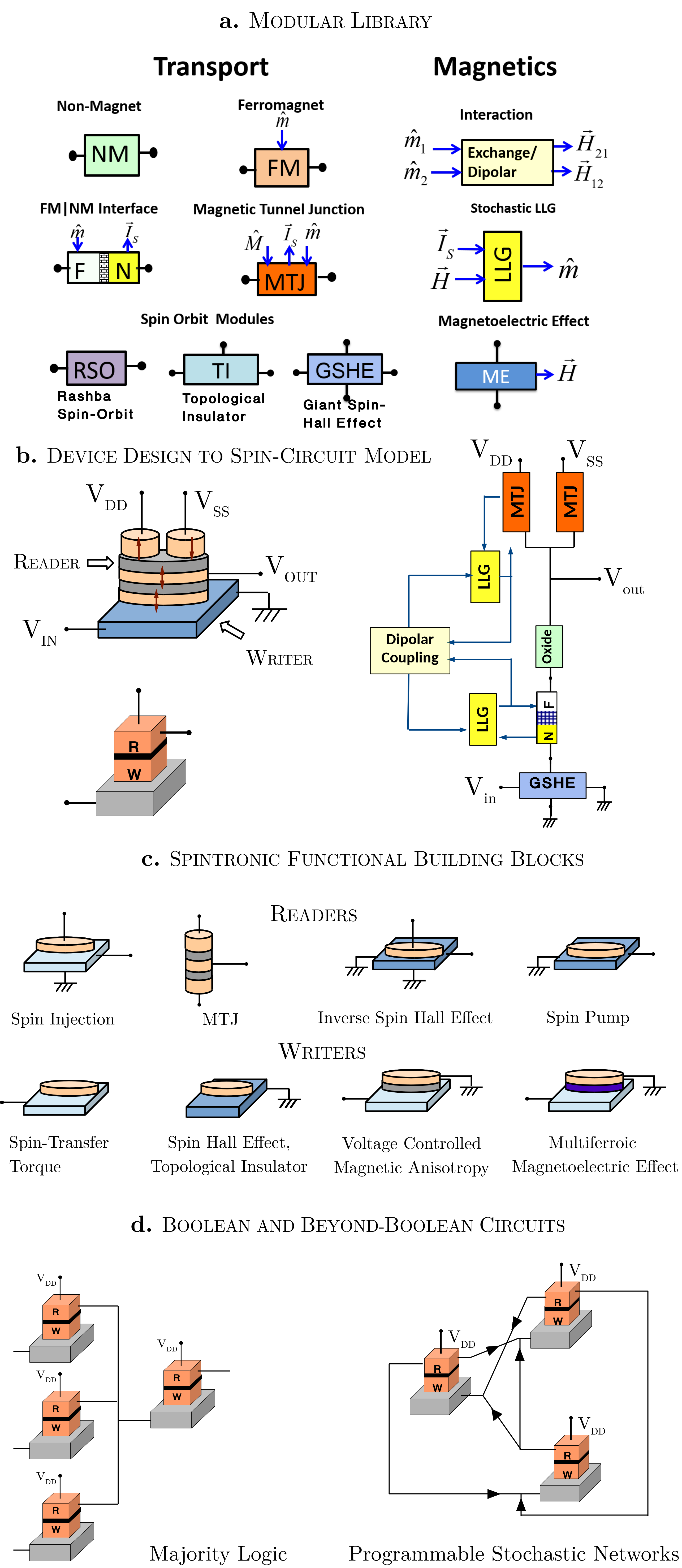
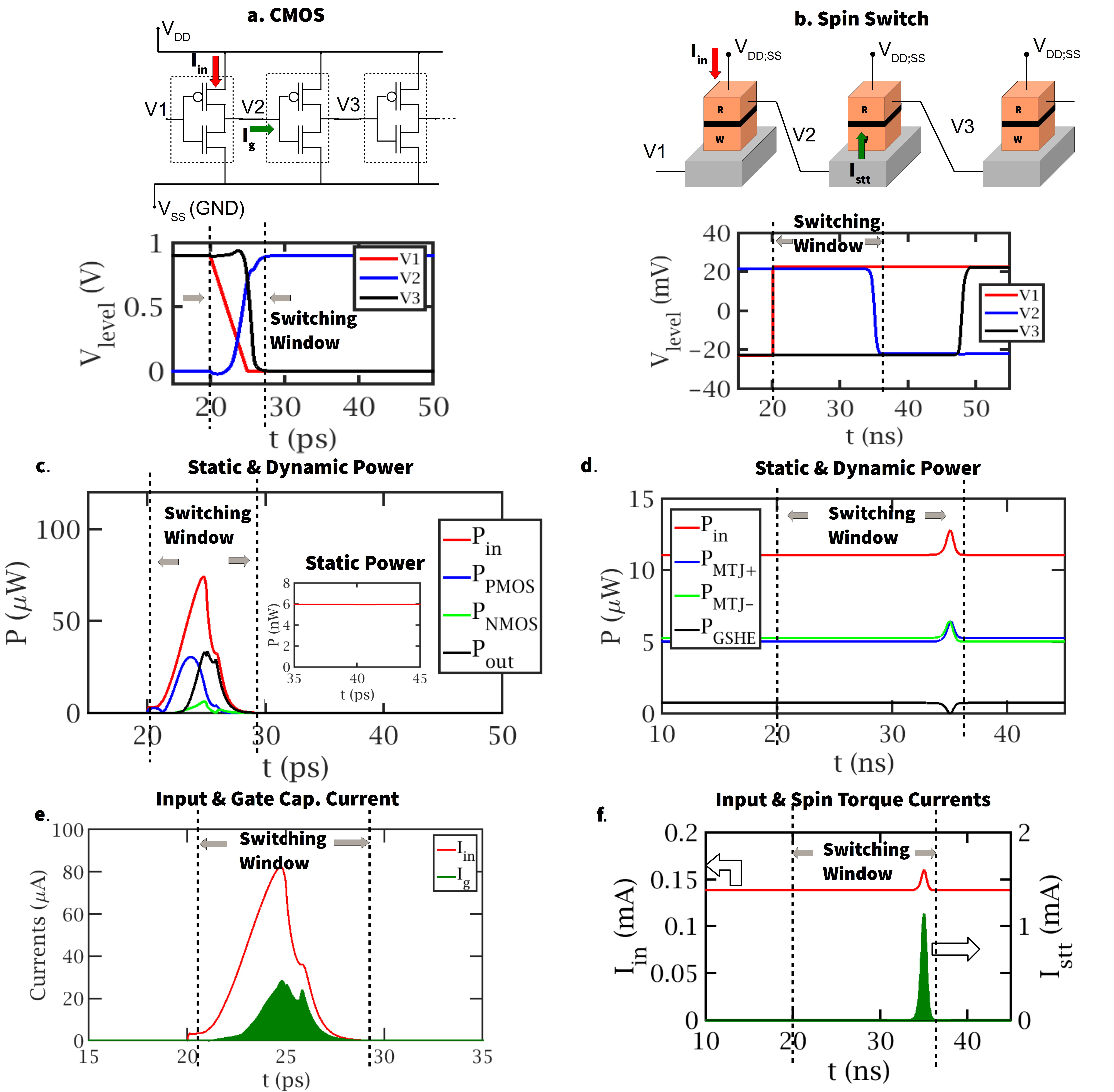
In Section II, we analyze a series of spin switches based on a magnetic tunnel junction (MTJ) for the reader and the spin Hall effect (SHE) for the writer providing a direct comparison of switching currents and power with a series of CMOS inverters (fig. 1b). The purpose is to pinpoint the factors underlying the inferior static power and energy-delay product of spin switches relative to a CMOS switch. In Section III using modular approach we evaluate spin switches utilizing several alternative readers and writers (fig. 1c) which show a potential improvement in performance that could be comparable CMOS if optimistic material performance and integration parameters are realized in the future.
Since Moore’s law has been made possible by a doubling of the number of switches in a given area every two years, this cannot continue without a significant reduction in the energy-delay product relative to CMOS which seems difficult based on present state-of-the-art in spintronics. However, it has been noted that from a consumer perspective, Moore’s law represents a doubling of “user value” every two years and this could be enabled through enhanced functionality [22]. It has been recognized that nanomagnets could provide enhanced functionality over CMOS through their unique physics that provides a natural bistability, threshold response and stochastic operation.
We end in Section IV with an evaluation of a simple version of a restricted Boltzmann machine featuring stochastic spin switches (fig. 1d) and is similar to other examples of usage of stochasticity of magnets for computing [23, 24, 25, 26]. Such “stochastic computers” are commonly implemented virtually using software algorithms on a deterministic hardware platform, but nanomagnets could provide a natural physical hardware for their efficient implementation [27, 28, 29]. A detailed evaluation of different options and possibilities is beyond the scope of this paper. Our purpose here is simply to use the Modular Approach to establish a common framework for connecting from basic materials and phenomena all the way to circuits and systems, both deterministic and stochastic.
II Spin-Switches vs. CMOS
In this section we use the original proposal of the spin switch [8] as an example to examine the physics of power dissipation in spintronic devices. The spin switch uses an MTJ stack for READ, while WRITE is through a GSHE layer driving a ferromagnet (FM) coupled magnetically to the MTJ, providing electrical isolation and coupling, while the GSHE-based writing provides gain. In section III, we systematically go through other variations and possibilities of READ/WRITE units that can be used to build a family of spin switches.
As a reference point, we have used a CMOS inverter built from ASU-PTM models for 14nm HP-FinFETs [30, 31] to highlight the differences and similarities between physics of switching and power dissipation in both charge based and spin based devices. Fig. 2a,b shows a FO-1 inverter chain built using CMOS and the spin-switch respectively. Details on simulation parameters are shown in the supplementary. For details on spin-circuit modeling and to obtain open-source circuit models of the devices used in this work, please see [21].
II-A Static Dissipation
Static power dissipation is the Joule heating () losses at steady state, i.e. when the device is not switching. It is a critical measure of device performance, since this contributes to the thermal budget of any circuit built using the device.
Insets in fig. 2c,d show a typical switching transient and toggling of the voltages causally () in the logic pipeline. The supply voltage levels used in HP-CMOS are typically , whereas in spin-switch at minimal overdrive, it can range from and is sufficient to generate the threshold spin current necessary () to switch a typical nanomagnet with a 40 stability, given the characteristic resistances of all the components (GSHE, MTJ) are around (A complete list of parameters are shown in the supplementary).
The static power levels in HP-CMOS are of the order of (fig. 2c) as expected from the leakage current levels [32], which is much lower compared to dynamic power levels. However, the static power dissipation in spin-switch is nearly the same as the dynamic power dissipation because the spin-switch does not turn off at steady state (fig.2d). There is a constant current flow through the MTJs, since the resistance ratio of the MTJ pair is , compared to CMOS where of the PMOSNMOS pair is .
Additionally, the input side of the spin-switch (GSHE) is a low impedance component, unlike the CMOS where the MOSFET gate terminals are high impedance components that become open circuit at steady state. As a result of these two static current flows, the static power dissipation remains near levels for the spin-switch.
II-B Dynamic Dissipation: Energy Delay
Any alternative to CMOS needs to be competitive in terms of both the switching delay and switching energy. A useful measure of dynamic dissipation is the product of the switching energy switching delay ( product) per switching event, because a switch can be overdriven for lower switching delay, resulting in higher switching energy or vice versa. It has been shown [33] that the product can be related to the charge consumed during the switching process, i.e. , where is the charge drawn over the effective resistance to switch the device. The metric recast as provides a powerful approach to understanding the fundamental limits of dynamic dissipation in a device by quantitatively relating it to its physical properties and opens a pathway to better component design for higher performance.
II-B1 Switching Delay
The timescale of switching in a scaled CMOS inverter, a 14 nm FinFET in this case, is of the order of (fig. 2a). The switching delay for magnets is dependent on the current overdrive: At large overdrives the delay can be determined by angular momentum considerations, where a total amount of charge that is twice the number of spins () needs to be deposited for a complete reversal of magnetization. This means that the switching delay inversely scales with the driving current, i.e. . The exact switching delay is a strong function of the initial angle of the magnetization [34]. In our simulations, the initial angle is chosen to be the rms of the equilibrium deviation from the easy axis [7].
II-B2 Switching Energy and Switching Charge
Switching energy in itself can be calculated by simply integrating the power between the switching window. While this approach does work numerically, to gain better physical understanding of dynamic dissipation, we look at the switching charge, as discussed at the beginning of the section. To do so from our circuit testbench, we first integrate the input current (red arrows indicated in fig. 2a,b) supplied from the sources within the switching window, whose starting point is the the time-point at which the input signal signal starts changing and the ending point is the time-point at which the output signal is within of its final value. This provides the total charge per switching event. Additionally, we integrate the total current deposited to the CMOS input terminals (gates) and we do the same for the analogous quantity for magnets, the z-component of the spin-torque current () which are indicated by the green arrows in fig.2b.
We find that the area under the green curve for the CMOS (fig. 2e) is about , equivalent to the charge deposited to the CMOS gates , whereas the green area for the spin-switch (fig. 2f) is about where is the total number of spins (. Therefore, reducing the dynamic dissipation for any logic device involves scaling the through better component design[35, 36].
It should be noted that the in our discussion this far is only an approximate measure of since it does not incorporate the steady state currents discussed in static dissipation section, as well as any load driven by the device at the fanout. Using our methodology, we can relate the to the total charge provided by the supply. As an example in fig. 2f, the area under the red curve integrated in the switching window, gives the total charge pumped in by both the supplies () during one switching event. This area is about 10 times the green area which gives the , in the case of spin-switch. For the CMOS inverter (fig. 2e), the total charge pumped is about 6 times the . Any improvement in scaling down the dynamic dissipation will then involve reducing the as well the during switching.
| Metric | HP-CMOS | Spin-Switch |
|---|---|---|
| Voltage Level | ||
| Static Power | ||
| Dynamic Power | ||
| Switching Delay | ||
| Switching Charge, | ||
| / |
We summarize the metrics discussed in this section in Table. I. While the details of the physics in these examples depend on the specifics of circuit design, material parameters and overdrive conditions, we believe that the measure of static power in terms of (READ) and dynamic power in terms of (WRITE) are general notions that should be applicable to any logic device.
III Alternative Designs for Spin-Switch
In this section, we show how the spin-switch device can be made competitive with CMOS inverter through improvements in device materials, magnetic stack designs, and use of different components based on new phenomena. This allows us to project performance enhancements quantitatively and build possible roadmaps for optimized spin-switch devices. We have covered only a small sampling of possible optimization and design space for spintronic devices. Our main purpose is to demonstrate the power of Modular Approach in building and evaluating alternative designs.
III-A Alternative Design Trajectories
We show 3 example trajectories of how the spin-switch can be optimized by stacking one change on top of the other and observe its effect in reducing the static and the dynamic dissipation. The next few headings describe the changes we introduce to the spin switch design sequentially. While each of these improvements can be applied independent of each other, the presented information shows how the performance of the spin-switch can improve dramatically when these optimizations are applied in succession.
The numbers reported in this section are from the measurements of static power, switching energy and switching delay performed for an FO-1 circuit testbench, as described in the supplementary. These numbers would vary if a different testbench, such as FO-4 or 32-bit adder, is chosen, since it will change the loading conditions. While some of the low spin-switch designs could work with ultra low voltages (), a conventional circuit may not be able to provide due to the inability to deliver sufficient power at such low voltages [37]. Additional transistors could be used in conjunction with each spin-switch to obtain lower voltages and such transistors will have their own dissipation. We have used a minimum supply voltage level of in some of the alternative designs but do not include dissipation numbers of transistors in such cases. Furthermore, in this work our analyses are limited to the devices themselves and we do not measure dissipation in interconnect and supply rails as well as the driver circuitry consisting of CMOS devices. All the material parameters used in these simulations are listed in the supplementary and are optimistic projections which may not have been demonstrated at present. We also list theoretical minimum operating points for the spin switch designs discussed in this section based on analytical model for these devices and the material parameters.
III-A1 Magnet DesignIMA to PMA
The first improvement we make to the device design is the replacement of magnets with in-plane magnetic anisotropy (IMA) with perpendicular magnetic anisotropy (PMA). This reduces the minimum switching current required by getting rid of the large demagnetizing field () while maintaining the barrier height , since in the monodomain approximation, the in-plane minimum switching current is given by [34]:
| (1) |
However, in the case of GSHE-based switching employing PMA magnets introduces the well-known problem of indeterministic switching, since the polarization of the injected spin-current from the GSHE is in the in-plane direction, thereby bringing the magnetization of the free layer to the in-plane hard axis, an unstable equilibrium position. A small magnetic field () in the direction of the charge current helps break the symmetry of this equilibrium position and push the magnetization towards an easy axis. This field may be provided either locally [38] or as a small exchange-bias field built within the structure of the magnetic stack [39]. We incorporate this field in our model simply as an additional external field provided to the LLG modules in the spin-circuit model.
In this case, the minimum spin-current necessary to switch the magnet is approximately given by [40]:
| (2) |
It is interesting to note that the threshold current for “hard-axis” switching does not benefit from a one to two orders of magnitude reduction due to the absence of the damping factor that is present in eq. 1.
III-A2 Magnet DesignHigh Anisotropy Scaled PMA
Using PMA magnets in spin-switch opens up the possibility of using high anisotropy magnets commonly used in the magnetic recording industry. This is achieved by scaling down the grain volume () and saturation magnetization () while increasing the effective anisotropy () to maintain a given thermal stability since the barrier height is given by . While the minimum spin-current necessary to switch remains the same (eq. 2), the supply voltage levels to produce the minimum switching current increase as compared to unscaled PMA magnets due to two reasons: (a) increase in the resistance of the GSHE writer and (b) reduction of the geometrical gain due to a decrease in the length of the GSHE metal.
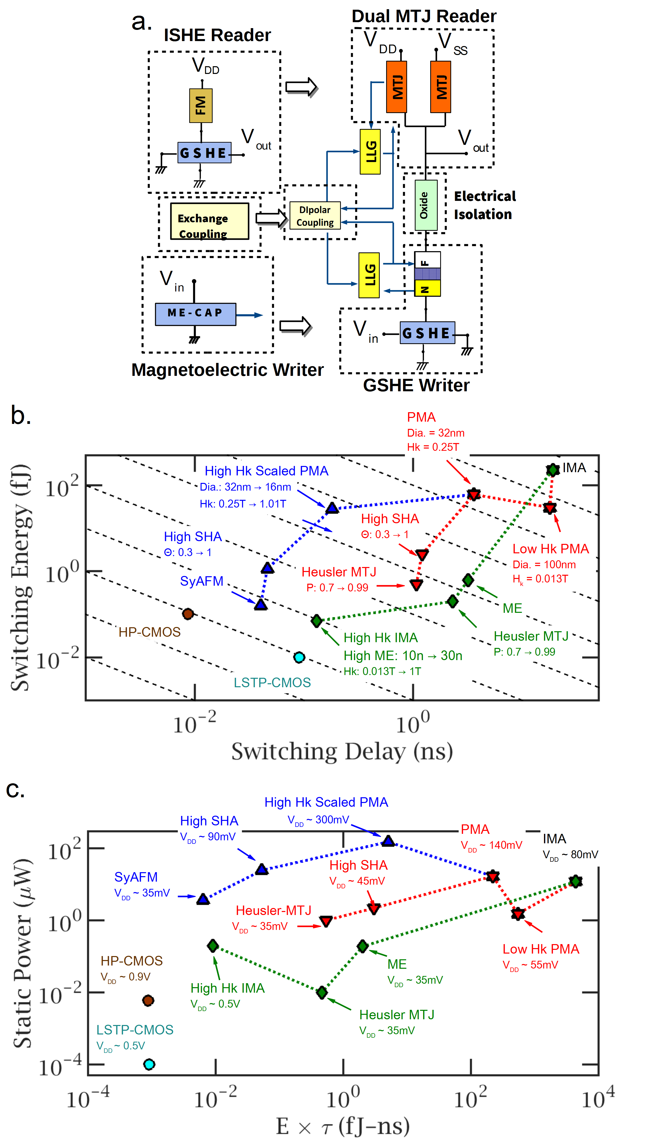
However, using high and low reduce switching charge () in the magnet, significantly improving the energy-delay as shown in fig. 3b, since . On the other hand, the reduction in comes at a cost of increase in the static power (fig. 3c) due to increased supply voltages, as shown in both red (medium scaled PMA) and blue (high scaled PMA) trajectories.
Increasing the of the magnets could necessitate changing the coupling mechanism between the WRITE and the READ units, since dipolar coupling may not provide strong enough interaction necessary for successful device operation. Advancements in magnetic oxides may open a pathway for stronger exchange-interaction based coupling of high magnets through either indirect exchange coupling mediated through the magnetic oxide [41] or by replacing the metallic FM with an insulating FM [42]. However, the thickness of the oxide layer necessary to provide exchange coupling is a critical issues that may interfere with the electrical isolation of the WRITE and the READ units through leakage currents due to tunneling effect, forming a parasitic MTJ between them. Our analysis presented here did not account for this leakage current in the coupling layer. Additionally, fabricating and creating contacts on highly scaled device could have lithographic challenges that may require change in the device design of the spin switch and is out of scope for our present study. Our focus here is to show how Modular Approach can be used to project performance enhancement assuming such challenges could be met.
III-A3 Reader Design Heusler Alloys
A major improvement that can be incorporated in the spin-switch designs is the use of high polarization magnets (such as Heusler alloys) to fabricate MTJ or Spin-Valve based readers through an increase of . It can be shown from TMR formula () that to achieve the same ratio as a well designed CMOS inverter (), the interface polarization that would be required is . For the sake of performance projection we choose an optimistic value of (close to an experimentally reported value of at low temperatures [6]) which gives .
Use of Heusler alloys helps in reducing the static power loss in the reader by reducing the supply voltages and bringing closer to the supply voltages (fig. 3a). However, the high of the MTJ reader imposes a limit on the overdrive that can be applied to the spin-switch, because the spin-current generated in the MTJ may start switching the device in competition with the GSHE writer, especially in scaled spin-switches where the geometrical gain in GSHE given by is limited by scalability of GSHE thickness and spin-flip length compared to length [43].
III-A4 Writer DesignHigh Spin Hall Angle
Using materials with large spin Hall angles can help in scaled spin-switches by lowering the voltage levels, since smaller charge currents can produce larger spin-current. For projection purposes, we choose a spin-Hall angle of . In both blue (high scaled PMA) and red (medium scaled PMA) trajectories in fig. 3b and fig. 3c, the is reduced by two orders of magnitude and static dissipation is reduced by one order of magnitude due to lower supply voltage levels.
We have assumed that the resistance of the GSHE material remains the same during this optimization, which is not necessarily true. In fact it has been suggested that resistance of most GSHE materials increase hand in hand with the Hall angle [43], and this may reduce the magnitude of the and static power improvements projected. However, it was recently suggested that using a composite structure consisting of a spin conduction layer between the GSHE and the magnet, it may be possible to obtain large spin-Hall angles from small spin-Hall angle materials [44]. Such innovations in device engineering could provide a way to obtain large spin-Hall angles without the large resistance penalty.
III-A5 Writer DesignSpin Torque vs. Magnetoelectrics
Instead of the spin-torque mechanism, voltage-controlled magnetoelectric (ME) phenomena based on multiferroic materials could be used for the WRITE in a spin-switch. In particular, (BFO) was recently shown to be capable of switching an IMA magnet deterministically [4] by applying a voltage controllable exchange bias field on the adjacent magnetic layer. Indeed, various device proposals have used this mechanism as part of their device designs [11, 45, 46].
The switching process using ME fundamentally requires only amount of charge, where is the capacitance of the ME material and is the applied voltage. Since the switching mechanism is not spin-torque, it can be much smaller compared to , opening a pathway for much more efficient switching. This phenomenon is also attractive because it creates a high input impedance device similar to a CMOS inverter and reduces static dissipation. Indeed, it is seen in fig. 3b and fig. 3c that the green trajectory that replacing the GSHE writer with an ME based writer reduces both and static power drastically.
The ME module used in this work does not consider the ferroelectric polarization caused by the electric field and hence is not a comprehensive model for the multiferroic material. Additionally, the dynamics of the ME based switching was deduced to be a complex 2-step process composed of two partial switchings in two different directions, ultimately causing a full reversal in the experiment [4]. Coupling the LLG with an ME module produces only a single step switching. Since the detailed physics of multiferroic switching is not fully understood at this time, these projections are subject to change as a better understanding of voltage based multiferoic switching develops.
III-A6 Magnetic Stack Design Synthetic Ferrimagnets
Usage of synthetic ferrimagnet (SyAFM) stacks instead of monolayer magnets opens up an avenue of performance improvement of the spin-switch. This is due to a reduction in the effective switching charge (), where () compared to a monodomain magnet () with the same thermal stability, for details see [36]. In the blue trajectories (high scaled PMA) of fig. 3b and fig. 3c we use an SyAFM stack where . This provides an order of magnitude improvement in alongside a reduction of voltage levels by which helps reduce the static power. Optimized designs of SyAFM stacks may yield even higher performance gains.
III-B Outlook for the Spin-Switch
Overall we find that spin-switches may approach the performance of contemporary scaled FinFET based CMOS if integration of various high performance materials along with careful device engineering and advanced lithographic and fabrication abilities can be achieved. Meanwhile, CMOS technology itself is a moving target, considering recent developments such as negative capacitance [47], therefore it will be difficult for an individual spin device to outperform the CMOS inverter in the near future.
Natural domain of spintronics may be in complex circuits where the inherent physics of a single device can map to a higher order logic function that requires many basic logic gates to implement, as argued in [48]. These devices can then be deployed as compact and efficient computational nodes in complex Boolean and Beyond-Boolean architectures. The next sections explore this possibility using simple proof of concept demonstration.
IV Beyond Boolean Circuits: Spintronic Probabilistic Networks
A big thrust of spintronic research is the use of spin devices as ultra-compact deterministic nodes of hardware neural networks [49, 50, 51] due to inherent majority logic-like behavior (detailed analysis of such a compact majority logic circuit is provided in the supplementary). In this respect, the advantage of spin-switch as nodes of neural networks primarily lie in their ability to reduce dissipation and simpler circuit design due to reduced hardware cost compared to CMOS based implementations. In this section we go beyond the applications of spin-switch as neural network nodes and look at the physics of stochasticity of superparamagnets and its applications in the emerging field of probabilistic spintronic logic [29].
IV-A Stochastic Magnet Dynamics
Our spin-switch designs discussed up to this point have used magnets with with state retention of nearly a decade. The state retention and barrier height is related by , where . Even though we have not explicitly concerned thermal noise in our analysis so far, when , there is only a minor effect on the switching dynamics due to thermal agitation, and the switching delay is largely determined by the initial angle of the magnet. We have approximately taken this initial angle variation into consideration by using mean initial angles that are in consistent with results from equilibrium statistical mechanics [52].
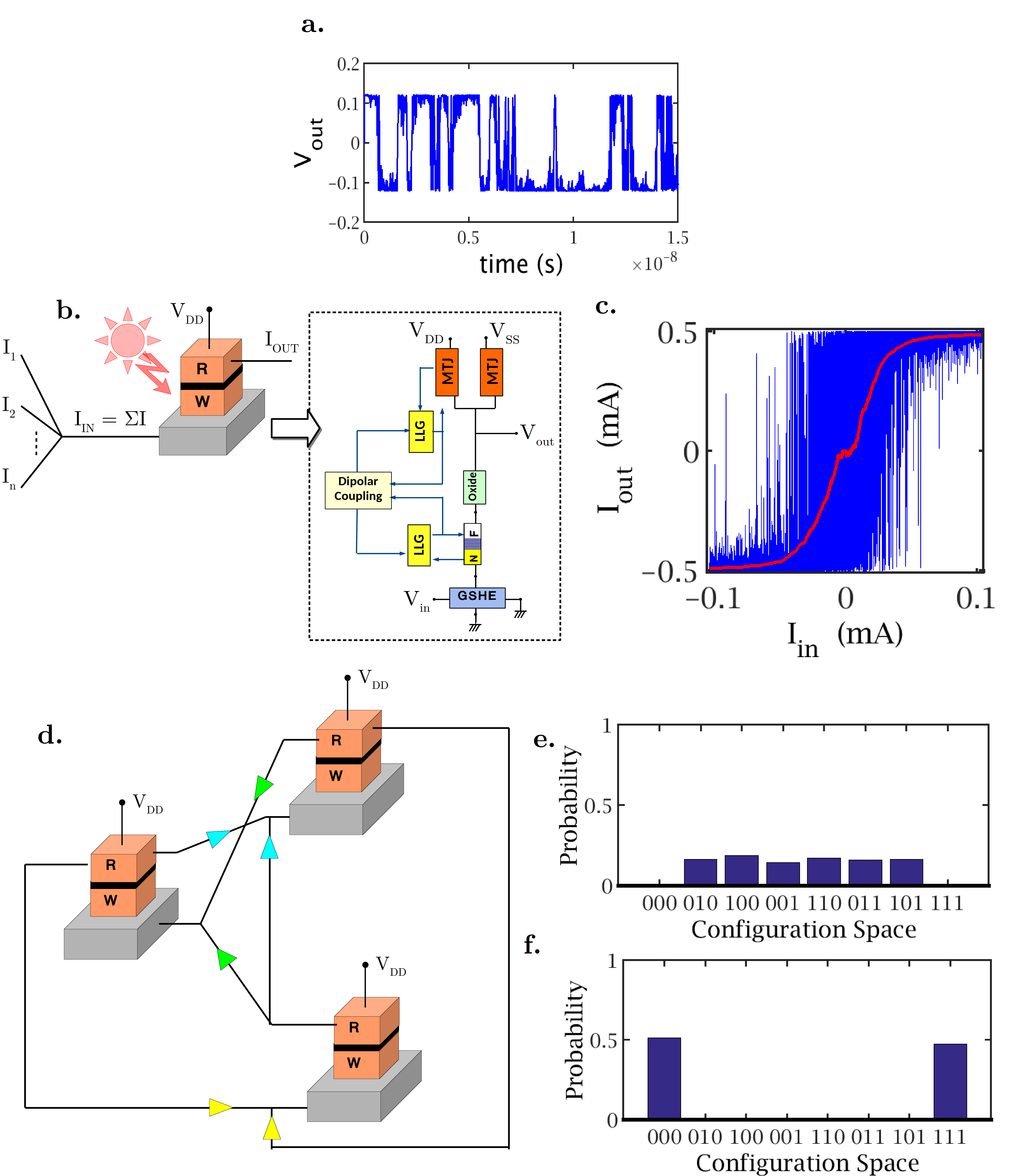
However, reducing the barrier height of these ferromagnets to superparagmagnetic values, for example , makes the magnetization stochastic and the statistical average of the magnetization lies between “up” and “down” states. As an example, fig. 4a shows a transient simulation of a magnet with only under the influence of a thermal noise field. The magnetization keeps flipping back and forth between the up and down states, since the state retention time is of the order of . This stochastic behavior along with spin-torque or magnetic field switching can yield building blocks for probabilistic computers [27, 28, 29] where probabilistic behavior comes naturally due to inherent physics of the device itself.
IV-B Stochastic Spin Switch: Building Block of Probabilistic Networks
Fig. 4b shows a stochastic spin-switch operating under room temperature conditions. As explained in the previous section, the spin-switch naturally accumulates multiple input signals at its input node (analogous to synaptic addition in a neuron) and switches. When this switching happens at a finite temperature, the output of the neuron instead of being a deterministic function whose output is “0” or “1”, instead turns into a stochastic one whose average is skewed by the input current (blue background curve in fig. 4c). This output when passed through a simple R-C low pass filter circuit ( in the simulation) that extracts the average value produces a transfer function which instead of being a sharp transition, turns into a sigmoidal function (red foreground curve in fig. 4c), useful for building probabilistic and fuzzy logic circuits.
The stochastic regime of operation of the spin-switch and its use as a building block for probablistic networks was first identified in [27], where it was called a transynapse. The major distinction between the previous work and this paper is our use of spin-switches with in-plane magnets in the superparamagnetic regime and a time-averaged measurement, rather than averaging an ensemble of thermally stable magnets undergoing hard axis switching, following [28, 53]. Since the computation with stochastic spin-switch is statistical unlike deterministic switching, a direct comparison of performance with another technology is highly implementation dependent and is not attempted here. Our main purpose is to demonstrate how the Modular Approach enables the exploration of stochastic spin-switches to build novel beyond-Boolean circuits.
IV-C Programmable Stochastic Networks
By connecting the stochastic spin switches together we can create novel beyond Boolean circuits, an example being the Ising network, a computational model that is widely used to solve complex optimization and pattern recognition problems [54]. The nodes of the network interact with each other through the charge currents in the GSHE, which can be controlled by either changing the voltage between the nodes (through sign and magnitude) or by using an external CMOS circuitry. The network can then be annealed to its ground state providing a solution of the problem. While the Ising model in itself is purely deterministic, stochasticity of the superparamagnets helps the system to traverse the configuration space of the network at the speed of the magnet retention time, which could be a few or less for superparamagnets.
As an example, fig. 4e,f shows two different solutions mapped in the steady state statistical configuration of the 3-node Ising network (fig. 4d), ferromagnetic and frustrated spin-glass. These two configurations can be obtained by tuning the interaction strength and sign between the three nodes. One way to achieve this is by an external circuitry that implements a weighing logic of the form where is the input voltage for the node, is the output of the node and is the weight logic and the elements of the Ising Hamiltonian for the given problem. In this problem and all positive creates ferromagnetic interaction, whereas all negative creates anti-ferromagnetic interaction. The magnitude of the is chosen to ensure that the average output of the nodes are in the “saturated” region of the fig. 4a. The circuit is simulated in presence of magnetic thermal noise and the temperature of the system reduced slowly to anneal the circuit to its ground state. The time duration of these simulations were chosen to be three orders of magnitude higher compared to the state retention time of the superparamagnets to obtain stable statistics. The ref. [28] explains the simulation technique in more detail.
If the interactions are tuned to make the network ferromagnetic, the configuration space obtained after a time averaged measurement is shown in fig. 4f where nodes prefer the or state, i.e. all of the nodes are in the same state. However, for antiferromagnetic interaction, the nodes take up the other 6 possible states equally distributed statistically (fig. 4f), forming a frustrated spin-glass, since the interaction strengths are equal in this simulation.
This proof of concept demonstration points towards a possibility of building larger dynamically programmable stochastic networks (as in [28, 29]) that solve algorithms of data mining, optimization, searching, and machine learning (Deep Belief Networks) which at present are commercially implemented as software solutions. These stochastic networks map complex and composite logic functions directly into the physics of the spintronics, paving the way of creating ultra-compact and efficient learning networks.
V Conclusion
In this paper, we have performed a systematic analysis of a family of spin-based logic devices using the recently developed Modular Approach framework. By making materials, device and circuit level projections, we have estimated critical circuit metrics such as dynamic (WRITE unit) and static (READ unit) power dissipation of concrete designs and compared them to existing CMOS technology. With very optimistic material and design parameters that would only be available with several technological breakthroughs in the field, such as Heusler alloys and high spin Hall angles, we find that spin-based logic devices could have energy-delay products comparable to CMOS technology. Besides there are factors such as non-volatility that are not captured by the energy-delay product.
It is important to point out however, given the enormous rate of discoveries in the field, it is very likely that the conclusions presented in this paper will quickly need to be updated, and as such, one of the key objectives of this paper was to illustrate how the Modular Approach framework can reliably integrate emerging physics into existing physics at the device and circuit level.
As an example of the versatility of the modular approach, we show that even for beyond-Boolean architectures different from what is conventionally discussed in spin-logic proposals, the same framework allows systems-level analyses, once an experimentally benchmarked module for the relevant building blocks (superparamagnets in this case) is available.
Acknowledgment
The authors would like to extend their thanks to Dr. Behtash Behin-Aein for sharing his preprint [27] and for helpful discussions on programmable stochastic networks. The authors would also like to thank Dr. Azad Naeemi for helpful discussions on engineering challenges with the spin-switch and the alternative designs. This work was supported in part by the National Science Foundation through the NCN-NEEDS program, contract 1227020-EEC and in part by C-SPIN, one of six centers of STARnet, a Semiconductor Research Corporation program, sponsored by MARCO and DARPA.
References
- [1] I. Mihai Miron, G. Gaudin, S. Auffret, B. Rodmacq, A. Schuhl, S. Pizzini, J. Vogel, and P. Gambardella, “Current-driven spin torque induced by the Rashba effect in a ferromagnetic metal layer,” Nat Mater, vol. 9, no. 3, pp. 230–234, Mar. 2010.
- [2] L. Liu, C.-F. Pai, Y. Li, H. W. Tseng, D. C. Ralph, and R. A. Buhrman, “Spin-Torque Switching with the Giant Spin Hall Effect of Tantalum,” Science, vol. 336, no. 6081, pp. 555–558, May 2012.
- [3] Y. L. Chen, J. G. Analytis, J.-H. Chu, Z. K. Liu, S.-K. Mo, X. L. Qi, H. J. Zhang, D. H. Lu, X. Dai, Z. Fang, S. C. Zhang, I. R. Fisher, Z. Hussain, and Z.-X. Shen, “Experimental Realization of a Three-Dimensional Topological Insulator, Bi2Te3,” Science, vol. 325, no. 5937, pp. 178–181, Jul. 2009.
- [4] J. T. Heron, J. L. Bosse, Q. He, Y. Gao, M. Trassin, L. Ye, J. D. Clarkson, C. Wang, J. Liu, S. Salahuddin, D. C. Ralph, D. G. Schlom, J. Íñiguez, B. D. Huey, and R. Ramesh, “Deterministic switching of ferromagnetism at room temperature using an electric field,” Nature, vol. 516, no. 7531, pp. 370–373, Dec. 2014.
- [5] W.-G. Wang, M. Li, S. Hageman, and C. L. Chien, “Electric-field-assisted switching in magnetic tunnel junctions,” Nat Mater, vol. 11, no. 1, pp. 64–68, Jan. 2012.
- [6] H.-x. Liu, Y. Honda, T. Taira, K.-i. Matsuda, M. Arita, T. Uemura, and M. Yamamoto, “Giant tunneling magnetoresistance in epitaxial Co2MnSi/MgO/Co2MnSi magnetic tunnel junctions by half-metallicity of Co2MnSi and coherent tunneling,” Applied Physics Letters, vol. 101, no. 13, p. 132418, 2012.
- [7] B. Behin-Aein, D. Datta, S. Salahuddin, and S. Datta, “Proposal for an all-spin logic device with built-in memory,” Nat Nano, vol. 5, no. 4, pp. 266–270, Apr. 2010.
- [8] S. Datta, S. Salahuddin, and B. Behin-Aein, “Non-volatile spin switch for Boolean and non-Boolean logic,” Applied Physics Letters, vol. 101, no. 25, p. 252411, Dec. 2012.
- [9] D. E. Nikonov, G. I. Bourianoff, and T. Ghani, “Proposal of a Spin Torque Majority Gate Logic,” IEEE Electron Device Letters, vol. 32, no. 8, pp. 1128–1130, Aug. 2011.
- [10] J. G. J. Zhu, D. M. Bromberg, M. Moneck, V. Sokalski, and L. Pileggi, “mLogic: All spin logic device and circuits,” in 2015 Fourth Berkeley Symposium on Energy Efficient Electronic Systems (E3S), Oct. 2015, pp. 1–2.
- [11] S. Manipatruni, D. E. Nikonov, and I. A. Young, “Spin-Orbit Logic with Magnetoelectric Nodes: A Scalable Charge Mediated Nonvolatile Spintronic Logic,” arXiv:1512.05428 [cond-mat], Dec. 2015, arXiv: 1512.05428.
- [12] M. C. Chen, Y. Kim, K. Yogendra, and K. Roy, “Domino-Style Spin #x2013;Orbit Torque-Based Spin Logic,” IEEE Magnetics Letters, vol. 6, pp. 1–4, 2015.
- [13] K. Roy, S. Bandyopadhyay, and J. Atulasimha, “Hybrid spintronics and straintronics: A magnetic technology for ultra low energy computing and signal processing,” Applied Physics Letters, vol. 99, no. 6, p. 063108, Aug. 2011.
- [14] A. Imre, G. Csaba, L. Ji, A. Orlov, G. H. Bernstein, and W. Porod, “Majority Logic Gate for Magnetic Quantum-Dot Cellular Automata,” Science, vol. 311, no. 5758, pp. 205–208, Jan. 2006.
- [15] S. Datta, V. Q. Diep, and B. Behin-Aein, “What constitutes a nanoswitch? A Perspective,” arXiv:1404.2254 [cond-mat], Apr. 2014, arXiv: 1404.2254.
- [16] D. Nikonov and I. Young, “Benchmarking of Beyond-CMOS Exploratory Devices for Logic Integrated Circuits,” IEEE Journal on Exploratory Solid-State Computational Devices and Circuits, vol. 1, pp. 3–11, Dec. 2015.
- [17] J. Kim, A. Paul, P. A. Crowell, S. J. Koester, S. S. Sapatnekar, J. P. Wang, and C. H. Kim, “Spin-Based Computing: Device Concepts, Current Status, and a Case Study on a High-Performance Microprocessor,” Proceedings of the IEEE, vol. 103, no. 1, pp. 106–130, Jan. 2015.
- [18] S. Manipatruni, D. E. Nikonov, and I. A. Young, “Material Targets for Scaling All-Spin Logic,” Phys. Rev. Applied, vol. 5, no. 1, p. 014002, Jan. 2016.
- [19] S. C. Chang, N. Kani, S. Manipatruni, D. Nikonov, I. Young, and A. Naeemi, “Scaling Limits on All-spin Logic,” IEEE Transactions on Magnetics, vol. PP, no. 99, pp. 1–1, 2016.
- [20] K. Y. Camsari, S. Ganguly, and S. Datta, “Modular Approach to Spintronics,” Scientific Reports, vol. 5, p. 10571, Jun. 2015.
- [21] [Online]. Available: https://nanohub.org/groups/spintronics
- [22] M. M. Waldrop, “The chips are down for Moore’s law,” Nature News, vol. 530, no. 7589, p. 144, Feb. 2016.
- [23] R. Venkatesan, S. Venkataramani, X. Fong, K. Roy, and A. Raghunathan, “Spintastic: Spin-based stochastic logic for energy-efficient computing,” in 2015 Design, Automation Test in Europe Conference Exhibition (DATE), Mar. 2015, pp. 1575–1578.
- [24] A. Mizrahi, N. Locatelli, R. Lebrun, V. Cros, A. Fukushima, H. Kubota, S. Yuasa, D. Querlioz, and J. Grollier, “Controlling the phase locking of stochastic magnetic bits for ultra-low power computation,” Scientific Reports, vol. 6, no. 30535, 2016.
- [25] N. Locatelli, A. F. Vincent, A. Mizrahi, J. S. Friedman, D. Vodenicarevic, J.-V. Kim, J.-O. Klein, W. Zhao, J. Grollier, and D. Querlioz, “Spintronic Devices As Key Elements for Energy-efficient Neuroinspired Architectures,” in Proceedings of the 2015 Design, Automation & Test in Europe Conference & Exhibition, ser. DATE ’15. San Jose, CA, USA: EDA Consortium, 2015, pp. 994–999.
- [26] S. Khasanvis, M. Li, M. Rahman, M. Salehi-Fashami, A. K. Biswas, J. Atulasimha, S. Bandyopadhyay, and C. A. Moritz, “Physically equivalent magneto-electric nanoarchitectures for probabilistic reasoning,” in Proceedings of International Symposium on Nanoscale Architectures (NANOARCH), 2015, pp. 25–26.
- [27] B. Behin-Aein, V. Diep, and S. Datta, “A building block for hardware belief networks,” Scientific Reports, 2016.
- [28] B. Sutton, K. Y. Camsari, B. Behin-Aein, and S. Datta, “Intrinsic optimization using stochastic nanomagnets,” arXiv preprint arXiv:1608.00679, 2016.
- [29] K. Y. Camsari, R. Faria, B. M. Sutton, and S. Datta, “Stochastic p-bits for probabilistic spin logic,” arXiv:1610.00377 [cond-mat.mes-hall], Oct. 2016.
- [30] “Predictive Technology Model (PTM).” [Online]. Available: http://ptm.asu.edu/
- [31] W. Zhao and Y. Cao, “New Generation of Predictive Technology Model for Sub-45 nm Early Design Exploration,” IEEE Transactions on Electron Devices, vol. 53, no. 11, pp. 2816–2823, Nov. 2006.
- [32] “ITRS Reports - International Technology Roadmap for Semiconductors.”
- [33] A. Sarkar, D. Nikonov, I. Young, B. Behin-Aein, and S. Datta, “Charge-Resistance Approach to Benchmarking Performance of Beyond-CMOS Information Processing Devices,” IEEE Transactions on Nanotechnology, vol. 13, no. 1, pp. 143–150, Jan. 2014.
- [34] J. Z. Sun, “Spin-current interaction with a monodomain magnetic body: A model study,” Phys. Rev. B, vol. 62, no. 1, pp. 570–578, Jul. 2000.
- [35] B. Behin-Aein, A. Sarkar, S. Srinivasan, and S. Datta, “Switching energy-delay of all spin logic devices,” Applied Physics Letters, vol. 98, no. 12, p. 123510, Mar. 2011.
- [36] K. Y. Camsari, A. Z. Pervaiz, R. Faria, E. E. Marinero, and S. Datta, “Ultrafast Spin-Transfer-Torque Switching of Synthetic Ferrimagnets,” arXiv preprint arXiv:1606.04428, 2016.
- [37] G. Huang, “Compact physical models for power supply noise and chip/package co-design in gigascale integration(gsi) and three-dimensional (3-d) integration systems,” Ph.D. dissertation, Georgia Institute of technology, Dec. 2008.
- [38] A. K. Smith, M. Jamali, Z. Zhao, and J.-P. Wang, “External Field Free Spin Hall Effect Device for Perpendicular Magnetization Reversal Using a Composite Structure with Biasing Layer,” arXiv:1603.09624 [cond-mat], Feb. 2016, arXiv: 1603.09624.
- [39] A. van den Brink, G. Vermijs, A. Solignac, J. Koo, J. T. Kohlhepp, H. J. M. Swagten, and B. Koopmans, “Field-free magnetization reversal by spin-Hall effect and exchange bias,” Nat Commun, vol. 7, p. 10854, Mar. 2016.
- [40] K.-S. Lee, S.-W. Lee, B.-C. Min, and K.-J. Lee, “Threshold current for switching of a perpendicular magnetic layer induced by spin Hall effect,” Applied Physics Letters, vol. 102, no. 11, p. 112410, Mar. 2013.
- [41] V. Sokalski, D. Bromberg, D. Morris, M. Moneck, E. Yang, L. Pileggi, and J.-G. Zhu, “Naturally Oxidized FeCo as a Magnetic Coupling Layer for Electrically Isolated Read/Write Paths in mLogic,” IEEE Transactions on Magnetics, vol. 49, no. 7, pp. 4351–4354, Jul. 2013.
- [42] P. Li, T. Liu, H. Chang, A. Kalitsov, W. Zhang, G. Csaba, W. Li, D. Richardson, A. DeMann, G. Rimal, H. Dey, J. Jiang, W. Porod, S. Field, J. Tang, M. Marconi, A. Hoffman, O. Mryasov, and M. Wu, “Spin-Orbit torque-assisted switching in magnetic insulator thin films with perpendicular magnetic anisotropy,” Nature Communications, vol. 7, no. 12688, sep 2016.
- [43] S. Hong, S. Sayed, and S. Datta, “Spin Circuit Model for 2D Channels with Spin-Orbit Coupling,” Scientific Reports, vol. 6, 2016.
- [44] S. Sayed, V. Q. Diep, K. Y. Camsari, and S. Datta, “Spin Funneling for Enhanced Spin Injection into Ferromagnets,” Scientific Reports, Accepted.
- [45] S. Ganguly, M. M. Torunbalci, S. A. Bhave, and K. Y. Camsari, “MESH Nano-Oscillator: All Electrical Doubly Tunable Spintronic Oscillator,” in Device Research Conference (DRC), 2016 74th Annual. IEEE, 2016.
- [46] M. G. Mankalale, L. Zhaoxin, A. K. Smith, D. Mahendra, M. Jamali, J.-P. Wang, and S. Sapatnekar, “A Fast Magnetoelectric Device Based on Current-driven Domain Wall Propagation,” in Device Research Conference (DRC), 2016 74th Annual. IEEE, 2016.
- [47] S. Salahuddin and S. Datta, “Use of negative capacitance to provide voltage amplification for low power nanoscale devices,” Nano letters, vol. 8, no. 2, pp. 405–410, 2008.
- [48] C. Pan and A. Naeemi, “A Proposal for Energy-Efficient Cellular Neural Network based on Spintronic Devices,” arXiv preprint arXiv:1604.04584, 2016.
- [49] M. Sharad, C. Augustine, G. Panagopoulos, and K. Roy, “Spin-Based Neuron Model With Domain-Wall Magnets as Synapse,” IEEE Transactions on Nanotechnology, vol. 11, no. 4, pp. 843–853, Jul. 2012.
- [50] M. Sharad, D. Fan, and K. Roy, “Spin-neurons: A possible path to energy-efficient neuromorphic computers,” Journal of Applied Physics, vol. 114, no. 23, p. 234906, Dec. 2013.
- [51] V. Q. Diep, B. Sutton, B. Behin-Aein, and S. Datta, “Spin switches for compact implementation of neuron and synapse,” Applied Physics Letters, vol. 104, no. 22, p. 222405, Jun. 2014.
- [52] K. Y. Camsari, “Modular approach to spintronics,” Ph.D. dissertation, Purdue University, Jan. 2015.
- [53] K. Y. Camsari, R. Faria, B. M. Sutton, and S. Datta, “Stochastic p-bits for probabilistic spin logic,” arXiv preprint arXiv:1610.00377, 2016.
- [54] Z. Bian, F. Chudak, W. Macready, and G. Rose, “The Ising model: teaching an old problem new tricks,” 2010.