Measurements and analysis of current–voltage characteristic of a pn diode for an undergraduate physics laboratory
Abstract
We show that in a simple experiment at undergraduate level, suitable to be performed in classes of science and engineering students, it is possible to test accurately, on a popular 1N4148 p-n diode, the range of the junction currents where the Shockley equation model can be considered satisfactory. The experiment benefits from a system of temperature control and data collection driven in a LabVIEW environment. With these tools a large quantity of data can be recorded in the temporal frame of a lab session. Significant deviations of the experimental I–V with respect to the ideal behaviour curve predicted by the Shockley equation are observed, both at low and high current. A better agreement over the entire range is obtained introducing, as is customary, a four parameters model, including a parallel and a series resistance. A new iterative fitting procedure is presented which treats the I–V data of different regimes on the same level, and allows a simultaneous determination of the four parameters for each temperature selected. Moreover, the knowledge of the temperature dependence of saturation current is used to estimate the energy gap of silicon. The connection of a macroscopic measure with a microscopic quantity is another valuable feature of this experiment, from an educational point of view.
pacs:
Diodes junction 85.30.Kk, Semiconductors conductivity 72.20.-iKeywords: Current-Voltage characteristic, Semiconductor device model, Semiconductor diodes, Student experiment
I Introduction
Current-Voltage (I–V) curves are routinely used to give synthetic graphical information of non-ohmic electronic devices such as semiconductor diodes. Moreover, a lot of information about the properties of conducting materials and devices is obtained through the analysis of the current-voltage dependence both in DC and in AC regimes. In the literature there is a large amount of I–V based studies for a wide variety of devices, encompassing homogeneous, composite materials and even biological structures.
It is worth mentioning that I–V characteristic measurements are used for the assessment of the performances of conventional photovoltaic cellsZhang and non conventional photodevices such as a single carbon nanotube exhibiting the peculiar behaviour of a photodiodeBarkelid ; in the investigation of the collective conduction of charge observed in suitable materials and originating in the formation, through a quantum mechanism, of a coherent travelling charge waveThorne ; in electrophysiologyJohnston ; in the study of the properties of electrical conduction of a few or even single biomolecules such as short strings of DNA adherent across the segments of conducting surfacesFink . We limit ourselves to cite only these few examples, with the aim to stress the importance and spreading of the I–V characteristic tool in many different fields, and to support the call of a wide use of this technique in the education of scientists and engineers toward experimental practice.
The p-n semiconductor junction, one of the simplest elements with a non linear response, is still the first choice starting point in the study of semiconductor devices which is a primary goal of modern labs for science and engineering undergraduate studentsMeehan . In Ref. Neudeck the introduction states: “The p-n junction diode is the most fundamental of all the semiconductor devices (…). So basic is the theory of operation that many engineers have stated that to understand the p-n junction qualitatively and quantitatively helps one to understand the majority of all solid state devices.”
In educational literature there are several examples of experimental papers studying the p-n junction both in diode devices or in transistorsInman , focusing on the conformity of the measured I–V characteristics with the modelling equationsMartil or on particular aspects, such as the possibility to measure the energy band-gap in diodesCanivez or in light emitting diodesPrecker .
In this paper we present an apparatus, used in a class fractionated into small groups of two-three students, to investigate the I–V characteristics of a commercial diode at controlled temperatures, in order to test the compliance of the well-known Shockley equation with the behaviour of a real device. Temperature control, data collection and analysis are directed into a LabVIEW environment.
We present a detailed data analysis in order to invite students to appreciate the caution necessary to avoid some common pitfalls of the fitting procedures and to better appreciate the meaning and limits of a physical model. We also show how a deeper insight into the physical basis of the p-n junction could be obtained by examining the dependence of the basic diode model parameters from surroundings temperature. As an example, we report the exponential dependence of the saturation current on the inverse of the temperature and we show how the constants involved give information on the barrier height of the junction.
II Terms of the model
The main objective of a laboratory session dedicated to the rectifying diode consists in the evaluation of the according degree of the measured curve with the models. The ideal I–V characteristic of a p-n junction is not commonly treated in a general physics textbooks, and it is usually approximated by the popular Shockley equation, omitting its considerably complex theoretical originNeudeck :
| (1) |
The properly called Shockley equation has the non ideality factor , and is appropriate only for ideal junctions. For real junctions, is greater than 1. The thermal voltage has a value of 25.8 mV at room temperature. The saturation current describes the level of conductivity of the diode, and ideally it coincides with the value of the current when a large reverse voltage is applied to the junction. It depends (in a very complex way) on the constructive parameters of the diode, such as the area and the depth of the junction, or the doping spatial uniformity. It is possible to reasonably express its main dependence on the temperature following the argument that grows with the population of the conducting level of the semiconductor carriers and that this follows a stationary thermodynamic distribution, so that:
| (2) |
where is the energy gap of the bulk semiconductor.
Using a similar argument adopted normally to introduce the non-ideality factor in the Shockley equation, the same factor must be taken into account in the exponential dependence of :
| (3) |
Although in the real diode the value of is only approximately constant with V, in a quite large interval of direct currents eq. (1) reproduce well the I–V curve with constant values of and , and these two parameters can be easily determined with some fitting procedure, even graphical. In fact, when , the logarithmic graph of the current show a clear initial linear trend. The dependence of the fitted value of on the portion of the characteristic curve analyzed has already been discussed previouslyChand .
To increase the quality of the fit of experimental data, some authors Kami proposed junction models consisting of a sum of exponentials, each with different and parameters. Each contribution is considered valid in different regions of the I–V curve and some kind of connection in the contiguous regions is required. The weakness of these strategies is the lack of an underlying simple physical picture and the increase of the number of model parameters.
Finally, it is easy to observe significant deviation from the behaviour predicted by the model of eq. (1) on both sides, of large and very low currents. In the first case the observed direct current is lower than that predicted by the model, and the exponential trend is weakened so that the logarithmic graph stays under the straight line calculated in the range of intermediate current. At the lowest current a larger direct current is observed with respect to that calculated with the parameter estimated in the region of intermediate currents. The origin of the large current deviation could be justified at an elementary level as the lowering of the voltage difference across the junction with respect to the applied fem due to ohmic voltage drop in the semiconductor bulk hosting the junction. On the other hand, the low current regime originates from the presence of alternative paths for the current. When the junction current is very low, these parallel paths give a comparable contribution to the total current with a different dependence on which is rapidly overcome from the exponential term of the junction.
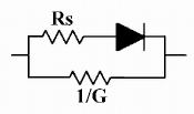
Then, a more accurate model for the stationary I–V characteristic of the diode can be formulated introducing a series resistance , accounting for the ohmic voltage drop across the semiconductor bulk, and a parallel resistance , accounting for alternative paths: Fig. (1) shows the equivalent electrical circuit; this model has four parameters, and eq. (1) modifies into:
| (4) |
Where is the current flowing into the junction, and is the current flowing into the parallel resistance; a similar modeling has been proposed in ref. Mika . Parallel and series resistances are normally introduced in the modelization of the photovoltaic cells and in the evaluation of its performance, so that the comparison of this model to the experimental data of a diode is also valuable as an introduction to the parametrization of the photovoltaic devices. A good discussion of the state of the art of the applied numerical methods is found in a recent paperHansen .
III Experimental
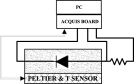
A small (4 4 4 cm3) brass cube is placed between two 30 W thermoelectric power sources/sinks assembled with commercial Peltier modules. It hosts both the device being tested, a commercial 1N4148 silicon p-n diode, and a calibrated thermistor. The direction of the heat flux can be selected through the polarity of the electric power supply connected to the modules. The heat exchanged is regulated through the duration of the power pulse in proportion to the difference between the requested temperature and the temperature registered by the thermistor. The system stabilizes the temperature of the central volume of the cube in a few tens of seconds to the value set by the operator in the range 10-100 ∘C with an accuracy better than 1 ∘C. The I–V characteristic is then measured with two differential channels of a National Instruments NI6221 data acquisition board equipped with multiplexed 16-bit ADC with selectable bipolar full scales. One of the ADC channels samples the voltage across the electrodes of the diode with a resolution of 0.3 mV and the other channel senses the current crossing the diode by measuring the potential drop on a calibrated resistor in series with the diode, with a nominal resolution of 0.02 A. is varied applying to the series diode- the variable signal of a digital-to-analog channel (DAC) of the NI6221 board. The control of the thermal cycle and of the data taking is programmed devising a LabVIEW virtual instrument. Initially, a set of temperatures is selected by the operator. After this, the controlled thermal cycles operate until the value of each is stable into a few tenths of ∘C. The couples [V,I] are saved in a file and are labelled with the temperature measured just before and just after the voltage scan. The difference of two readings of the temperature is ever less than 0.5 ∘C in absolute value, the sign being dependent on the direction of the last heat flux cycle. Thereby, we can evaluate that the value of the diode temperature is known with a precision of 0.2 ∘C on average.
IV Results and Discussion
IV.1 Shockley model
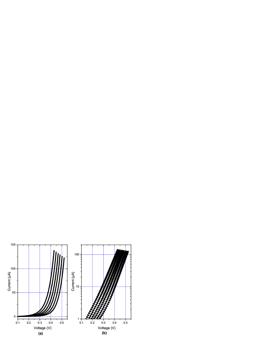
Fig. 3 shows a set of I–V curves taken at different temperatures, plotted both on linear and logarithmic scale: it is evident in the right panel the alignment of the experimental points, which is so much better for the higher temperatures and at the higher value of . The entire set of data required a time of less than ten minutes so that the measurements could be made in a standard lab session of 2-3 hours leaving time for a preliminary data analysis and a possible reiteration of the data collection.
The linearity of the experimental I–V characteristic in the logarithmic current scale reported in Fig. 3b indicates, at a glance, the region where an exponential dependence of on is likely. A first analysis of data can be done by using eq. (1), limiting the measurements to the region of moderate injection current where is dominated by diffusion. Consequently, we can neglect non-linear effects on the current, reducing the number of parameters to the two appearing in eq. (1).
We write the eq. (1) in the more compact form:
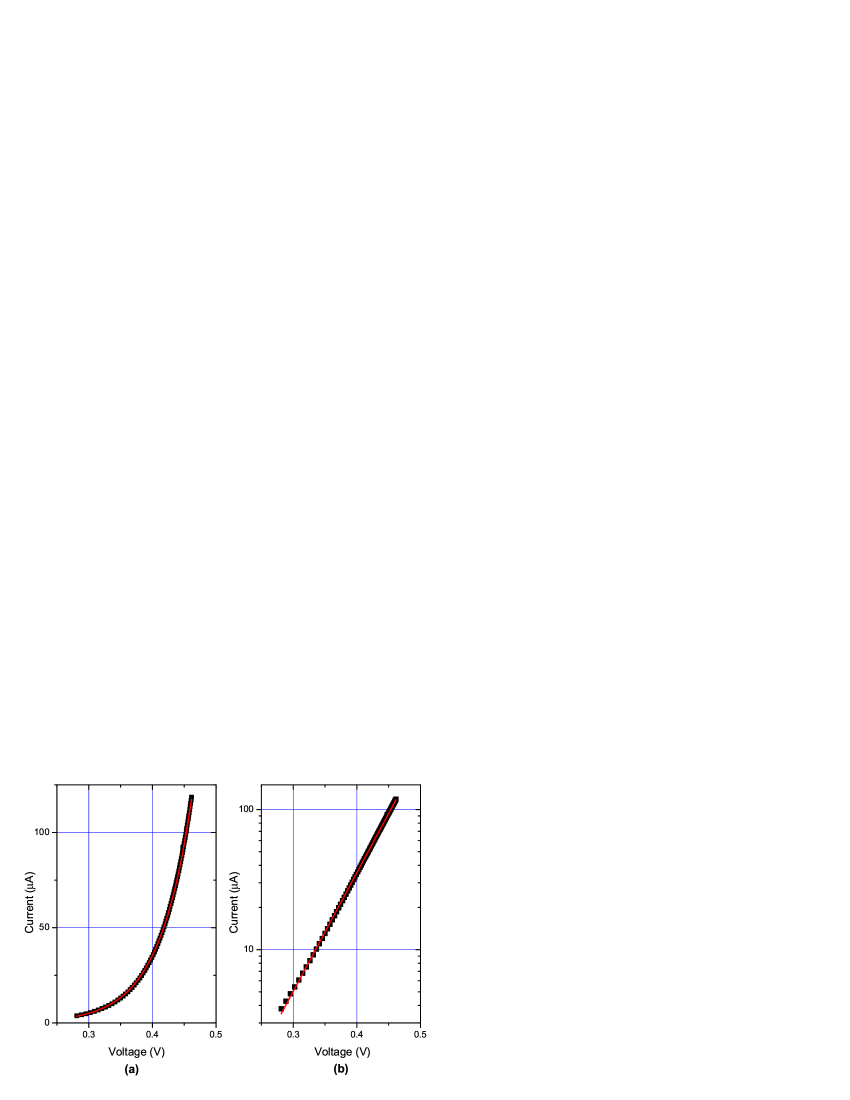
where . Fig. 4a shows a non linear fit of this equation, through a standard least square routineMatlab , which gives a value of , largely different from the ideal diode constant at the same temperature - . The agreement of the model with the data requires a value:
which is lower than the value of the SPICE models for 1N4148NXP diode but agrees with other experiments Su , pointing out the variability of this parameter due to constructive tolerance or data analysis.
A different treatment of data, often encountered in literature, considers the large value of the product in the range investigated. In this case, one can neglect the term -1 in the parenthesis and can take the natural logarithm of the measured current, finding:
The linear fit of the logarithm of the data gives with the current expressed in A and (see Fig. 4b). The differences between these values and those obtained with the complete equation are rather small, confirming the feasibility of this common and straightforward processing of data, even if a simple analysis of residuals of the two models shows that the linearized one is less accurate in the full range investigated.
IV.2 Deviations from the Shockley model
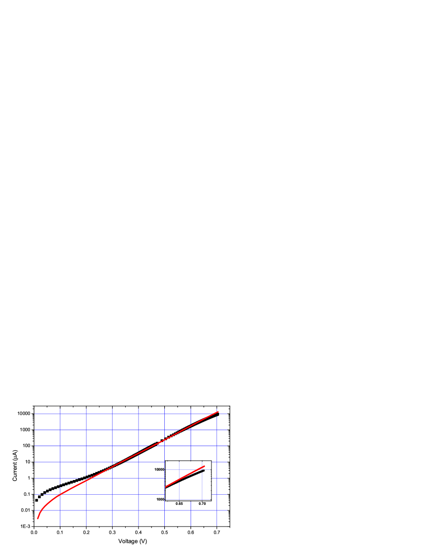
Fig.(5) shows the plot of vs. for a larger range of . The curve superimposed to the experimental data is the best fit obtained with the eq. (1), and it is evident that the two parameters model systematically underestimates lower values of the current and overestimates its higher values. A more realistic comprehension of the nature of the different contributions to the diode current, therefore, requires a study of these limiting regimes.
As explained above, besides the two parameters of the Shockley equation and , two supplementary parameters must be taken into account: and .
If the series resistance is neglected, eq. (4) simplifies into:
| (5) |
with and being the current and the voltage sensed at the diode leads, as before.
In ref. Mika the authors declare the unsuitability of the analysis of the forward I–V curve to find and suggest the extraction of this parameter through a graphical treatment of the reverse biased diode characteristic. Indeed, for the linear approximation of the exponential brings a linear relation between the current and the voltage:
| (6) |
which is not useful to calculate unless and are known or if the second term of the function of eq. (6) is negligible, as in this case (). As a matter of fact, we find it suitable to apply the same least square nonlinear fitting routine using eq. (5) as the model equation. As the first term gives an appreciable contribution only at very low values of we limit the experimental data up to a guess threshold current . The value of the small signal conductance can be determined executing the corresponding numerical fit with three parameters, , and .
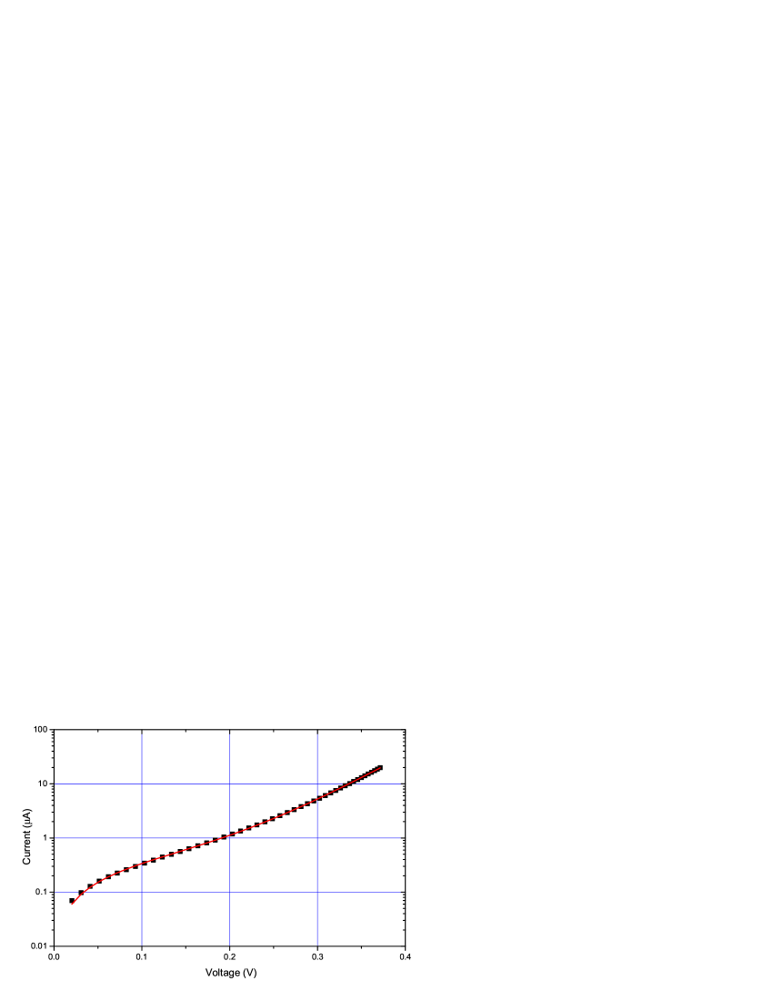
The result of the fitting procedure are shown graphically in Fig. (6) and the found values for parameters are reported in the caption. It is worth noting that and values are not in accordance with those extracted with the minimal model in the central range of the currents. This confirms that the calculated ideality factor depends on the part of the I–V curve used in its evaluation.
At the higher values of the diode current, the series resistance becomes important, while the admittance gives a negligible contribution. We may then rewrite eq. (4) as:
| (7) |
and it can be used as a fit model for the I–V data at higher currents, giving the best values of the three parameters , and . The result is shown in Fig. (7), and the found values for parameters are reported in the caption.
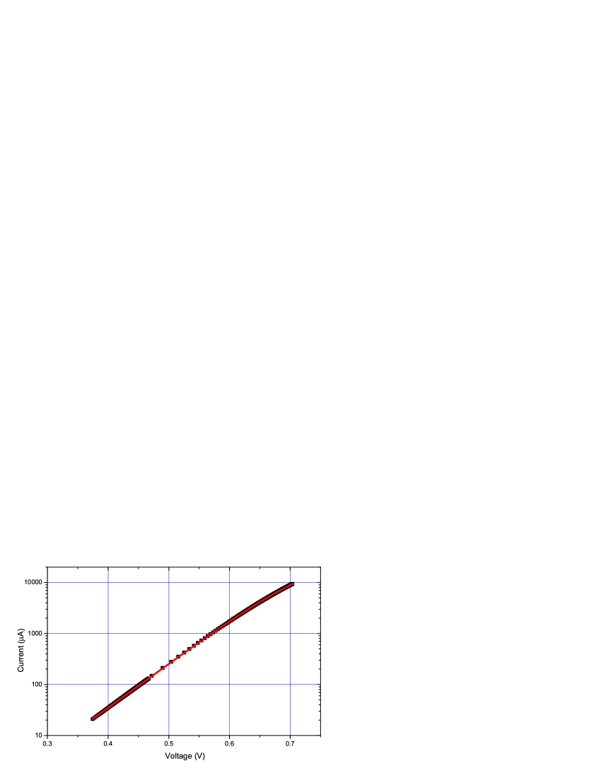
The values of the parameter are approximately coincident, by few percent, in the two parts of the curve and the coincidence is maintened by varying the value of . The values of the saturation currents differ by the order of ten percent, and the agreement is better for higher temperatures. The value of is comparable with other measurements found in literature Omar , although there the data is rather different from different sources (e.g. NXP ). We were not able to find a reliable value of for the 1N4148 diode in the literature.
IV.3 Single iterative fitting procedure
The analysis presented in the previous paragraph clearly shows that the first term of eq. 4 is significant only in the very low current region (see Fig. (6)), while at higher currents the exponential term dominates and the second term alone is able to describe the experimental data well (see Fig. (7)). This physical argument is the starting point of a numerical procedure which allows us to consider all the data together, using an iterative calculation.
We point out that by substituting in the argument of the exponential of eq. 4, an equation could be written as the objective function of a fitting procedure suitable for models expressed in an implicit form. Nevertheless, this kind of algorithms is very complex and frequently suffer from numerical instabilities.
Here we describe an alternative method, based on an iterative fitting procedure for models expressed in an explicit form, leading to the simultaneous determination of four parameters necessary to reproduce the DC diode characteristic in a large region of currents. This method can be summarized in a few steps, including the iteration described in the loop section, where is the flowing index, , and are respectively the experiment values, computed values and computed junction values of the current:
-
1
The first few data at very low currents are used to compute a first guess () of the parallel conductance with a linear fit of the model .
-
2
BEGIN LOOP Computing gives the estimate of the junction current.
-
3
The explicit model of eq. (7) is fitted with the data calculated at step 2 and the estimate of , and is found.
-
4
Updated values of the junction current are found solving numerically eq. (7) with the measured and assuming the estimate of the three parameters , and .
-
5
Updated values of total current are computed as .
-
6
The first few data of are compared to to obtain the new value : , .
-
8
END LOOP The four parameters with index are compared to previous values: if the change is much less than the estimate of their errors the loop ends, otherwise it continues, returning to step 2.
After a few iterations the four parameters converge toward stable values and the procedure may be stopped. The final result is shown in the Fig. (8) where the agreement of the model with the experimental data is very good over the entire range.
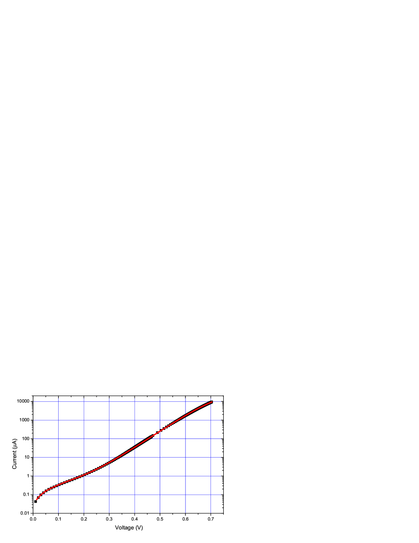
Table 1 shows the extracted parameters with the different models presented, using data of a specific current region when needed. The last set is obtained by using the iterative fitting procedure.
| G (S) | (nA) | B (V-1) | n | ||
|---|---|---|---|---|---|
| Minimal model | - | - | 14.63 (0.16) | 19.48 (0.03) | 1.856 |
| Low (eq. (5)) | 2.75 (0.01) | - | 9.72 (0.17) | 20.30 (0.05) | 1.783 |
| High (eq. (7)) | - | 2.32 (0.03) | 13.4 (0.12) | 19.78 (0.02) | 1.830 |
| Full curve (eq. (4)) | 2.80 (0.05) | 2.75 (0.05) | 10.5 (0.2) | 20.2 (0.1) | 1.790 |
IV.4 Determination of energy band gap from temperature dependence of parameters
In this section we extract energy band gap from temperature dependence of parameter, fitting I–V data taken at temperature between 10 and 100 ∘C. is not explicitly present in the Shockley equation as it is enclosed only in the saturation current ; a more detailed expression of eq. (3) is given by:
| (8) |
where depends on the geometry of the junction and the doping densities in the device.
There are two counteracting effects of an increase of on the diode current. An increase of causes a decrease of the current in eq. (1) the other parameters being fixed but, on the other hand, the same increase determines an increase of , at a given temperature. Because of the larger value of with respect to the voltage across the junction, the effect on prevails and at fixed parameters, an increase of entails an increase of .
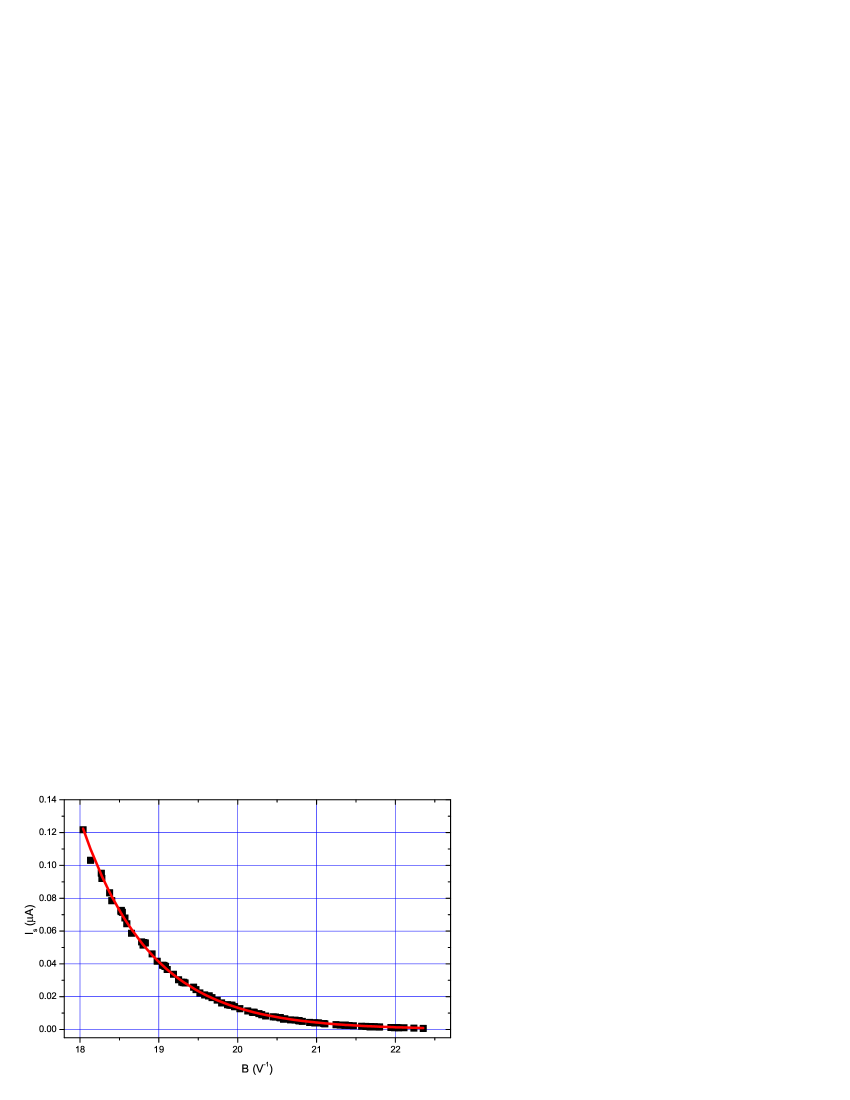
The need to consider the factor in the exponential in eq. (8) can be justified by our data, by tracing the graph of as a function of temperature, as determined by the exponential fit. The result is shown in Fig. (9) where a large set of curves I–V, taken in a two hour period, are analysed. The weak power dependence on can be neglected with respect to the exponential and the fit of the data is performed with the simplified model:
keeping the parameter defined above in the place of and expressing in . With this position the resulting parameters are and .
Other experiments using different data processing methods on Si p-n junction assert a close agreement with the accepted band-gap value of 1.12 eV at 300 K. For example, Coll report a value of 1.13 0.02 eV, operating with the base-emitter junction of a Si bipolar transistor (2N3645 model), in the temperature interval . It is not easy to find fabrication details of the 1N4148 diode and particularly information on the doping levels. Based exclusively on Orvis , the 1N4148 is fabricated by growing a slightly doped () Si micro-metric layer onto an heavily doped substrate at dopant concentration of . On the other side of -layer an acceptor dopant is then diffused forming a layer with doping density of . With these levels of dopant a band-gap narrowing of several tens of meV is predicted and observed Lanyon and could conveniently be taken into account to adjust the expected value of .
Our determination of is based on an approximate model but conceivably the factor in the relation should be considered. It is easy to understand that as this factor increases with temperature, the simplified model underestimates diode current at higher temperatures and the characteristic constants of the exponential in function of lowers with respect to the value calculated without the exponential model:
We take , which is the common choice for many different diodes, and the best fit gives the value of 1.040 0.005 eV for . The best fit value results . The two parameters are strongly correlated so that an overestimation of the exponential characteristic constant involves an underestimation of the factor and the value is 80 meV lower than the one expected and with the disposable literature data Dhari . This could be explained in terms of a high doping level at to x .
IV.5 Determination of the band gap from V–T data
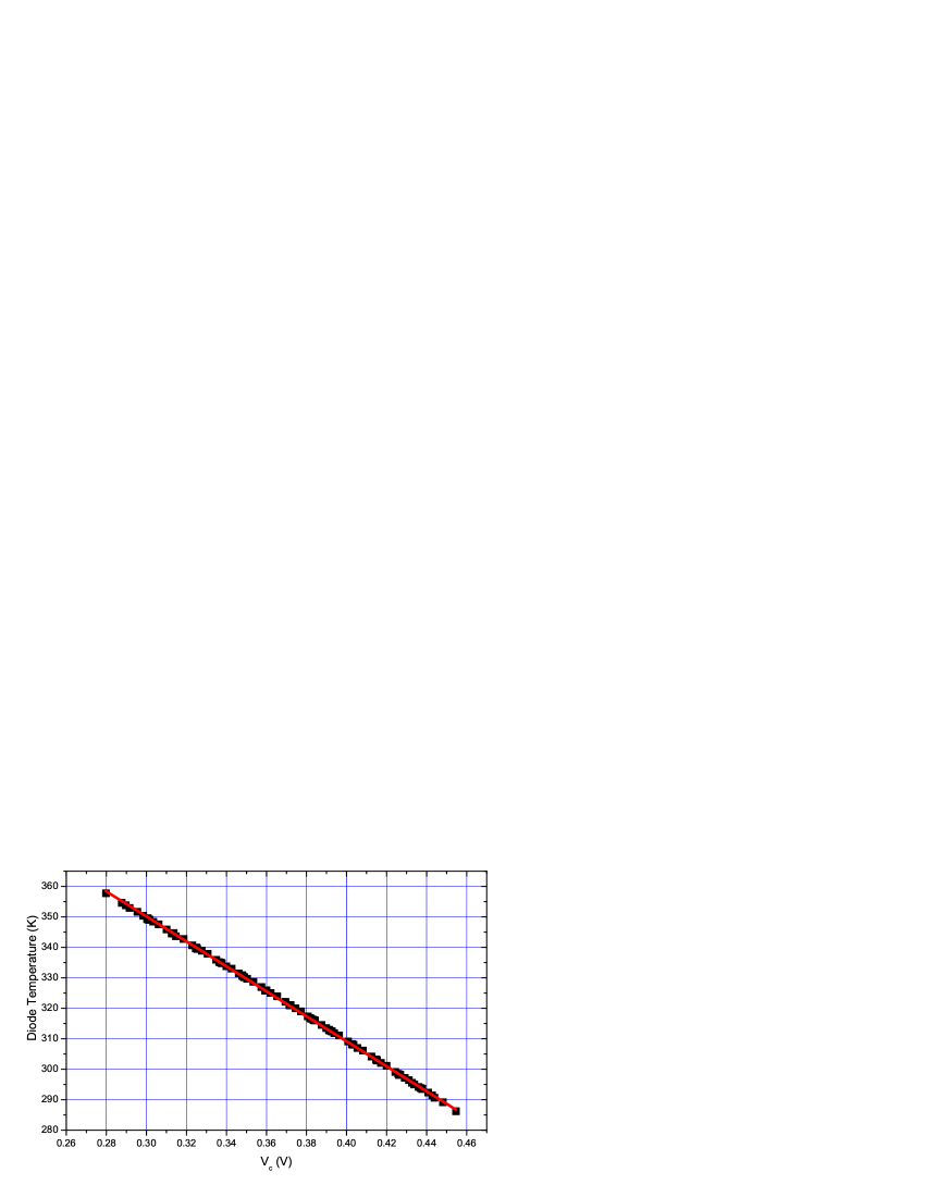
For the evaluation of the energy band-gap, a different experimental procedure is more frequently followed (and also data analysis), consisting in the recording of at different temperatures at a fixed current . It is possible to extract from our set of I–V curves the pairs at fixed diode current . The data processing consists in a linear interpolation of the value of between adjacent experimental pairs and with .
It is customary to choose in a region where the Shockley characteristic curve can be approximated by
Taking the logarithm of both sides, a linear relation is obtained:
| (9) |
with
and
so that with a simple linear fit the best values of and are calculated and:
where the possible dependencies of and cancel each other out. The final result of this analysis is shown in Fig.(10) where the linearity of is corroborated and the best fit values give eV for . The values do not depend significantly on the choice of in the region of moderate currents.
The overestimation of the expected value of is quite common in experiments driven at constant current and based on the analysis of the dependence. For example, Fischer reports a value of 1.18 0.02 eV at 300 K for the 1N4007 Si diode and Precker2 a value of 1.23 eV for the 1N4181. A good agreement with the accepted values of extrapolated at 0 K is reported by Canivez which reports 1.19 0.02 eV for the base emitter junction in a 2N2222 transistor and Kirkup (1.165 0.002 eV) in a 2N930 transistor. Finally, in Ocaya2 the authors analyze the data of a diode 1N4148, taken at different values of with a reciprocal procedure that extracts the temperature dependence of the saturation current. Assuming a pure exponential model for they find a value eV in very good agreement with the result found with our first method.
V Conclusion
We have presented a detailed analysis of the direct current-voltage characteristic of a silicon diode 1N4148. A simple numerical method, based on the standard non linear fitting algorithms used by MatLab or Octave languages, is used with models of increasing complexity. The entire procedure of measurement and modelling can be easily automated integrating the data collection performed in a LabVIEW environment with suitable numerical packages. The methodology used is relatively simple, and is suitable for an undergraduate science and engineering laboratory. The four parameters of the modified Shockley, represented in eq.(7), are extracted and their values are found in quite good agreement with the literature.
The uncertainty analysis suggests that the accuracy of the approach presented here is comparable with other methods, and it is derived mainly from theoretical model than the statistical uncertainties, defect common to the majority of methods based on I–V analysis and adopted in the current scientific and educational literature.
The advantages of the method presented here rely on the possibility to extract model parameters from data collected on a large span of values, and to easily compare simpler models, normally adopted in undergraduate laboratories.
Moreover, this analysis allows us to extract a value for within a few per cent in accordance with the accepted one, and the method is much more simple than the spectroscopic techniques which, furthermore, are also very difficult to be applied in a laboratory course. Finally, we showed that different methods of analysis of the data bring results which do not coincide with the expected one and are sometimes inconsistent. From an educational point of view, this is valuable as it warns the student against the pitfalls hidden in the choice of the fit procedures even with the same model and the same data.
References
References
- (1) C. Zhang et al., “A simple and efficient solar cell parameter extraction method from a single current-voltage curve”, J. Appl. Phys., vol. 110, pp. 064504, 2011
- (2) M. Barkelid, V. Zwiller, “Single carbon nanotube photovoltaic device”, J. Appl. Phys., vol. 114, pp. 164320, 2013
- (3) R.E. Thorne, “A history of the I-V characteristic of CDW conductors”, J. Phys., vol 131, pp. 89–94, 2005.
- (4) D. Johnston and S. Miai-Sin Wu, Foundations of cellular neurophysiology, Cambridge, MA: MIT Press, 1995. See Chapter 3 for an elementary introduction to the topic.
- (5) H.W. Fink, C. Schonenberger, “Electrical conduction through DNA molecules”, Nature, vol. 110, pp.407, 1999
- (6) Kathleen Meehan, ”Explaining semiconductor device physics with a fusion of lectures and videos”, Frontiers in Education Conference, 2013 IEEE. IEEE, 2013.
- (7) G.W. Neudeck, The PN junction diode. 2 edition, Reading MA: Addison-Wesley, 1989.
- (8) F.E. Inman, C.E. Miller, “The Measurement of e/k in the Introductory Physics Laboratory”, Am. J. Phys, vol. 41, pp. 471-473 Mar.1973
- (9) I. Martil and G. Gonzalez Diaz, “A laboratory experiment for DC characterization of p-n device”, Eur. J. Phys., vol. 12, pp. 149-152, 1991
- (10) Y. Canivez, “Quick and easy measurement of the band gap in semiconductors”, Eur. J. Phys., vol. 4, pp. 42-44, 1983
- (11) J.W. Precker,“Simple experimental verification of the relation between the band-gap energy and the energy of photons emitted by LEDs”, Eur. J. Phys., vol. 28, pp. 493, 2007
- (12) S. Chand and J. Kumar, “Current-voltage characteristics and barrier parameters of Pd2Si/p-Si (111) Schottky diodes in a wide temperature range”, Semicond.Sci.Tech, vol 10, pp.1680-1688, 1995
- (13) A. Kaminski, J.J. Marchand, and A. Laugier, “I–V methods to extract junction parameters with special emphasis on low series resistance”, Solid-State Electronics, vol 43 pp.741-745, Apr. 1999.
- (14) V. Mikhelashvili, G. Eisenstein, V. Garber, S. Fainleib, G. Bahir, D. Ritter, M. Orenstein and A. Peer, “On the extraction of linear and nonlinear physical parameters in nonideal diodes.” J. Appl. Phys., vol. 85, pp. 6873-6883, May 1999.
- (15) C.W. Hansen, “Estimation of Parameters for Single Diode Models Using Measured IV Curves”, 39th IEEE Photovoltaic Specialists Conference, Tampa, FL. 2013.
- (16) Consider for reference the functions fitnonlin of the MatLab libraries or leasqrdemo of the Octave packages.
- (17) The SPICE model published by NXP Semiconductors reports a value n = 1.906 (see http://www.nxp.com/documents/spice_model/1N4148.prm, last accessed 7 January 2016).
- (18) H-H. Su, C.W. Kuo and T. Kitazawa, “A novel approach for modelling diodes into FDTD method” PIERS Proceedings., pp. 20-23 Mar. 2011.
- (19) N.I.C. Omar, N.F. Hasbullah, N.K.A.M. Rashid and J. Abdullah, “Electrical properties of neutron-irradiated silicon and GaAs commercial diodes”, 2012 IEEE Symposium on Industrial Electronics and Applications (ISIEA), pp. 90-94, IEEE, Sep. 2012.
- (20) P.J. Collings, “Simple measurement of the band gap in silicon and germanium”, Am. J. Phys, vol. 48, pp. 197-1999, Aug.1980.
- (21) W.J. Orvis, G.H. Khanaka, and J.H. Yee,“Development of a GaAs solid state device model for high power applications”, Electrical Overstress– Electrostatic Discharge Symposium Proceedings, 1987. ESD Association, 1987.
- (22) H.P.D. Lanyon and R.A. Tuft, “Bandgap narrowing in moderately to heavily doped silicon”, IEEE Trans.Elec.Dev., vol 26, pp. 1014-1028, 1979.
- (23) S.R. Dhariwal and V.N. Ojha, “Some simple observations on the bandgap narrowing in heavily doped silicon”, Sol.St.Elect., vol. 28, pp. 845-846, 1985
- (24) C.W. Fischer, “Elementary technique to measure the energy band gap and diffusion potential of pn junctions”, Am. J. Phys, vol.50, pp. 1103-1105, Dec. 1982.
- (25) J.W. Precker and M.A. da Silva, “Experimental estimation of the band gap in silicon and germanium from the temperature–voltage curve of diode thermometers”, Am.J.Phys., vol. 70, pp. 1150-1153, Nov. 2002.
- (26) L. Kirkup and F. Placido, “Undergraduate experiment: Determination of the band gap in germanium and silicon”, Am.J.Phys., vol. 54, pp. 918-920, Oct. 1986.
- (27) R.O. Ocaya and F.B. Dejene, “Estimating p–n diode bulk parameters, bandgap energy and absolute zero by a simple experiment”, Eur. J. Phys., vol. 28, pp. 85-91, Jan.2007.