The Conversion of CESR to Operate as the Test Accelerator, CesrTA, Part 4: Superconducting Wiggler Diagnostics
Abstract
Cornell’s electron/positron storage ring (CESR) was modified over a series of accelerator shutdowns beginning in May 2008, which substantially improves its capability for research and development for particle accelerators. CESR’s energy span from 1.8 to 5.6 GeV with both electrons and positrons makes it appropriate for the study of a wide spectrum of accelerator physics issues and instrumentation related to present light sources and future lepton damping rings. Additionally a number of these are also relevant for the beam physics of proton accelerators. This paper, the last in a series of four, describes the vacuum system modifications of the superconducting wigglers to accommodate the diagnostic instrumentation for the study of electron cloud (EC) behavior within wigglers. Earlier papers provided an overview of the accelerator physics program, the general modifications of CESR, the modifications of the vacuum system necessary for the conversion of CESR to the test accelerator, CESRTA, enhanced to study such subjects as low emittance tuning methods, EC effects, intra-beam scattering, fast ion instabilities as well as general improvements to beam instrumentation. While the initial studies of CESRTA focussed on questions related to the International Linear Collider damping ring design, CESR is a very versatile storage ring, capable of studying a wide range of accelerator physics and instrumentation questions.
keywords:
Accelerator Subsystems and Technologies, Beam-line Instrumentation1 Overview of CESR Modifications
The conversion of CESR to permit the execution of the CESRTA program [1] required several extensive modifications. These included significant reconfiguring of CESR’s accelerator optics by removing the CLEO high energy physics (HEP) detector and its interaction region, moving six superconducting wigglers and reconfiguring the L3 straight section[1]. There were also major vacuum system modifications to accommodate the changes in layout of the storage ring guide-field elements, to add electron cloud diagnostics and to prepare regions of the storage ring to accept beam pipes for the direct study of the electron cloud[2]. A large variety of instrumentation was also developed to support new electron cloud diagnostics, to increase the capabilities of the beam stabilizing feedback systems and the beam position monitoring system, to develop new X-ray beam size diagnostics and to increase the ability for studying beam instabilities[3]. This conversion process included the development of special instrumentation for the study of EC within superconducting wigglers and these are described in the following section. The entire conversion occurred in down periods over several years, during which the operation of the Cornell High Energy Synchrotron Source (CHESS) was maintained for synchrotron x-ray users.
1.1 Motivation for CESR Modifications
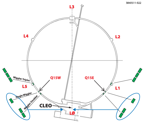
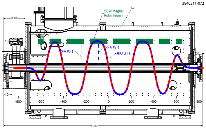
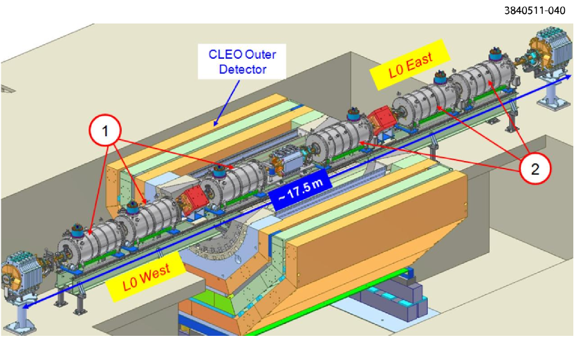
CESR’s vacuum system is an essential part of its accelerator beam transport system, which is capable of storing total electron and positron beam currents up to 500 mA (or single beam up to 250 mA) at a beam energy of 5.3 GeV. As shown in Figure 1 the CESR vacuum system with a total length of 768.44 m consists primarily of bending chambers in the arcs, two long straight sections, called (18.01 m in length) and (17.94 m in length), and four medium length straights (called and both 8.39 m in length and and both 7.29 m in length).
In the CESR-c/CLEO-c era 12 home-built superconducting wigglers (SCWs) were installed in CESR[4], with two triplets at and , two doublets and two singlet SCWs in the arcs (see Figure 1). This complement of SCWs plays an important role in the CESRTA program[1, 2, 3]. These SCWs additionally represent a good model for the wigglers planned for the International Linear Collider (ILC) damping rings[5]. At the conclusion of CLEO-c HEP program in March 2008, staged modifications were carried out to convert CESR into the test accelerator CESRTA [1, 2, 3]. The motivation for the vacuum system modification was to support the physics programs of CESRTA, including: (1) Ultra-low emittance lattice design, tuning and associated beam instrumentations, and (2) Electron cloud studies, including the development and verification of suppression techniques for ECs.
During the reconfiguration of L0, including the removal of the central part of the CLEO HEP Detector and the IR vacuum chambers, 6 SCWs [4 CESR-c and two CESRTA SCWs, equipped with retarding field analyzers (RFA)] were installed along with many new chambers containing additional EC diagnostics, such as RFAs and beam position monitor (BPM)/TE-wave buttons.
2 Wiggler Chambers
2.1 Design Considerations for Wiggler RFA Structure
Superconducting wigglers (SCWs) were designed and fabricated for the CESR-c/CLEO-c program. The CESR-c wigglers are 8-pole super-ferric magnets with the main period of 40 cm and trimming end poles. The SCWs provide a very uniform transverse field up to 2.1 T, closely matching the ILC DR wiggler requirements. Therefore, these SCWs are ideal test vehicles for the study of EC growth and suppression in the wiggler field. With this motivation a thin-style RFA design was developed for the wiggler beam pipe and a set of diagnostic chambers was constructed by a collaboration including Cornell, KEK, LBNL and SLAC.
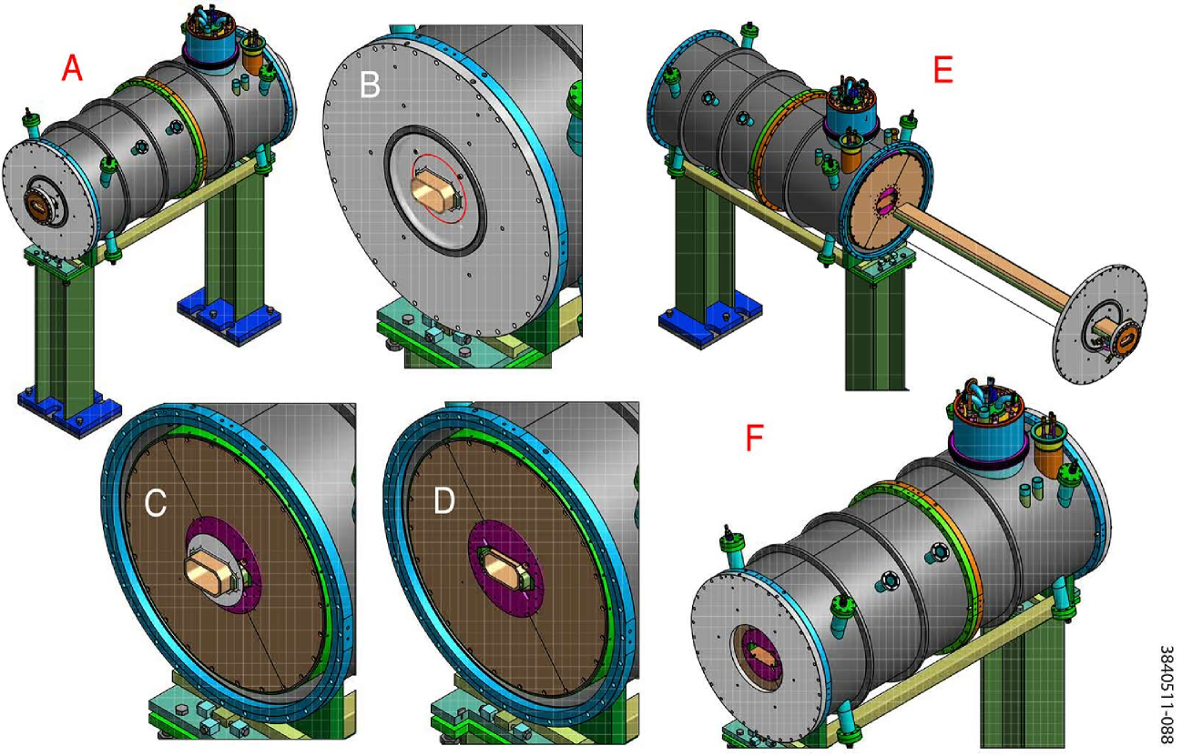
Figure 2 illustrates the structure of the SCW. The details regarding the design of the CESR-c SCWs can be found in [4]. In the original SCW production, the beam pipe was assembled into the magnet’s cold-mass and the cold-mass with the beam pipe was in turn inserted in the isolation vacuum vessel. Sixteen SCWs were constructed for the CESR-c program on a specially designed SCW assembly line in a dedicated facility that no longer exists. Therefore, the following design constraints were imposed on the RFA beam pipe design and construction.
-
•
The RFA beam pipe must fit inside the space in the cold-mass thermal shield (see Figure 2) while still providing sufficient beam aperture.
-
•
The removal of the existing beam pipe and the insertion of the RFA beam pipe must be accomplished without disassembling or disturbing the wiggler magnet structure.
-
•
The RFA beam pipe (including all material used) must be UHV-compatible.
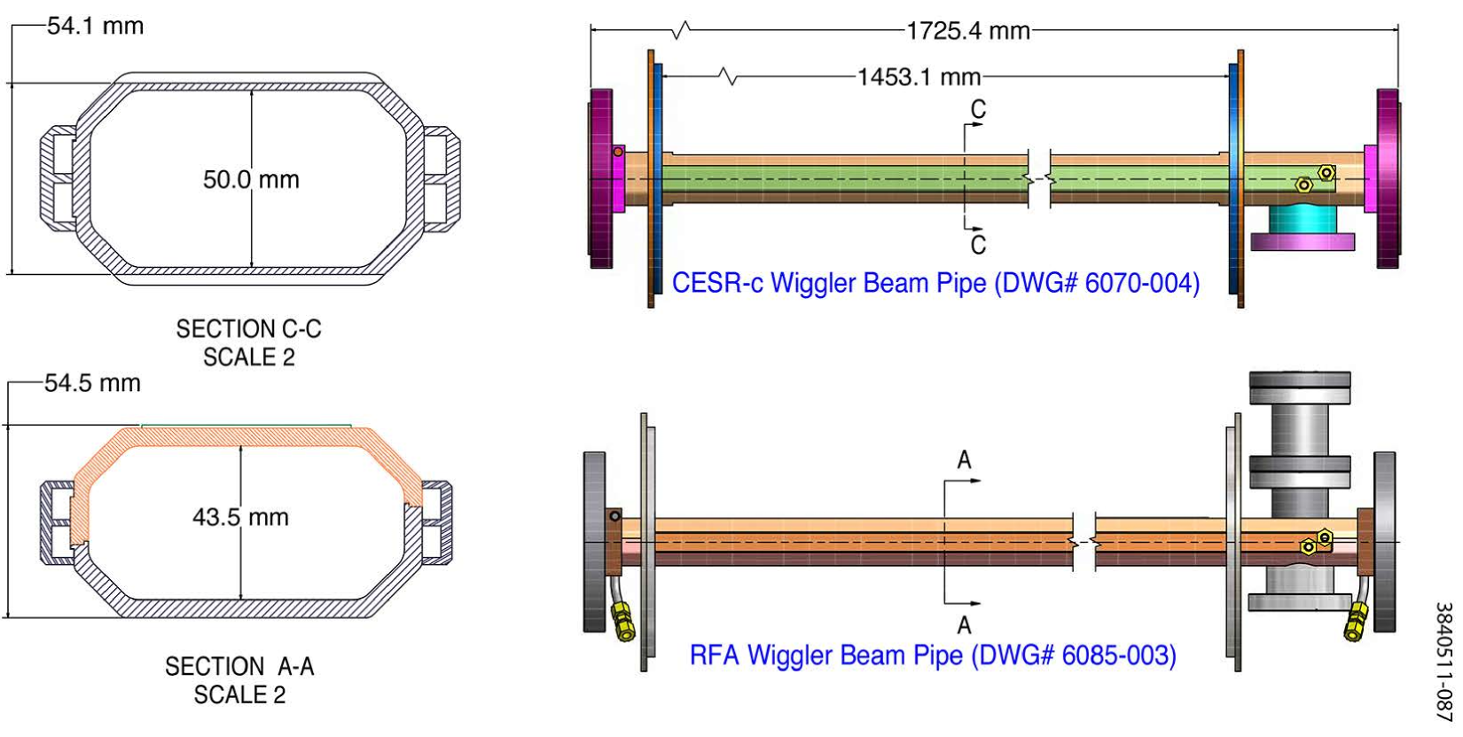
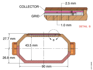
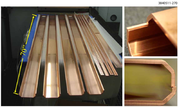
With these requirements the vertical aperture of the RFA beam pipe was reduced from the standard 50 mm to 43.5 mm to provide space for the RFAs, as shown in Figure 3. The copper extrusions were split into top and bottom halves. After trimming the vertical edges, the two halves were re-joined (via electron beam welds) to form the RFA beam pipe.
Over the first three years, four SCWs equipped with RFA beam pipes, were constructed and installed for the CESRTA program [1, 2, 3]. The next five sections describe this process for implementing RFAs in the superconducting wiggler magnets in some detail. This is to provide adequate documentation to support the integrity of the instrumentation and to address concerns, which might call the measurements into question. They also provide guidance for any future developments of wiggler-based RFAs. Lastly, these sections allow enough details for future simulations of EC development in these SCWs.
Of the first two units, one has a bare copper beam pipe and the other has a copper beam pipe coated with a TiN thin film (prepared by the SLAC team.) In the third and fourth units, a grooved plate and an EC clearing electrode were implemented on the bottom half of the beam pipe. Details for these four assemblies are found in the following sections.
2.2 Overview of RFA Construction
As detailed later in this section, the top half beam pipe houses the RFA assemblies, while a variety of EC suppression techniques were implemented on the bottom half beam pipe. The experimental program for the wiggler vacuum chamber mitigation studies occurred as summarized below.
-
•
A bare copper chamber installed for a reference SCW measurements in October 2008.
-
•
Copper chamber coated with TiN also installed in October 2008.
-
•
Grooved SCW chamber placed in CESR in July 2009 and operated in experimental runs (July 2009 to September 2009, and November 2009 to December 2009) and two CHESS runs (September 2009 to November 2009, and January 2010 to March 2010.)
-
•
In the April 2010 CESR shutdown, the preceding SCW assembly was replaced with a SCW vacuum chamber fitted with RFA beam pipe, having an EC clearing electrode.
-
•
The grooved RFA SCW assembly was coated with TiN and then reinstalled in the L0 EC experimental region in January 2011.
Simulations [6] predicted distinct longitudinal and transverse EC density distributions in wiggler beam pipes. The design goal of the wiggler RFA beam pipe is to place RFAs at strategic longitudinal locations in the wiggler magnetic field to measure the corresponding transverse EC density distributions.
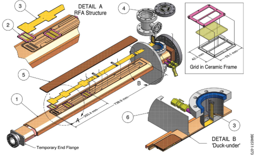
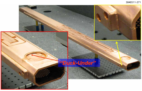
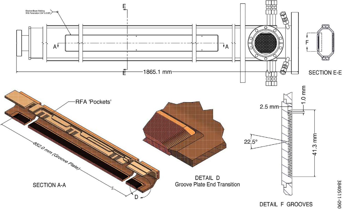
The RFA beam pipe design is illustrated in an exploded view in Figure 4. The RFA beam pipe is constructed from the top and bottom halves of the same extrusions as used for original SCW beampipes. Along the longitudinal direction of the beam pipe, three pockets were machined into the top half of the beam pipe to form housings for the three RFAs. The three RFAs’ locations together with the vertical field map of the SCW are depicted in Figure 5. After installation in the wiggler magnet, the RFA #1 is at boundary between two center poles (zero vertical magnetic field), #2 at center of a pole (maximum vertical magnetic field) and #3 at ‘edge’ of a pole (longitudinal B-field).
Electrons from the EC in the beam pipe pass through transmission holes to the RFA detector. There are 240 small holes in each of the three RFAs. As shown in Figure 6, they are grouped into 12 segments in the transverse direction to the beam pipe. These holes have a diameter of 0.75 mm ( of the wall thickness) to reduce noise from the beam’s radio frequency (RF) electromagnetic interference (EMI.)
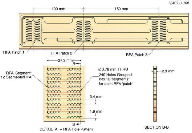
The retarding grids are nested in ceramic frames with the frames bolted to the RFA housing pockets. Two generations of metallic meshes were used as the retarding grids. The first generation was made of photo-chemically etched 0.15 mm-thick stainless steel (SST) mesh, with an optical transparency of approximately 38%. The SST mesh is easy to handle and inexpensive. However, the SST mesh has two drawbacks. Its relatively low transmission not only directly translates to low EC detection efficiency, but also limits the EC diagnostic accuracy due to significant interaction of the transmitted electrons with the grid. To reduce the secondary emission from the grid, the SST meshes were coated with approximately 0.3 m of gold. The second generation grids (by Precision EForming, Inc) were electro-formed copper meshes, bonded to SST frames (supplied by Cornell). The electro-formed copper meshes were also coated with gold (approximately 0.3 m in thickness) via electroplating to reduce secondary electron emission. The electro-formed meshes consist of 15 m wide and13 m thick copper wires with spacing 0.34 mm in both transverse directions and an optical transparency of approximately 92%. The disadvantage of the copper electro-formed mesh is that it is very expensive and fragile.
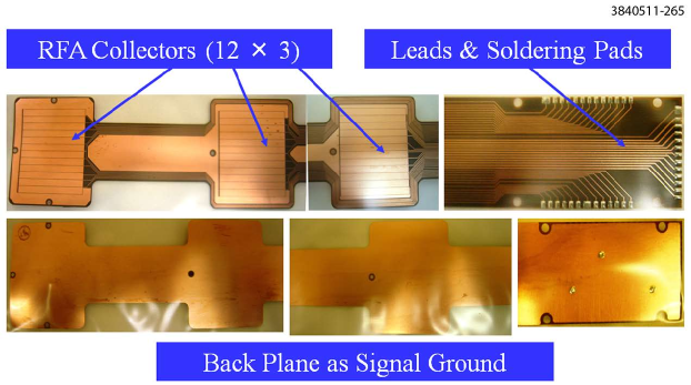
Similar to the thin RFA design[7], a flexible copper-clad/Kapton circuit was used as RFA electron collector. As shown in Figure 7, three sets of RFA pads each contain 12 transverse collectors to match the hole patterns on the RFA beam pipe. After tinning the soldering pads with Sn(63%)Pb(37%) solder, the flexible circuits were cleaned and degassed with a 150∘C vacuum bakeout before insertion in the RFA beam pipe. Vacuum measurements (with a residual gas analyzer) showed acceptable vacuum properties for the clean flexible circuits. The flexible circuit strip was laid on top of the ceramic frames of the grids and precisely positioned with ceramic head-pins. After positioning the flexible circuit and feeding its connection pad through a ‘duck-under’ channel (see ‘Detail B’ in Figure 4) into the RFA connection port, ultra high vacuum- (UHV-) compatible Kapton-coated copper wires (42 wires per assembly) were soldered to the connection pads. These wires were also pre-tinned and cleaned so that the entire RFA circuit is free from solder flux. The final RFA connections are wired to three 15-pin D-type vacuum feedthroughs on a 4.5 inch ConFlat© flange. A copper RFA vacuum cover was electron-beam welded to the beam pipe’s top half to complete the RFA assembly. Figure 8 shows the cross-section of the RFA beam pipe at one of the RFA locations. The entire RFA structure is contained within a total vertical space of 2.5 mm.
2.3 Preparation of SCW for RFA Beam Pipe
Preparations must be undertaken for a CESR-c SCW to receive an RFA beam pipe assembly. The main task is to extract the existing beam pipe from a CESR-c SCW without disturbing the magnet’s structure. As shown in Figure 2, the CESR-c SCW beam pipe is attached to the insulating vacuum vessel via two thin stainless steel disks. The major portion of these disks is about 1.5 mm thick. Called flexible disks, they allow for differential thermal expansion and contraction of the beam pipe relative to the vacuum vessel. The flexible disks completed the insulation vacuum envelope after being welded to the beam pipes and the large end flanges of the vacuum vessel. The sequence of the beam pipe extraction from a CESR-c SCW is described in Figure 9. After the extraction of the beam pipe, all debris from the extraction operation was thoroughly removed from the magnet and a pair of large end flanges (with O-ring seals) were mounted to the insulation vacuum vessel. Then the vacuum vessel was leak checked. The integrity of the wiggler magnet was also verified.
2.4 RFA Beampipe Fabrication and Integration to SCW
This section describes the hardware construction and installation for and RFA in a bare copper beam pipe. Many steps of heavy welding are required as part of the RFA wiggler beam pipe construction. As illustrated in Figure 4, we have designed the equipment in a such way so as to have all the welding that may overheat the portions of the beam pipe near the RFA flexible circuit completed prior to the installation of the flexible circuit. This Kapton©-based circuit has a temperature rating of 220∘C. To address this requirement, a ‘duck-under’ channel was created beneath the stainless steel flexible disk, which later was welded to the wiggler insulation vacuum vessel. During the construction process all vacuum welds, except the final RFA vacuum cover, can be completed and leak checked prior to the installation of the heat-sensitive flexible circuit. Utilizing the ‘duck-under’ channel, one can feed the flexible circuit from the RFA portion of the beam pipe (i.e. inside wiggler insulation vacuum space) to the RFA connection port.
The beam pipe fabrication itself began by splitting the fully annealed oxygen free electronic (OFE) copper extrusion into two halves. The copper extrusions are the same type used for PEP II Low Energy Ring (LER) Quad beam pipe and the original CESR-c SCW beam pipes. All RFA-related features on the top half were machined at LBNL’s machine shop with computer numerically controlled (CNC) machinery. These include the RFA grid pockets, 720 electron transmission holes, the ‘duck-under’ channel, and all the EB weld-preps (see photos in Figure 10). After cleaning, an ‘under cover plate’ was EB welded to the top half of beam pipe to form the ‘duck-under’ channel. Then two finished halves were joined together using a CNC EB welder, with approximately a 1 mm electron-beam penetration at the seams. After passing a leak check of the beam pipe seams, two side cooling channels were then EB welded to the beam pipe (see photos in Figure 11). Measurements using numerically controlled (NC) coordinate machine found that amount of distortion of the EB-welded beam pipe is well within design tolerances. Subsequently, all other vacuum components (including end flanges and transitions, RFA connection port and vacuum pumping port) were manually welded to the beam pipes with tungsten inert gas (TIG) welding in an argon atmosphere to avoid the oxidation of the copper beam pipes. A temporary flange was welded to the end of the beam pipe, which is away from the RFA locations, to facilitate initial leak checking, bakeout and TiN coating. At this stage all the UHV joints of the beam pipes, with exception of the top RFA vacuum cover plate, were finished and the beampipe was ready for the final RFA component assembly. To ensure the required UHV quality, both beam pipes were baked to 150∘C under vacuum. After the bakeout, one of the two RFA beam pipes produced at LBNL was coated with TiN thin film on the beam pipe’s interior by the SLAC team. By comparing with the TiN coated and bare copper chambers using the CESRTA diagnostics, the effectiveness of TiN coating in suppressing EC in wiggler magnetic fields could be evaluated.
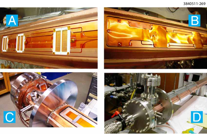
The first two partially finished wiggler beam pipes at LBNL were shipped to Cornell (in September 2008) for final RFA component assembly and integration into the SC wiggler assemblies. Photos in Figure 12 show some of the key steps of the RFA installation. The entire RFA installation was performed in a Class 1000 Clean Room. After thorough electrical checks the RFA installation was finished by E-beam welding on the OFE copper RFA vacuum cover. The finished RFA beam pipes were baked to 150∘C for 48 hours before final insertion into the prepared wiggler magnet assemblies.
Before integrating the RFA beam pipe into the SCW, the temporary flanged end (end away from the RFAs) was machined off using a clean milling machine with clean cutting tools. Extreme care was taken in this final machining step, which included blocking metallic debris from entering the RFA section of the beam pipe and constant purging of the chamber with N2. The RFA beam pipe was inserted into the wiggler warm-bore and precisely positioned with respect to the wiggler magnet by optical survey. Extreme care was also taken in the final welding stages (including final beam pipe flange and seals to the wiggler insulation vacuum vessel) to prevent overheating of the RFA components.
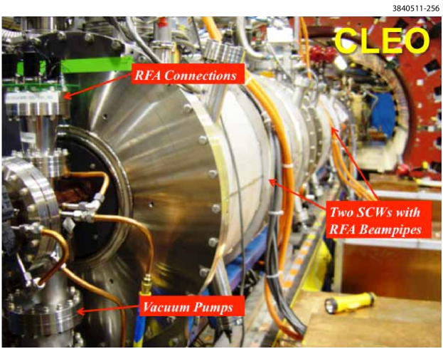
Finally, the completed SCWs with RFA beam pipes were ‘baked’ at 70∘C for 2 days by circulating hot water through the beam pipe cooling channels in an effort to de-gas the vacuum components after the prolonged air exposure during the final RFA beam pipe insertion and welding. The first two SCWs with RFA beam pipe were successfully installed in the west side of the L0 Experimental region in CESR in October 2008 (see Figure 13) in the SCW02WA and SCW02WB locations (refer to Figure 14).
2.5 Grooved Chamber
Using grooved surfaces to lower effective secondary emission yield (SEY) is a well-known [8, 9, 10, 11] passive technique to suppress EC growth in a magnet field. Having successfully implemented RFAs into SCWs in CESR, we studied the effects of grooved chambers by constructing an RFA-equipped SCW chamber with a grooved insert installed on the bottom surface. Figure 15 shows the design of the RFA beam pipe. This beam pipe assembly is basically identical to the design as shown in Figure 4 with the exception that a copper plate with triangular grooves has been attached to the bottom half via EB-welding. The same procedure (described above) was followed for the RFA installation to the beam pipe and the beam pipe integration into the SCW.
The direct implementation of a grooved surface in a copper extrusion was found to be quite challenging. Practical considerations dictated the implementation of the grooved surface using an inserted plate. First, it was determined (through test machining) that the copper extrusions used for the SCW beam pipe were fully annealed, and too soft for machining the sharp-tipped grooves. Thus the grooves were machined in a separate plate of full-hard OFHC copper which could be electron-beam welded into the vacuum chamber instead of directly being machine onto the bottom half extrusion. However, even in the case of machining a separate plate, it was too costly to machine grooves for the entire length of the chamber. Thus, for the experimental tests a grooved plate of sufficient length to span the RFAs was used.
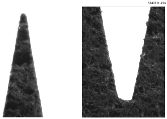
The geometry and dimensions of the grooves are shown in the ‘Detail F’ in Figure 15. A cut-out opening was machined for the grooved plate into the bottom half of the beam pipe (Figure 16). Sloped cuts of 30∘ were made on both ends of the groove plate and on the beam pipe wall (shown in ‘Detail D’ in Figure 15), which provide a smooth transition from the flat surface to the triangular groove tips in order to minimize higher order mode loss (HOML.)
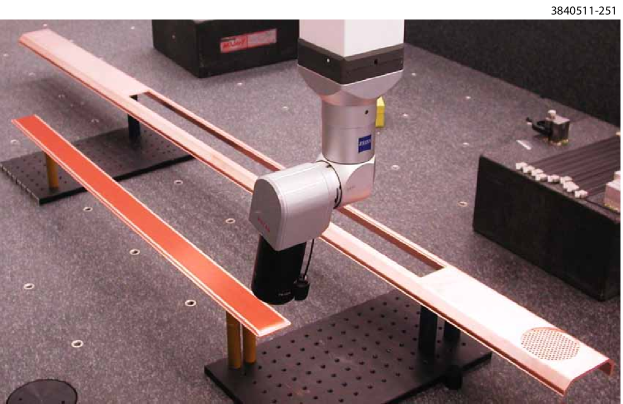
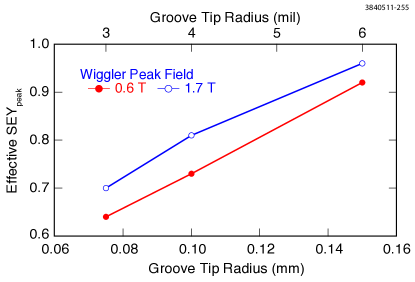
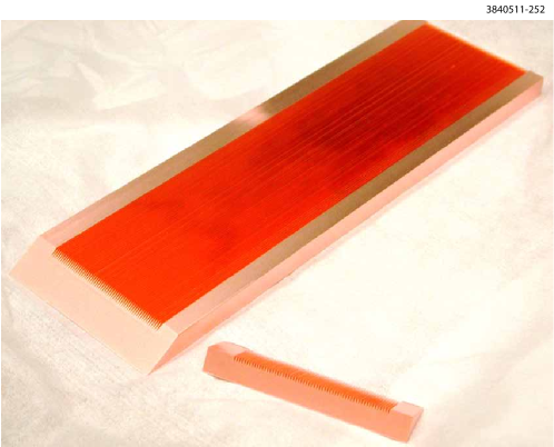
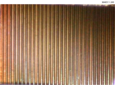
The triangular grooves were made with a milling technique using specially designed cutters. In practice there will be finite radius on the tips and valleys of these grooves. The effective peak SEY on these triangular grooves was simulated as a function of the tip/valley radius by Wang [12]. As shown in Figure 17 for the grooved surfaces to be effective in suppress SEY, it is essential to produce these triangular grooves with average radius of their tips and valleys smaller than 0.003" (75 m). To qualify this groove fabrication technique, a prototype groove plate (of same width, but 150 mm long) was produced for inspection. Figure 18 shows the prototype groove plate, and images from optical inspections. The resulted tip and valley radii were approximately 25 m and 60 m, respectively, which were satisfactory.
The RFA beam pipe assembly, having the RFA features on the top half and the grooved plate on the bottom half, was fabricated at LBNL and delivered to Cornell in May 2009. The thin RFAs were assembled into the beam pipe and then the RFA beam pipe was inserted into a SCW, following a similar procedure as describe previously in this section. Extra measures were taken to protect the sharp grooves at the bottom of the beam pipe throughout the final stages of assembly. The completed SCW was successfully installed for the CESRTA program [1, 2, 3] in the L0 EC experimental region in July 2009 in the SCW02WB location (refer to Figure 14).
 |
 |
The SCW beam pipe assembly, containing the grooves and their associated RFAs, was successfully operated through two CESRTA experimental runs (July 2009 to September 2009, and November 2009 to December 2009) and two CHESS runs (September 2009 to November 2009, and January 2010 to March 2010), accumulating total beam doses of approximately 940 Amphr. During the April 2010 CESR shutdown, this SCW assembly was replaced with a SCW assembly fitted with RFA beam pipe, having an EC clearing electrode (see the subsequent sub-section). After its removal from CESR the following procedures were performed on the grooved RFA beam pipe as a continuing effort in studying EC suppression in wigglers.
-
•
During the CHESS runs (and some of the CESRTA experimental runs), short electron/positron bunches with high bunch current were stored. Therefore, concerns were raised as to whether the high image current density on the sharp groove tips may have caused over-heating that resulted in damage. Close-up optical inspection of the grooves was carried out with a combination of a specially design ’trolley’ (that locates a mirror above the grooves in the beam pipe) and a high-zoom digital camera. The entire length of the groove plate was inspected for damage to the groove tips. No observable damage was found.
-
•
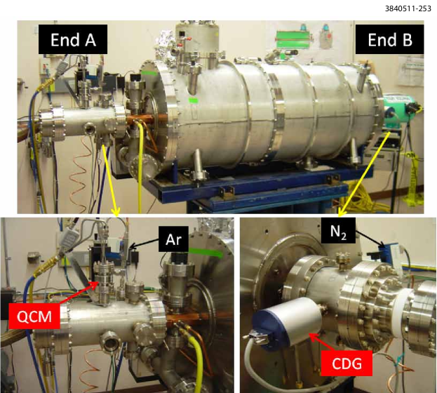
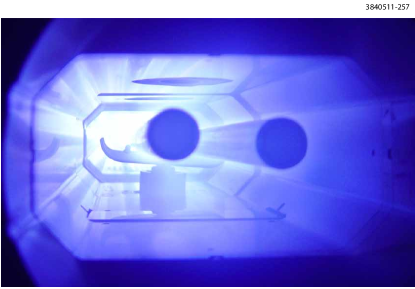
Using a DC sputtering technique, a TiN thin film coating was applied to the interior surfaces of the beam pipe, including the grooved portion at the bottom beam pipe. The coating setup is shown in Figure 19. Figure 20 displays the uniform discharge during the TiN thin film deposition. The TiN deposition was undertaken in two stages with the titanium cathodes shifted transversely to minimize the geometric shadowing of the steep grooves. The estimated TiN film thickness was 150 to 500 nm, based on the on-line measurements of a QCM (Quartz Crystal Micro-balance) and the off-line measurements of witness coupons.
-
•
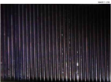
Close-up optical inspection of the grooves was done after the TiN coating. Figure 21 shows typical inspection images of a portion of the grooves before and after the TiN coating. Although the camera did not possess sufficient resolution for the fine features of the sharp tips/troughs, no obvious sign of over-heating and damage to the grooves were visible. The image also showed relatively uniform TiN coating with no significant shadowing within the groove troughs.
The TiN coating process was performed in the presence of RFA assemblies with all RFA grids and collectors grounded. The RFAs were found to be fully operational after coating in this manner. The TiN coated, grooved RFA SCW assembly was reinstalled in the L0 EC experimental region in SCW02WA location in January 2011.
 |
 |
2.6 Clearing Electrode Chamber
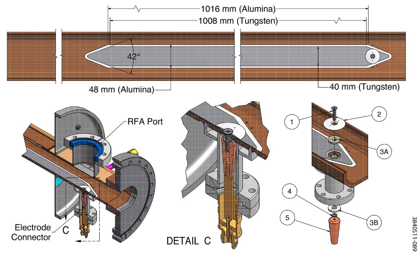
One of the electron cloud mitigation methods studied at CESRTA makes use of a clearing electrode, operating with a positive bias voltage to attract the electrons, which would ordinarily collect around the positron beam. To investigate its EC suppression efficacy in the wiggler field, a clearing electrode was installed on the bottom of an RFA-equipped beam pipe in a SCW. The structure of the beam pipe is shown in Figure 22. The beam pipe consists of a top half with three RFAs (identical to the design as shown in Figure 4) and a bottom half with a clearing electrode assembly.
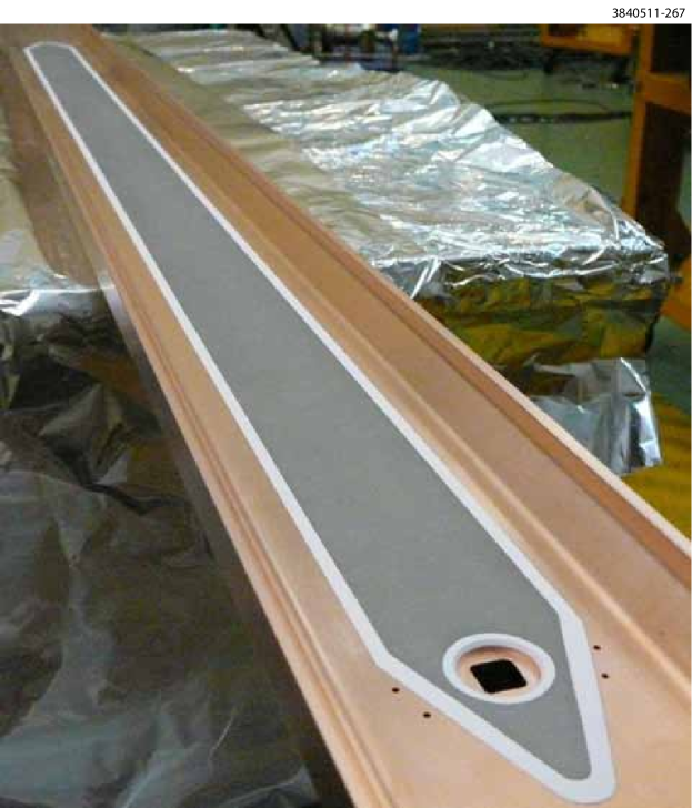
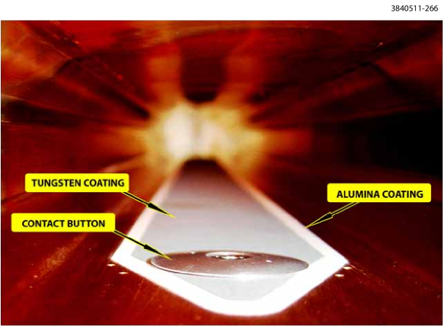
The geometry of the clearing electrode is a thin stripline [13], which consists of an alumina ceramic layer on copper surface (of approx. 0.2 mm in thickness) as an insulator and a thin layer of tungsten on the ceramic surface (of approx. 0.1 mm in thickness) as the electrode. The area of the alumina ceramic layer was larger than that of the electrode, so that the required DC voltage could be applied to the electrode in vacuum. These two layers were deposited via a thermal spray technique and were tightly bonded to the copper chamber. Tungsten was chosen as the electrode material owing to its small thermal expansion rate (as compared to the alumina ceramics), good thermal and electrical properties and substantial experience in thermal spray applications. The photograph in Figure 23 shows the finished bottom beam pipe with its deposited electrode. The insulation resistance between the electrode and the copper chamber was about 5 M (in dry air) and the electrode is capable of withholding DC voltages above 1 kV.
Since the magnetic field within the wiggler magnet is vertical, electrons will stream along field lines, impacting the top and bottom walls of the vacuum chamber and will produce secondary electrons, which subsequently stream to the opposite vacuum chamber wall. Thus the clearing electrode is designed to have a width of 40 mm and is placed on the lower wall of the vacuum chamber, extending for 1.09 m along the beamline, in order to intercept electrons impacting the bottom of the vacuum chamber. However, from the standpoint of the beam-impedance, the narrower the electrode is, the smaller the impedance. To minimize HOML induced by the electrode, the ends of the electrode are tapered at a 42∘ angle down to a 3 mm radius at its tip. The HV connection is made by a coaxial line coming through a port located underneath one of the tapered ends of the electrode. The electrical connection to the electrode is made via a convex button washer (having a 26 mm diameter) on the top of the electrode, as shown in Figure 22 and Figure 24. The connection was designed to make the inner surface (carrying the image currents from the beam) as smooth as possible, while keeping a secure electrical contact. Although the effects of the low profile of the discontinuity, the tapered ends of the electrode and the hidden HV connection have not been calculated in detail, they are expected to produce a HOML parameter of less than a few times 0.001 V/pC for the 7 to 10 mm bunch length of CESR. Any heating from the wall currents flowing on the surface of the electrode is easily handled by conduction to the beam pipe through the thin alumina dielectric layer, which has good thermal conductivity. Thermocouples mounted on the bottom beam pipe near the electrode assembly have detected no increase in heating due to HOML at any of the beam currents during operations.
At LBNL the bottom half of the beam pipe (containing the thermal-sprayed electrode) was electron beam-welded with the top half beam pipe (with all RFA features as shown in Figure 4) to form the pre-RFA beam pipe assembly and then delivered to Cornell in February 2010. Following the same assembly procedures described earlier, RFAs were inserted into the electrode beam pipe, integrated into an SCW and then installed in the L0 experimental region for CESRTA experimental runs beginning April 2010.
During stored beam operation one concern with the electrode design was the peak voltage induced by a bunch’s passing. There are two parts to this particular concern. First is that the peak voltage is high enough to either break down the dielectric layer or produce an electrical discharge in the vacuum, which could cause metal to be plated onto the dielectric. Either of these will degrade the high voltage standoff capability of the electrode. The second concern is that the voltage induced onto the electrode might couple to subsequent bunches causing enhanced HOML or transverse kicks possibly destabilizing later bunches in the train. This could be particularly a concern for the clearing electrode, since its structure resembles that of a stripline pickup or stripline kicker. Since the transmission line impedance of the electrode structure is difficult to match to the external coupling port, there can be many reflections of the induced voltage before it damps out. If the transmission line-electrical length of the electrode is chosen poorly, a resonant excitation of the beam-induced voltage could result in large voltages occurring on the electrode with respect to ground. This resonant enhancement of the voltage could lead to a sizable multiplication of all effects. Therefore the 1.05 m length of the clearing electrode was designed, after taking into account the dielectric constant of alumina of 9.8 (a reduction of the propagation delay of the signal in the stripline by a factor of 3.13 from the speed of light in vacuum), to have a round trip delay of 21.9 ns, which is not a multiple of either 4 ns or 14 ns, the primary bunch spacings employed for CESRTA.
To reduce the peak induced voltage, the ends of the electrode are tapered. As a bunch passes by the tapered end of the electrode the wall currents induced in the electrode spread out over a time equal to the difference of the propagation delay of the signal in the electrode’s stripline transmission mode and the transit time of the bunch. With a taper length of 31.3 mm, the duration of the induced signal at both ends will spread out over 0.2 ns in the forward transit direction and 0.4 ns in the reverse direction. Since the temporal standard deviation of the bunch ranges between 20 and 35 ps, spreading the induction of the signal in the electrode over more than ten times the bunch’s rise time will reduce the peak signal by a comparable factor. Since the wall currents traveling with the beam are induced into the transmission line composed of the electrode resting on the dielectric layer on top of the vacuum chamber wall, the induced voltage will be proportional to the impedance of the transmission line. With a dielectric thickness of 0.2 mm and a maximum electrode width of 44 mm, the transmission line impedance is 0.59 . At the tapered ends the impedance increases to 3.6 , thus the reflections off of the ends will cause additional (somewhat more complicated) spreading of the transmission line signal.
Some care was taken to make a reasonable match of the impedance of the external coaxial HV connection to the clearing electrode. The effective impedance of the electrode at the point where the external port attaches to the electrode’s taper is 0.78 . The hole through the beam pipe under the taper plus the HV connection post (sticking through the hole) have an impedance of 6.2 , making it impossible to match the clearing electrode’s impedance at the connection point. However, some improvement to the mismatch to the 50 type-N connector was accomplished by tapering the center conductor with a conical taper from the 50 connector to 11.5 where the center conductor attaches to the HV connection post. So in the final design there are two mismatches between electrode and the type-N connector: 1) between the electrode and the HV post and 2) between the HV post and the tapered coaxial feed line, giving reflection coefficients, respectively, of and . To allow for thermal expansion, there is a sliding contact where the conical coaxial center conductor attaches to the constant diameter, 50 center conductor.
After the construction and assembly of the electrode and the coaxial HV connection port, time domain reflectometer (TDR) measurements were made. The TDR allows a basic check of the impedance of the entire structure using a step function-signal with a rise-time of 25 ps. However, since the electrode’s transmission line impedance is so low, only an upper limit may be placed on its impedance. At the input side, the type-N connector had a reflection of + 6, while the sliding contact had additional reflections. Neither of these is very serious as they are relatively small and are contained within regions of less than 0.15 ns propagation delays. The estimated upper limit of the transmission line impedance of the central section of the clearing electrode itself is 2.6 , which is consistent with the expected 0.59 .
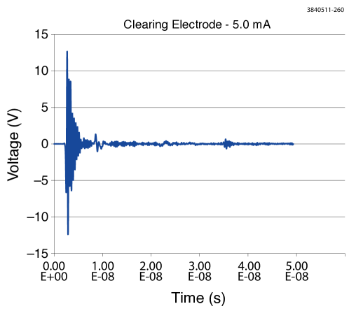
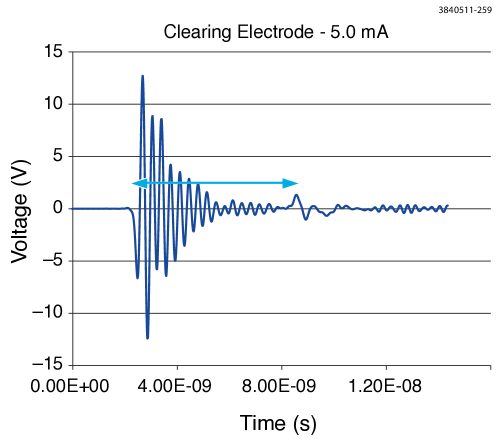
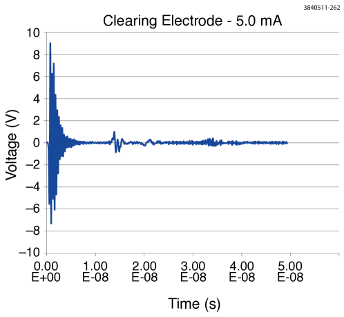
With 5 mA (8.0x10¹⁰ particles) single bunch stored electron and positron beams, measurements were made to observe the signal coming from the type-N connector at the HV input port. After installation in CESR the orientation of the clearing electrode has the HV input port oriented so that the electron bunches pass the end with the input port first and then the end with an open connection afterwards. A positron bunch circulates in the opposite direction as compared with an electron bunch. All measurements were made with 26 dB of attenuation for signal before connecting to a LeCroy Model Wavemaster 804ZI, 4 GHz bandwidth oscilloscope. In the following figures the scales have been corrected for the 26 dB of attenuation. Figures 25 and 26 show the signal from the positron single bunch on longer and shorter time scales, respectively. The signal from the positron bunch has a peak value of 13 V at the time of the bunch’s passage by the HV coupling port as is indicated by the 2.9 GHz burst. Although a detailed model for the coupling from this tapered stripline has not been constructed, this frequency appears to be characteristic of the propagation delay along the taper. Figure 26 shows in more detail the signal induced at the HV coupling port (as described above) and the open taper at the far end. Although the signal from the positron bunch was induced at the open taper earlier, due to the propagation delay from the dielectric insulator, this signal arrives at the HV coupling port 0.61 ns later than the signal induced in the tapered end connected to the HV coupling port. The time segment marked in figure 26 is approximately the delay from the beam transit velocity and the signal propagation velocity. Likewise, the signal observed from the 5 mA electron bunch, seen in figures 27 and 28 (viewed on longer and shorter timescales, respectively), shows the same high frequency burst from the taper at the HV coupling port followed by the lower bandwidth pulse from the open tapered end of the electrode. In this case the peak signal observed in the HV input port is 9 V and the delay between the signals at the two ends has increased to 1.33 ns. The longer delay is caused by the fact that the bunch must transit the length of the electrode at and then the signal induced in the open taper must propagate back at . By comparing the delays between these two signals for positrons and electrons, it is possible to determine the measured propagation delay in the transmission line defined by the clearing electrode and, hence, the dielectric constant for the alumina. These measurements yield a dielectric constant of 2.9 in good agreement with the expected 3.13 value.
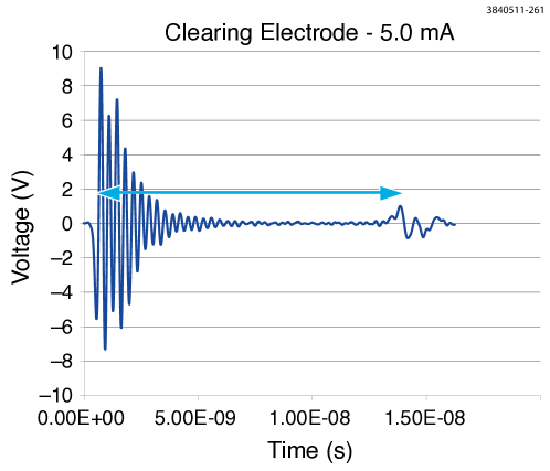
Neither of the positron or electron beam induced signals, as viewed at the HV coupling port, suggest serious peak voltages for the electrode at any typical operating currents for CESRTA. They also suggest that the reflections decay in only a small number of traversals along the electrode and that taken with the measured propagation delays imply that resonant build-up of the signals from multiple bunches within trains will not be a problem.
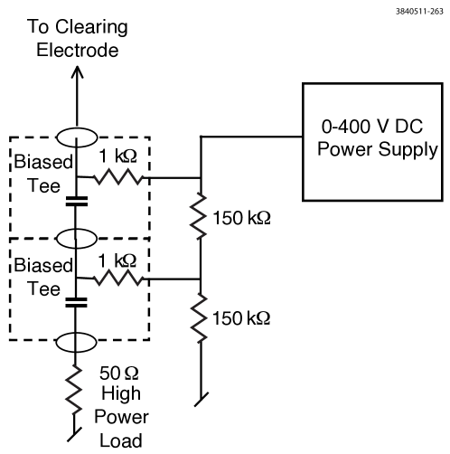
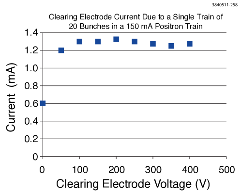
The last of the post-installation measurements was made after attaching the HV coupling network and measuring the electrode current vs. electrode voltage for a given beam current. The coupling network and its HV DC power supply are shown in figure 29; the network is constructed from bias tees, which were purchased from MECA (part number 200N-MF-1), capable of a peak 200 V DC bias and rated to withstand a 300 W average RF power and 3 kW peak RF power. Two of these were cascaded to obtain the needed 400 V bias capability for the CESRTA studies. During bench testing of the MECA units, it was apparent that they had an unpleasant notched response just below about 100 MHz. Anticipating that this could be a problem, the bias tees that were modified by replacing the originally installed inductor with a 1 k resistor. The frequency response is improved and now has a single pole high pass cutoff frequency of about 30 MHz. Figure 30 gives the measured clearing electrode current as a function of bias voltage for a train of 20 positron bunches at 5.3 GeV, while the superconducting wiggler is unpowered. Note that 100 V of bias is enough to saturate the clearing electrode’s collection current.
After operations for three CESRTA runs and two CHESS X-ray User runs (from April to December 2010) with peak bunch currents of over 9 mA, a visual inspection of the electrode and the electric contact was performed during the January 2011 shutdown. The clearing electrode’s appearance was the same as it was during its installation. With an accumulated total beam dose exceeding 1000 Amphr over the CESRTA and CHESS runs, the electrode and the electrical contact were found to be in excellent condition with no sign of any arcing or plating of material anywhere inside of the vacuum chamber.
2.7 Experimental Results
Over many CESRTA experimental runs data was acquired using the RFAs installed in the SCWs. This included studies in each of the experimental chambers as described above. Results of some of these measurements may be found in the following publication[14].
3 Summary
The installation of a significant number of vacuum chambers with their associated diagnostics were required for the modification of the storage ring CESR to support the creation of CESRTA, a test accelerator configured to study accelerator beam physics issues for a wide range of accelerator effects and to develop instrumentation related to present light sources and future lepton damping rings. This paper has presented many of the details for the modifications of the superconducting wigglers to accommodate the diagnostic instrumentation for the study of EC behavior within wigglers. This paper is a useful reference for any future analysis of the CESRTA measurements of electron clouds in superconducting wigglers. As part of the larger CESRTA program, CESR’s vacuum system and instrumentation have been optimized for the study of low emittance tuning methods, electron cloud effects, intra-beam scattering, fast ion instabilities as well as the development and improvement of beam diagnostics.
Acknowledgements
The authors would like to acknowledge the many contributions that have helped make the CESRTA research program a success. It would not have occurred without the support of the International Linear Collider Global Design Effort led by Barry Barish. Furthermore, our colleagues in the electron cloud research community have provided countless hours of useful discussion and have been uniformly supportive of our research goals.
We would also like to thank the technical and research staff at Cornell’s Laboratory for Accelerator ScienceS and Education (CLASSE) for their efforts in maintaining and upgrading CESR for Test Accelerator operations. Specifically we would like to acknowledge the contributions of a few individuals during this portion of the project: Margie Carrier performed the majority of RFA (in-vacuum) electric assembly, which was extremely complex and tedious. James Sears and Brian Clasby made significant contributions to the e-beam welding of the final RFA cover. They had to add an extension to the Newman Laboratory electron-beam welder chamber, re-program the e-beam welding head, work out detailed welding parameters, etc. Ken Powers assisted with the removal of old SCW beampipes and preparations of the SCEs for the RFA beampipes. Mike Palmer produced excellent welding results for the final assembling of the RFA beampipes into the SCWs.
Finally, the authors would like to acknowledge the funding agencies that helped support the program. The U.S. National Science Foundation and Department of Energy implemented a joint agreement to fund the CESRTA effort under contracts PHY-0724867 and DE-FC02-08ER41538, respectively. Further program support was provided by the Japan/US Cooperation Program. Finally, the beam dynamics simulations utilized the resources off the National Energy Research Scientific Computing Center (NERSC) which is supported by the Office of Science in the U.S. Department of Energy under contract DE-AC02-05CH11231.
References
- [1] M. Billing, The conversion of CESR to operate as the Test Accelerator, CesrTA. Part 1: overview, J. Instrum. 10 (2015).
- [2] M. G. Billing and Y. Li, The conversion of CESR to operate as the test accelerator, CesrTA, part 2: Vacuum modifications, J. Instrum. 10 (2015).
- [3] M. G. Billing, J. V. Conway, J. A. Crittenden, S. Greenwald, Y. Li, R. E. Meller, C. R. Strohman, J. P. Sikora, J. R. Calvey, and M. A. Palmer, The conversion of CESR to operate as the test accelerator, CesrTA, part 3: Electron cloud diagnostics, J. Instrum. 11 (2016).
- [4] Y. He, G. Codner, R. D. Ehrlich, Y. Li, V. Medjidzade, A. Mikhailichenko, N. B. Mistry, E. Nordberg, D. Rice, D. Sabol, K. Smolenski, D. Widger, and E. N. Smith, Design and operation of the cryostat for the CESR-c superconducting wiggler magnets, Proceedings of the 2003 Particle Accelerator Conference, Portland, OR (Joe Chew, Peter Lucas, and Sara Webber, eds.), IEEE, 2003, pp. 2399–2401.
- [5] J. A. Crittenden, M. A. Palmer, and D. L. Rubin, Wiggler magnet design development for the ILC damping rings, Proceedings of the 2012 International Particle Accelerator Conference, New Orleans, LA, IEEE, 2012, pp. 1969–1971.
- [6] L. Wang and F. Zimmermann, Electron cloud in the wigglers of the positron damping ring of the International Linear Collider, Proceedings of the 2007 Particle Accelerator Conference, Albuquerque, NM (C. Petit-Jean-Genaz, ed.), IEEE, 2007, pp. 1808–1810.
- [7] J. R. Calvey, W. Hartung, Y. Li, J. A. Livezey, J. Makita, M. A. Palmer, and D. Rubin, Comparison of electron cloud mitigating coatings using retarding field analyzers, Nucl. Instrum. Methods Phys. Res. A760 (2014), 86–97.
- [8] G. Stupakov and M. Pivi, Suppression of the effective secondary emission yield for a grooved metal surface, Proceedings of ECLOUD 2004: 31st ICFA Advanced Beam Dynamics Workshop on Electron-Cloud Effects, Napa, CA (Geneva, Switzerland) (M. Furman, S. Henderson, and F. Zimmerman, eds.), no. CERN-2005-001, CERN, 2004, pp. 139–141.
- [9] M. Pivi, F. K. King, R. E. Kirby, T. O. Raubenheimer, G. Stupakov, and F. Le Pimpec, Sharp reduction of the secondary electron emission yield from grooved surfaces, J. Appl. Phys. 104 (2008).
- [10] A. A. Krasnov, Molecular pumping properties of the LHC arc beam pipe and effective secondary electron emission from Cu surface with artificial roughness, Vacuum 73 (2004), 195–199.
- [11] L. Wang, T. O. Raubenheimer, and G. Stupakov, Suppression of secondary emission in a magnetic field using triangular and rectangular surfaces, Nucl. Instrum. Methods Phys. Res. A571 (2007), 588–598.
- [12] L. Wang, private communication.
- [13] Y. Suetsugu, H. Fukuma, L. Wang, M. Pivi, A. Morishige, Y. Suzuki, M. Tsukamoto, and M. Tsuchiya, Demonstration of electron clearing effect by means of a clearing electrode in high-intensity positron ring, Nucl. Instrum. Methods Phys. Res. A598 (2009), 372–378.
- [14] J. R. Calvey, W. Hartung, Y. Li, J. A. Livezey, J. Makita, M. A. Palmer, and D. Rubin, Measurements of electron cloud growth and mitigation in dipole, quadrupole, and wiggler magnets, Nucl. Instrum. Methods Phys. Res. A770 (2015), 141–154.