High degree of current rectification at nanoscale level
Abstract
We address an unexpectedly large rectification using a simple quantum wire with correlated site potentials. The external electric field, associated with voltage bias, leads to unequal charge currents for two different polarities of external bias and this effect is further enhanced by incorporating the asymmetry in wire-to-electrode coupling. Our calculations suggest that in some cases almost cent percent rectification is obtained for a wide bias window. This performance is valid against disorder configurations and thus we can expect an experimental verification of our theoretical analysis in near future.
I Introduction
Designing of an efficient rectifier at nanoscale level has been the subject of intense research after the prediction of molecular rectifier by Aviram and Ratner r1 in . Following this pioneering work, interest in this area has rapidly picked up with several theoretical propositions and experimental verifications and most of these works involve small organic molecules with donor-acceptor pair between metallic electrodes r2 ; r3 ; r4 ; r5 ; r55 ; r6 ; r7 ; r8 ; r9 ; r10 ; r11 ; r12 . Recently a DNA-based rectifier has also been established r13 which exhibits a large rectification ratio of about at V.
To achieve rectification (viz, ), energy levels of the bridging material have to be aligned differently for the positive and
negative biases. This can be done in two different ways: (i) placing an asymmetric conductor between source and drain electrodes r9 ; r11 , keeping identical conductor-to-electrode couplings, and (ii) considering a symmetric conductor with unequal conductor-electrode couplings r12 . The understanding is that for both these two cases resonant energy levels, in presence of finite bias, are arranged distinctly for two different biased conditions which results finite rectification. Therefore, when both these two conditions are satisfied one can expect maximum rectification.
So far mostly molecular systems r6 ; r7 ; r8 ; r9 ; r10 ; r11 ; r12 have been used to design rectifying diodes, but constructing them using single molecules is a major challenge janes and still many open questions remain which certainly demand further study. Therefore, designing of a rectifier using simple geometric structure which provides high rectification ratio is a matter of great interest. In the present work we essentially focus on it and make an attempt to establish that a simple D chain with correlated site potentials can exhibit a very high degree of rectification, and sometimes it becomes nearly close to for a wide bias window. This performance is valid against disordered configurations which we confirm by comparing the results of different D quasi-periodic chains like Fibonacci (Fibo), Thou-Morse (TM), Copper-mean (CM) and Bronze-mean (BM) and all these systems are constructed by using two primary lattices, namely and , following the specific inflation rules quasiall ; tm ; skmfib . For the case of Fibonacci chain the rule is: and . Therefore, applying successively this substitutional rule, staring with or lattice we can construct the full lattice chain for any particular generation, say -th generation, obeying the prescription . So, if we start with lattice then the first few generations of the Fibonacci series are , , , , , , etc. The inflation rules for the other three quasiperiodic chains which we consider here i.e., TM, CM and BM are: , ; , , and , , respectively. Using these rules we construct the quasiperiodic chains for any desired generation starting with any lattice site or .
The rest of the paper is arranged as follows. In Sec. II we present the model and theoretical framework for calculations. The results are described in Sec. III, and finally, in Sec. IV we conclude our findings.
II Model and theoretical framework
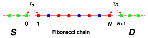
The calculations are worked out using wave-guide theory based on tight-binding (TB) framework. In this framework the Hamiltonian of the full system, schematically shown in Fig. 1, can be written as , where , and correspond to the Hamiltonians of the electrodes (source and drain), quasi-periodic chain and chain-to-electrode tunneling coupling, respectively. In terms of on-site potential and nearest-neighbor hopping integral , the TB Hamiltonian of the chain can be written as:
| (1) |
where () represents the electronic creation
(annihilation) operator. In a similar way we can write the TB Hamiltonian of the two side-attached perfect D electrodes parameterized by and . These electrodes are coupled to the sites and of the conductor (described by ) through the coupling parameters and (see Fig. 1), where being the total number of lattice sites of the bridging conductor.
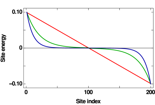
In presence of a finite bias between the source and drain, an electric field is developed across the chain and hence its site energies are voltage dependent el1 ; el2 . It gives , where is voltage independent and it becomes or depending on the lattice sites or . The dependence of is associated with electron screening as well as bare electric field at the junction. In the absence of any screening electric field is uniform across the junction el1 ; el2 which makes (linear variation, red line of Fig. 2) for a -site chain. Whereas, long-range electron screening makes the profile non-linear as shown by the green and blue curves of Fig. 2. In our calculations we consider these three different potential profiles to have a complete idea about the bare and the screened electric field profiles, and their effects on rectification as in realistic case different materials possess different electron screening which will yield different field variations. For a slight variation from these potential profiles no significant change is observed in the physical properties, and thus our findings may be implemented in realistic cases.
To evaluate transmission probability across the conducting junction we solve a set of coupled linear equations containing wave amplitudes of distinct lattice sites of the chain wg ; skm . Assuming a plane wave incidence, we can write the wave amplitude at any site of the source as , where is the wave-vector and being the reflection coefficient. While, for the drain electrode we get , where represents the transmission coefficient. For each , associated with the injecting electron energy, we find the transmission probability from the expression . Once it is determined, the net junction current for a particular bias voltage at absolute zero temperature is obtained from the relation datta
| (2) |
where represents the Fermi energy. Finally, we define the rectification ratio as r13 . suggests no rectification. In all calculations we set the common parameter values as: eV, , eV and, unless otherwise stated .
III Results and discussion
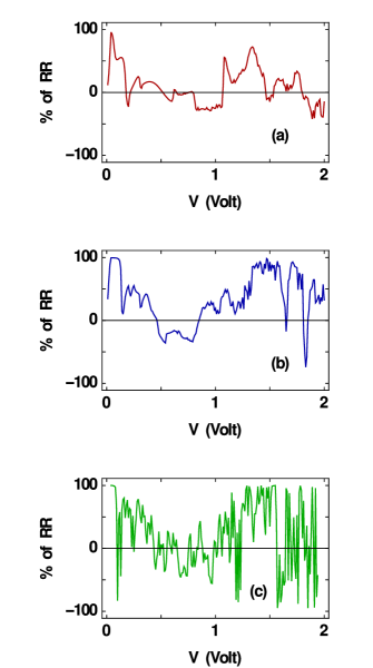
Now we present our results. In Fig. 3 we show the variations of
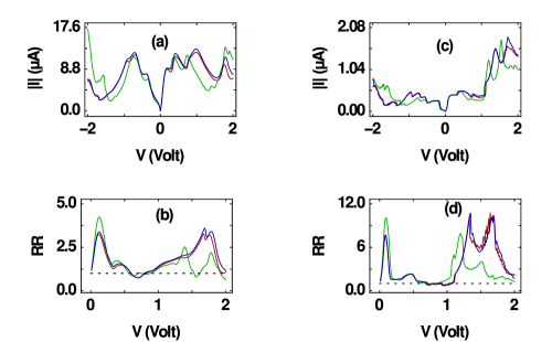
both for the forward and reverse biased conditions along with the rectification ratio considering three different electrostatic potential profiles where the first and second columns correspond to the symmetric and asymmetric wire-to-electrode couplings, respectively. Two observations are noteworthy. First, the currents for the positive and negative biases are quite close to each other in the limit of symmetric coupling (Fig. 3(a)), whereas they differ distinctively in the case of asymmetric coupling (Fig. 3(c)) though the currents in this case are much less than the previous one. Second, for a wide bias window (-V) the rectification ratio is significantly large, in the limit of asymmetric coupling, reaching a maximum of . This is a reasonably large value compared to the reported results for different conducting junctions considering both symmetric molecular structures as well as asymmetric molecule-to-lead couplings where RR varies between to r9 ; r12 .
To illustrate the mechanism of rectification let us focus on the spectra given in Fig. 4. For the fully perfect chain (), - spectrum in presence of positive bias (red curve of Fig. 4(a)) exactly matches with what we get in the case of negative
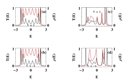
bias (red curve of Fig. 4(b)). Therefore, for this junction identical currents are obtained upon the integration of the transmission function , resulting a vanishing rectification. While, comparing the spectra given in Figs. 4(c) and (d), worked out for the positive and negative biases considering a Fibonacci chain, it is clearly seen that the transmission spectra differ sharply which results a finite rectification. To achieve rectification the essential thing is that, as stated earlier, the energy levels of the bridging material have to be aligned differently for the positive and negative biases. The alignments of energy levels for the two different wires are clearly reflected from the - spectra (black curves of Fig. 4). Thus increasing the misalignment higher is expected and it can be done further by including additional asymmetric factors like asymmetric environmental effects env , inconsistent gating gat , etc.
Figure 5 shows the percentage of rectification (defined as ) as a function of voltage for three different sizes of the Fibonacci chain. Quite interestingly we see that for wide voltage regions nearly cent percent rectification is obtained, and thus the present system can be utilized as a perfect rectifier.
In order to justify the robustness of rectification against disorderness, in Fig. 6 we present - characteristics for some typical quasi-periodic lattices. All these junctions provide finite rectification where varies in a wide range, and from these curves it can be emphasized that any one of such lattices can be used to achieve
the goal of rectification action. Looking carefully into the spectrum (Fig. 6) it is observed that reaches to zero ()
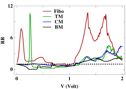
for a reasonable voltage window (-V) for the junction containing BM wire. One could also get opposite scenario i.e., rectification through any one of these junctions. This is solely associated with the interplay between the arrangements of lattice sites and electrostatic potential profile.
Finally, in Fig. 7 we discuss the possibilities of regulating the rectification ratio externally for a fixed bias voltage. This can be
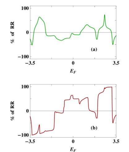
achieved by tuning the Fermi energy, which on the other hand is controlled by external gate voltage. It is worthy to note that upon changing one can get a wide variation of (viz, to ), and thus it can be emphasized that the present model can be utilized to get externally controlled rectifier at nano-scale level.
Before the end, we would like to point out that, apart from rectifying action all these quantum wires characterized by quasi-periodic lattices show another uncommon property of junction current where an increase in the bias voltage results a reduction of net current (see Figs. 3 and 6). This is the so-called negative differential conductance (NDC) effect ndc , and its detailed analysis will be given in our forthcoming paper.
IV Concluding remarks
To conclude, in the present work we have attempted to establish a model quantum system that can exhibit a high degree of current rectification at nanoscale level. An unexpectedly large rectification ratio has been obtained, and most importantly, we see that in some cases nearly cent percent rectification can be achieved for a wide bias window. Our results are also valid against disordered configurations which we have confirmed by considering different kinds of disordered systems. Though the proposition given here is based on purely theoretical arguments, we hope that its experimental verification can be done in near future.
Finally, we want to note that although the results have been worked out at zero temperature, all the physical features remain invariant at finite temperature ( K) as thermal broadening of energy levels is much weaker than the broadening caused as a result of wire-to-electrode couplings datta .
V Acknowledgment
MS would like to acknowledge University Grants Commission (UGC) of India for her research fellowship.
References
- (1) A. Aviram and M. A. Ratner, Chem. Phys. Lett. 29, 277 (1974).
- (2) A. Dhirani, P. -H. Lin, P. Guyot-Sionnest, R. W. Zehner, and L. R. Sita, J. Chem. Phys. 106, 5249 (1997).
- (3) C. Zhou, M. R. Deshpande, M. A. Reed, L. Jones II, and J. M. Tour, Appl. Phys. Lett. 71, 611 (1997).
- (4) J. Frantti, V. Lantto, S. Nishio, and M. Kakihana, Phys. Rev. B 59, 12 (1999).
- (5) R. M. Metzger, Acc. Chem. Res. 32, 950 (1999).
- (6) J. Taylor, M. Brandbyge, and K. Stokbro, Phys. Rev. Lett. 89, 138301 (2002).
- (7) G. J. Ashwell, W. D. Tyrrell, and A. J. Whittam, J. Am. Chem. Soc. 126, 7102 (2004).
- (8) I. Díez-Pérez et al., Nature Chem. 1, 635 (2009).
- (9) C. A. Nijhuis, W. F. Reus, and G. M. Whitesides, J. Am. Chem. Soc. 132, 18386 (2010).
- (10) S. K. Yee et al., ACS Nano 5, 9256 (2011).
- (11) A. Batra et al., Nano Lett. 13, 6233 (2013).
- (12) H. J. Yoon et al., J. Am. Chem. Soc. 136, 17155 (2014).
- (13) K. Wang, J. Zhou, J. M. Hamill, and B. Xu, J. Chem. Phys. 141, 054712 (2014).
- (14) C. Guo et al., Nature Chem. 8, 484 (2016).
- (15) D. Janes, Nature Chem. 1, 601 (2009).
- (16) A. M. Guo, Phys. Rev. E 75, 061915 (2007).
- (17) H. Lei, J. Chen, G. Nouet, S. Feng, Q. Gong, and X. Jiang, Phys. Rev. B 75, 205109 (2007).
- (18) M. Patra and S. K. Maiti, Ann. Phys. 375, 337 (2016).
- (19) S. Pleutin, H. Grabert, G. L. Ingold, and A. Nitzan, J. Chem. Phys. 118, 3756 (2003).
- (20) S. K. Maiti and A. Nitzan, Phys. Lett. A 377, 1205 (2013).
- (21) Y. J. Xiong and X. T. Liang, Phys. Lett. A 330, 307 (2004).
- (22) M. Patra and S. K. Maiti, Sci. Rep. 7, 43343 (2017).
- (23) Datta, S. Electronic transport in mesoscopic systems. Cambridge University Press, Cambridge (1997).
- (24) B. Capozzi et al., Nature Nanotech. 10, 522 (2015).
- (25) B. Capozzi et al., Nano Lett. 14, 1400 (2014).
- (26) B. Xu and Y. Dubi, J. Phys.: Condens. Matter 27, 263202 (2015).