Microwave-Induced Oscillations in the Magnetocapacitance: Direct Evidence for Non-equilibrium Occupation of Electronic States
Abstract
In a two-dimensional electron system, microwave radiation may induce giant resistance oscillations. Their origin has been debated controversially and numerous mechanisms based on very different physical phenomena have been invoked. However none of them have been unambiguously experimentally identified, since they produce similar effects in transport studies. The capacitance of a two-subband system is sensitive to a redistribution of electrons over energy states, since it entails a shift of the electron charge perpendicular to the plane. In such a system microwave induced magnetocapacitance oscillations have been observed. They can only be accounted for by an electron distribution function oscillating with energy due to Landau quantization, one of the quantum mechanisms proposed for the resistance oscillations.
pacs:
73.21.Fg, 73.30.+y, 73.50.GrRecent studies of non-equilibrium phenomena in two-dimensional electron systems (2DES) exposed to microwave (MW) radiation have revealed remarkable transport effects. The most prominent one is the appearance of giant microwave-induced magnetoresistance oscillations (MIRO) Zudov1 ; Ye . In the main minima the resistance may approach zero and so-called zero resistance states develop Mani ; Zudov2 ; Dorozh2015 . MIRO have proved to be a general effect as they by now have been observed in both degenerate 2DES, such as in GaAs/AlGaAs Zudov1 ; Ye , Si/SiGe ZudovSi and ZnO/MgZnO ZnO heterostructures, as well as in non-degenerate 2D electron gases on liquid helium KonstHe (for additional references we refer to the review DmitrievRMP ). MIRO are periodic in , where is the MW frequency and is the cyclotron frequency. The proposed explanations of MIRO are based on classical or quantum effects as reviewed in Ref. DmitrievRMP (see also a recent classical theory DyakonovPRL16 ). Despite significant progress and a satisfactory description of much of the phenomenology by some of the proposed mechanisms, the theoretical dispute has not been settled since crucial unresolved issues remain. In particular, the absence of a dependence of MIRO on the MW circular polarization direction Smet ; Ganichev continues to stimulate new theoretical ideas involving edge Shep and contact Mikhailov phenomena and invigorates the debate ZudovComm ; MikhailovComm . Magnetotransport experiments alone are likely insufficient to identify unambiguously all mechanisms active in experiment. Apart from MIRO, oscillations of the same periodicity were also found elsewhere in other electronic transport properties. Under MW radiation voltages and currents develop even in the absence of external sources. These photo-galvanic signals Willett ; Bykov ; Dorozh09 can be traced back to MIRO and the MW induced changes in the dc-conductivity PRB09 ; PRB11 . Therefore they too are of limited use to reduce the clutter. There is clearly a strong need to look at other physical quantities than the conductivity.
Here, using the magnetocapacitance technique and a suitable sample design we demonstrate that MW radiation generates a non-equilibrium distribution of electrons among the Landau levels oscillating with energy. Such a non-equilibrium distribution function Dorozh03 ; Dmitriev03 ; Dmitriev05 ; Raichev represents one of the most elaborate theoretical pictures to account for MIRO as a bulk quantum phenomenon. While capacitive measurements in the presence of the MW radiation have been reported for quasi-2D electrons above a He surface Abdur ; Chep , in degenerate 2DES the capacitance has not been addressed yet in this microwave context. It has also been widely used for studying the equilibrium 2DES compressibility Stiles . The sample consists of a field effect transistor with a back gate and an electron channel that resides in an asymmetric, wide GaAs quantum well (QW) with two occupied subbands. A microwave induced redistribution of the electrons along the energy scale modifies the occupation of both subbands and is accompanied by a shift of the electrons perpendicular to the QW plane. This shift alters the capacitance which is primarily sensitive to the occupation of the highest subband whose wave function is located closer to the gate. Hence, the capacitance can capture directly microwave induced oscillations in the electron energy distribution. The sensitivity to vertical electron shifts is what distinguishes this capacitance measurement from all previous transport experiments. A second frequently invoked mechanism Ryzhii1 ; Ryzhii2 ; Durst ; Ryzhii3 ; Aleiner ; Dmitriev09 to explain MIRO involves a microwave induced impurity scattering assisted displacement of the electrons in the plane. The equations describing MIRO within this displacement model are, except for a temperature dependent prefactor, identical to the equations obtained from a picture based on a non-equilibrium energy distribution function Dmitriev05 ; Dmitriev09 . An unambiguous separation of these two possible contributions is therefore non-trivial. The capacitance measurements can not exclude that the displacement mechanism is active in MIRO as they are not sensitive to lateral displacements. However, they can without any ambiguity prove the formation of a non-trivial electron energy distribution function by the microwaves and thereby provide support for a bulk quantum origin of MIRO.
We measured two identical Hall bar samples processed side by side on the same piece of a GaAs/AlGaAs heterostructure. The electron system resides in a 60 nm wide GaAs QW. An in-situ grown back gate allows to tune density and measure the capacitance. In these samples the second subband gets populated at total electron density for a gate voltage , as will be shown below. Further experimental details are deferred to the Supplemental Material Supp . The samples were placed in a stainless steel tube with a diameter of 18 mm. It served as an oversized waveguide for the MW radiation whose frequency was varied from 54 to 78 GHz. The measurements were performed in a pumped liquid at 0.5 K.
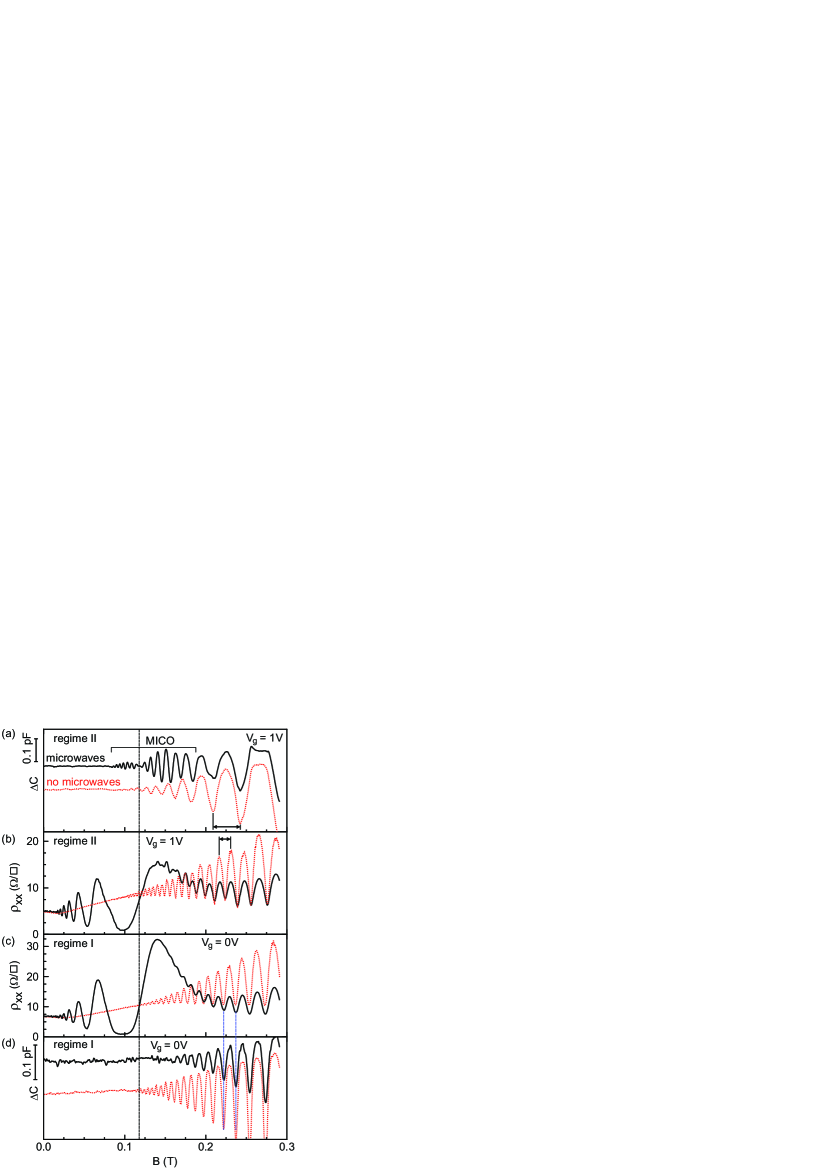
Fig. 1 illustrates the behavior of the longitudinal resistivity, (panels b and c), and variation of the capacitance (panels a and d),in the absence and presence of MW radiation for two gate voltages: and 1 V. As shown below, these voltages correspond to one and two occupied subbands, respectively. While the curves (panels b and c) look very similar in both regimes, the magnetocapacitance traces in panels a and d are qualitatively different. A close inspection allows to identify four types of -periodic oscillations. At high -fields all traces exhibit the well-known Shubnikov-de Haas (SdH) oscillations. The microwaves induce additional, large oscillations in the magnetoresistivity. These are just MIRO. The oscillations in the magnetocapacitance measured in the absence of radiation reflect the oscillations in the thermodynamic density of states (DOS), Stiles , brought about by Landau quantization. Here is the chemical potential of the 2DES. The MW radiation suppresses the amplitude of these DOS oscillations in the magnetocapacitance. In the density regime with only one occupied subband (regime I) shown in panel d, the suppression is the only effect of the radiation on the capacitance. In contrast, when two subbands are occupied (regime II) the MW radiation induces additional oscillations with a new period. These microwave induced capacitance oscillations, hereafter referred to as MICO, have been demarcated in panel a. They exhibit a node at the same -field where the MIRO have their rightmost zero, i.e., when . This is highlighted by the dashed line in Fig.1. It corresponds to the cyclotron resonance (CR) of electrons with effective mass . This value of is close to the recently obtained Zudovm from the MIRO periodicity. The observation of MICO is the key experimental result of this Letter.
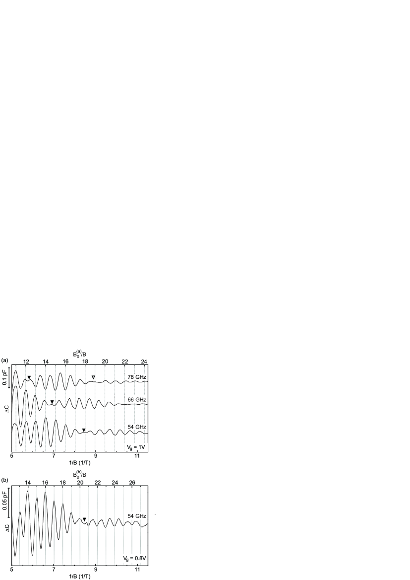
In Fig.2a MICO have been plotted as a function of for three different MW frequencies to highlight the following: (i) The oscillations are indeed periodic in and the period does not depend on the frequency. (ii) The oscillation amplitude indeed reveals a beating pattern with the leftmost node located at the CR (for ). (iii) When crossing a node the phase of the oscillations jumps by . This can be seen most easily with the help of the top axis. The abscissa is obtained by normalizing with the oscillation period: . Integer values initially correspond to maxima. However, when the CR node is crossed, integer values align with minima instead. In the topmost curve for 78 GHz radiation, a second node at is observed. When it is crossed, integer values correspond again to maxima. The data in panel b have been recorded at the same frequency as the bottom trace in panel a, but for a different . A comparison unveils that the MICO periodicity has changed while the node stays at the CR position.
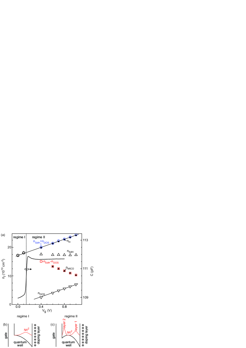
To identify the origin of MICO, it is instrumental to systematically vary , monitor changes in the oscillation period and compare the results for different oscillation types. The outcome of such a study is summarized in Fig. 3a. The SdH and DOS oscillations, also observed under equilibrium conditions, help to extract the density and identify when a second subband gets populated. At where only one subband is occupied, the SdH and DOS oscillations have the same period and phase as seen in panels c and d of Fig. 1 (short vertical lines). Minima appear when the Fermi level is located within a cyclotron gap and an integer number of spin degenerate Landau levels is occupied. This occurs at -fields for which with , the Landau level degeneracy per spin and the density in the lowest subband. It results in a 1/B-periodicity equal to from which can be calculated. However, more generally, this expression can be used to convert any observed periodicity into a density whose meaning needs to be interpreted properly. Hereafter, the densities extracted from SdH and DOS oscillations as well as MICO will be denoted as with subscript SdH, DOS or MICO. They have been plotted in Fig. 3a together with deduced from the Hall resistance at low . The latter increases with at a constant rate. When tracing and to positive in Fig. 3a, we note that their behavior is very different. For instance, remains approximately constant. Referring to the raw data recorded at (Fig. 1b), the envelope of the SdH oscillation pattern has become more complicated but its main period indeed remains close to that at . On the other hand, drops considerably when exceeds 0.15 V. This is also apparent in the raw data of Fig. 1 where the horizontal arrows in panels a and b mark the oscillation periods. In Fig. 3a also the sum has been plotted. It coincides with for . In regime I, all densities are equal: . We assert that all these observations can be understood straightforwardly assuming the second subband becomes occupied for .
In a wide QW with an asymmetric potential profile, subband wave functions are located at different distances from the gate effectively mimicking a bilayer system as schematically illustrated in panel c of Fig. 3. For such a case, a variation of primarily changes the density in the second subband or layer 2 closest to the gate and only slightly affects the charge in remote layer 1 (the first subband). Then, the DOS oscillations are determined by Landau quantization in the second subband and their periodicity is governed by the density in this subband, , only (for more details see Refs. Dolgopolov ; Dorozh2016 ). Back to the SdH oscillations, one may expect two sets of oscillations, determined by carrier densities in both subbands, and . In our raw data the fastest oscillations are however easiest to discern. They are associated with Landau quantization of the lowest subband with the largest population, , which remains approximately fixed since the gate electric field is screened by the electrons in the second subband. These electrons generate weaker oscillations in the envelope of the rapid oscillations from the first subband. We note that the linear dependence as well as nearly constant value of shown in Fig.3(a) are similar to those reported in other studies of unbalanced bilayer electron systems (see, for example, Refs. Stoermer ; Shayegan for single and double quantum wells, respectively). The Hall density corresponds to the total density . This interpretation of the data is strongly supported by the experimentally established relation . Then we finally conclude that and . Fig. 3a also contains the density extracted from MICO, . Apparently it is identical to , which in view of the above discussion is equivalent to the subband population difference: .
Clearly, the response to radiation is very different in and the magnetocapacitance. It follows that MICO cannot be explained in terms of a MW induced variation of the conductivity. The extracted density from MICO points to its origin, since the condition is equivalent to where () are the subband energies. At this commensurability condition, Landau levels of the two subbands are aligned. We therefore argue that MICO reflect a MW induced charge redistribution among the two subbands whose magnitude oscillates with . This is detected in the capacitance since, in our sample, it selectively responds to occupation of the second subband. This interpretation is further corroborated by the capacitance step observed in Fig. 3a at V. This step is caused by occupation of the second subband (i.e., formation of the second layer) with a center of mass of the wave function located approximately 20 nm closer to the gate than that of the 2DES in regime I at V (compare Figs 3b and 3c). It demonstrates sensitivity of our measurements to variation of the charge distribution in the QW. For the sake of completeness, we note that also magnetointersubband oscillations (MISO) with a period determined by the relation may occur in the magnetoresistance due to intersubband scattering Polyan ; SST1 ; SST2 ; PRB46 ; Raikh . They can be strongly affected by radiation, which may introduce nodes Bykov2 ; Raichev . They can be explained by both non-equilibrium distribution function and displacement mechanisms Raichev ; Raichev2 . At 0.5 K the MISO are masked by the SdH oscillations.
To substantiate our assertion that the magnetocapacitance oscillations prove that microwaves create a non-equilibrium distribution function oscillating with energy due to Landau quantization, we have analyzed our results within a distribution function model generalized to the case of two occupied subbands Raichev . The equation for the MW induced correction to the Fermi distribution function in a balanced double-quantum well structure reads as follows Raichev :
| (1) |
The dimensionless factor is proportional to the MW power absorbed by the 2DES. This equation is derived to first order with respect to the small Dingle factors for each subband and under the assumptions that . Here, is the electron quantum lifetime in the -th subband and is the Fermi energy. Within this framework of approximations, the density of states in a subband is given by
| (2) |
The MW induced variation of the density in the first subband () is equal to
| (3) |
When , Eq.(3) describes magnetooscillations with a periodicity determined by the commensurability between the cyclotron energy and the subband spacing: . The beating pattern and nodes are caused by the factor . The nodes are located at . This oscillation pattern described by Eq.(3) matches all the observed features of MICO. These oscillations should also persist in unbalanced system in which the center of mass of the wave functions of the two subbands are spatially separated. Then the oscillating redistribution of electrons between the subbands (i.e., the layers) , produces oscillations in the capacitance. This accounts for our experimental observations.
In summary, by implementing a new experimental approach to study non-equilibrium phenomena in 2DES we have discovered microwave induced magnetooscillations of an electrical capacitance. We have shown that these oscillations reflect redistribution of electrons between two occupied subbands which oscillates with magnetic field due to non-trivial distribution of electrons among Landau levels. Our observation establishes unequivocally the importance of this non-equilibrium distribution function scenario which was developed to explain MIRO.
We acknowledge fruitful discussions with I. A. Dmitriev. Experiment and data evaluation of this work were supported by the Russian Scientific Foundation (Grant 14-12-00599). JHS and VU acknowledge support from the GIF.
References
- (1) M. A. Zudov, R. R. Du, J. A. Simmons, and J. L. Reno, Phys. Rev. B 64, 201311(R) (2001).
- (2) P. D. Ye, L. W. Engel, D. C. Tsui, J. A. Simmons, J. R. Wendt, G. A. Vawter, and J. L. Reno, Appl. Phys. Lett. 79, 2193 (2001).
- (3) R. G. Mani, J. H. Smet, K. von Klitzing, V. Narayanamurti, W. B. Jonson, and V. Umansky, Nature 420, 646 (2002).
- (4) M. A. Zudov, R. R. Du, L. N. Pfeiffer, and K. W. West, Phys. Rev. Lett. 90, 046807 (2003).
- (5) S. I. Dorozhkin, V. Umansky, L. N. Pfeiffer, K. W. West, K. Baldwin, K. von Klitzing, and J. H. Smet, Phys. Rev. Lett. 114, 176808 (2015).
- (6) M. A. Zudov, O. A. Mironov, Q. A. Ebner, P. D. Martin, Q. Shi, and D. R. Leadley, Phys. Rev. B 89, 125401 (2014).
- (7) D. F. Kärcher, A. V. Shchepetilnikov, Yu. A. Nefyodov, J. Falson, I. A. Dmitriev, Y. Kozuka, D. Maryenko, A. Tsukazaki, S. I. Dorozhkin, I. V. Kukushkin, M. Kawasaki, and J. H. Smet, Phys. Rev. B 93, 041410(R) (2016).
- (8) R. Yamashiro, L. V. Abdurakhimov, A. O. Badrutdinov, Yu. P. Monarkha, and D. Konstantinov, Phys. Rev. Lett. 115, 256802 (2015).
- (9) I. A. Dmitriev, A. D. Mirlin, D. G. Polyakov, and M. A. Zudov, Rev. Mod. Phys. 84, 1709 (2012).
- (10) Y. M. Beltukov and M. I. Dyakonov, Phys. Rev. Lett. 116, 176801 (2016).
- (11) J. H. Smet, B. Gorshunov, C. Jiang, L. Pfeiffer, K. West, V. Umansky, M. Dressel, R. Meisels, F. Kuchar, and K. von Klitzing, Phys. Rev. Lett. 95, 116804 (2005).
- (12) T. Herrmann, I. A. Dmitriev, D. A. Kozlov, M. Schneider, B. Jentzsch, Z. D. Kvon, P. Olbrich, V. V. Bel’kov, A. Bayer, D. Schuh, D. Bougeard, T. Kuczmik, M. Oltscher, D. Weiss, and S. D. Ganichev, arXiv:1603.01760v1 [cond-mat.mes-hall] 5 Mar 2016
- (13) O. V. Zhirov, A. D. Chepelianskii, and D. L. Shepelyansky, Phys. Rev. B 88, 035410 (2013).
- (14) S. A. Mikhailov, Phys. Rev. B 83, 155303 (2011).
- (15) M. A. Zudov, Phys. Rev. B 92, 047301 (2015).
- (16) S. A. Mikhailov, Phys. Rev. B 92, 047302 (2015).
- (17) R. L. Willett, L. N. Pfeiffer, K. W. West, Phys. Rev. Lett. 93, 026804 (2004).
- (18) A. A. Bykov, JETP Lett. 87, 233 (2008).
- (19) S. I. Dorozhkin, I. V. Pechenezhskiy, L. N. Pfeiffer, K. W. West, V. Umansky, K. von Klitzing, and J. H. Smet, Phys. Rev. Lett. 102, 036602 (2009).
- (20) I. A. Dmitriev, S. I. Dorozhkin and A. D. Mirlin, Phys. Rev. B 80, 125418 (2009).
- (21) S. I. Dorozhkin, I. A. Dmitriev, and A. D. Mirlin, Phys. Rev. B 84, 125448 (2011).
- (22) S. I. Dorozhkin, JETP Lett. 77, 577 (2003).
- (23) I. A. Dmitriev, A. D. Mirlin, and D. G. Polyakov, Phys. Rev. Lett. 91, 226802 (2003).
- (24) I. A. Dmitriev, M. G. Vavilov, I. L. Aleiner, A. D. Mirlin, and D. G. Polyakov, Phys. Rev. B 71, 115316 (2005).
- (25) S. Wiedmann, G. M. Gusev, O. E. Raichev, T. E. Lamas, A. K. Bakarov, and J. C. Portal, Phys. Rev. B 78, 121301(R) (2008).
- (26) A. O. Badrutdinov, L. V. Abdurakhimov, and D. Konstantinov, Phys. Rev. B 90, 075305 (2014).
- (27) A. D. Chepelianskii, M. Watanabe, K. Nasyedkin, K. Kono, and D. Konstantinov, Nature Commun. 6, 7210 (2015).
- (28) T. P. Smith, B. B. Goldberg, P. J. Stiles, and M. Heiblum, Phys. Rev. B 32, 2696 (1985).
- (29) V. I. Ryzhii, Fiz. Tverd. Tela (Leningrad) 11, 2577 (1969) [Sov. Phys. Solid State 11, 2078 (1970)].
- (30) V. I. Ryzhii, R. A. Suris, and B. S. Shchamkhalova, Fiz. Tekh. Poluprovodn. (S.-Peterburg) 20, 2078 (1986) [Sov. Phys. Semicond. 20, 1299 (1986)].
- (31) A. C. Durst, S. Sachdev, N. Read, and S. M. Girvin, Phys. Rev. Lett. 91, 086803 (2003).
- (32) V. Ryzhii , A. Chaplik, and R. Suris, JETP Lett. 80, 363 (2004).
- (33) M. G. Vavilov and I. L. Aleiner, Phys. Rev. B 69, 035303 (2004).
- (34) I. A. Dmitriev, M. Khodas, A. D. Mirlin, D. G. Polyakov, and M. G. Vavilov, Phys. Rev. B 80, 165327 (2009).
- (35) See Supplemental Material at [] for a sample design and details of measurements.
- (36) A. T. Hatke, M. A. Zudov, J. D. Watson, M. J. Manfra, L. N. Pfeiffer, and K. W. West, Phys. Rev. B 87, 161307(R) (2013).
- (37) V. T. Dolgopolov, A. A. Shashkin, E. V. Deviatov, F. Hastreiter, M. Hartung, A. Wixforth, K. L. Campman, and A. C. Gossard, Phys. Rev. B 59, 13235 (1999).
- (38) S. I. Dorozhkin, Pis’ma v ZhETF 103, 578 (2016) [JETP Letters 103, 513 (2016)].
- (39) H. L. Störmer, A. C. Gossard, and W. Wiegmann, Solid State Commun. 41, 707 (1982).
- (40) X. Ying, S. R. Parihar, H. C. Manoharan, and M. Shayegan, Phys. Rev. B 52, R11611 (1995).
- (41) V. M. Polyanovskii, Fiz. Tekh. Poluprovodn. 22, 2230 (1988) [Sov. Phys. Semicond. 22, 1408 (1988)].
- (42) P. T. Coleridge, Semicond. Sci. Technol. 5, 961 (1990).
- (43) D. R. Leadley, R. J. Nicholas, J. J. Harris, and C. T. Foxon, Semicond. Sci. Technol. 5, 1081 (1990).
- (44) D. R. Leadley, R. Fletcher, R. J. Nicholas, F. Tao, C. T. Foxon, and J. J. Harris, Phys. Rev. B 46, 12439 (1992).
- (45) M. E. Raikh and T. V. Shahbazyan, Phys. Rev. B 49, 5531 (1994).
- (46) A. A. Bykov, D. R. Islamov, A. V. Goran, A. I. Toropov, JETP Lett. 87, 477 (2008).
- (47) S. Wiedmann, G. M. Gusev, O. E. Raichev, A. K. Bakarov, and J. C. Portal, Phys. Rev. B 81, 085311 (2010).
Supplemental Material for ”Microwave-Induced
Oscillations in the Magnetocapacitance: Direct Evidence for
Non-equilibrium Occupation of Electronic States”
S. I. Dorozhkin1, A. A. Kapustin1, V. Umansky2,
K. von Klitzing3 and J. H. Smet3
1Institute of Solid State Physics, Chernogolovka,
Moscow district, 142432, Russia
2Department of Physics, Weizmann Institute of
Science, 76100 Rehovot, Israel
3Max-Planck-Institut für Festkörperforschung,
Heisenbergstrasse 1, D-70569 Stuttgart, Germany
Sample design and experimental technique
Our magnetocapacitance and magnetoresistance studies have
been performed on two identical Hall bar samples processed side by
side on the same piece of a GaAs/AlGaAs heterostructure. In this
structure, the electron system resides in a 60 nm wide GaAs quantum
well (QW). An in-situ grown homogeneously doped GaAs layer located
at a distance of 850 nm below the QW serves as the gate. The QW is
filled by electrons via modulation doping from a doped region in the
top AlGaAs layer at a distance of 65 nm from the QW. After cooling
down to 4.2 K, the samples were illuminated with a red LED till
saturation of the electron density. By changing the gate voltage
the electron density was varied in the
range. The electron
mobility remained above . In
these samples only one subband is occupied at V
(). The second subband
gets populated above these values. Electrons of this subband are
located closer to the gate than electrons of the first subband. The
Hall bar geometry consists of a 1.8 mm long and 0.4 mm wide mesa.
The distance between neighboring potential probes is 0.4 mm and 0.8
mm. The magnetotransport data were recorded with a standard lock-in
technique using an ac excitation of 200 nA at a frequency of 13 Hz.
To measure the capacitance between the gate and the 2DES, an 118 Hz
ac voltage with an rms amplitude of was applied to
the gate. To minimize the stray capacitance, the gate was connected
to a coaxial cable. An SR570 current preamplifier was connected to
the source contact of the sample. The ac output voltage from the
preamplifier was amplified further with the input stage of an SR830
lock-in amplifier and both the in phase (active), as well as the
out of phase (reactive) components of the signal were
measured. In this measurement configuration the latter component is
dominant and proportional to the capacitance. Both samples showed
identical dependencies of the capacitance on the magnetic field and
the gate voltage. The samples were placed in an oversized waveguide,
stainless tube of 18 mm diameter, and immersed in liquid . The measurements were carried out at a base temperature of
approximately 0.5 K obtained by pumping vapor. To study
MW photoresponse the samples were irradiated by radiation of the
54-78 GHz. Estimated MW power in the waveguide at the sample
location was 0.2 mW.