Contributed equally to this work \altaffiliationContributed equally to this work
A New Class of 3D Topological Insulator in Double Perovskite
Abstract
We predict a new class of three-dimensional topological insulators (TIs) in which the spin-orbit coupling (SOC) can more effectively generate band gap. Band gap of conventional TI is mainly limited by two factors, the strength of SOC and, from electronic structure perspective, the band gap when SOC is absent. While the former is an atomic property, the latter can be minimized in a generic rock-salt lattice model in which a stable crossing of bands at the Fermi level along with band character inversion occurs in the absence of SOC. Thus, large-gap TI’s or TI’s comprised of lighter elements can be expected. In fact, we find by performing first-principle calculations that the model applies to a class of double perovskites A2BiXO6 (A = Ca, Sr, Ba; X = Br, I) and the band gap is predicted up to 0.55 eV. Besides, surface Dirac cones are robust against the presence of dangling bond at boundary.
![[Uncaptioned image]](/html/1609.09204/assets/x1.png)
The discovery of topological phases of matter such as quantum Hall effect 1, 2, quantum spin Hall effect 3, 4, 5, 6, 7, 8, topolocial crystalline insulators 9, Dirac semimetals 10, 11 and Weyl semimetals 12, 13 along with the classifications 14, 15, 16 is a remarkable success of condensed matter physics and material science. The exotic phenomena rooted in the Dirac electrons on the surface of topological insulators (TIs) 17, 18, 19, 20, 21, 22 have spurred a bulk of interdisciplinary effort in searching new science and functional materials for practical appliactions 23, 24, 25.
TIs with large band gaps are particularly desired in achieving room-temperature applications. Tetradymite materials such as Bi2Se3 26 and other combinations 27 of heavy elements from the V and VI families (see Table I in Ref. 22) are the prototypical 3D TIs which have demonstrated characteristic behaviors of the surface Dirac fermions 19, 20 but at fairly low temperature due to small bulk band gap. Unlike semiconductors, the band gap of TI results from intrinsic spin-orbit coupling (SOC). For 2D materials, the band gap can be increased in a variety of ways, from incorporating heavy adatoms 28, halogenation 29, fluorination, 30 to choosing appropriate substrates 31, 32 because of the open structure. As for 3D materials, on the other hand, there is little room for tuning the electronic structure and band gap; selecting heavier constituents and/or changing lattice structures seem to be the only feasible route.
Figure 1(a) shows the typical evolution of electronic structure during a hypothetical process of turning on the SOC to its full strength. The topological phase transition goes through the three stages: shrinking of band gap (I), gap closing (II), and reemergence of a gap in the topological phase (III and IV) 5, 33. Therefore, from band structure perspective, the gap in the absence of SOC (stage I) seems to undermine the effectiveness of SOC in generating a large band gap in the topological phase. Here, we propose that the transition in Figure 1(b) may suggest a different way to make SOC more effective. Namely, materials possessing band touching at the Fermi level 34, 35, 36 in the absence of SOC may become large-gap TIs once the SOC sets in.
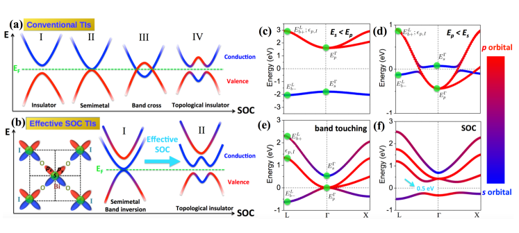
In this work, a tight-binding (TB) model of rock-salt lattice with the unit cell containing a pair of and orbitals from two atoms is proposed to implement the novel topological phase transition depicted in Figure 1(b). With such TB model, one may start with a band insulator in which the valence band is of character and the conduction band is degenerate and of character. By tuning a set of TB parameters, we are able to achieve the band structure in which the valence and conduction bands, now both having character, touch at the Fermi energy, which is protected by the cubic symmetry, and the band of character lies above them. Consequently, even with a weak SOC, the band touching at the Fermi energy is lifted at once and the highest Bloch state of valence band is of character. This flip of band character indicates the change of topological nature of the material.
More importantly, the band touching at the Fermi level and the accompanying band inversion are shown to be universal among the materials reported in this paper. Based on the first-principle calculation and Z2 index evaluation, the double perovskites A2BiXO6 (A = Ca, Sr, Ba; X = I, Br) are TI’s and the largest band gap is 0.55 eV, much larger than known pristine 3D TIs. Further confirmation by employing the Wannier function-based tight-binding calculation allows us to see the Dirac spectrum of the surface states. Since perovskites are stable materials with variable properties by doping, the reported materials could add to the already diverse functionality of perovskites which has been intensively studied. 37, 38, 39, 40, 41, 42, 43, 44
Band touching in the known materials, graphene for instance, often implies some discrete symmetry from the lattice 15. Here, we introduce a generic tight-binding model for rock-salt lattice from which a band touching at point emerges if the band energies at and around the Fermi level are ordered according to Eq. 15. Here, we consider the Bi and I atoms with each contributing one -orbital and three -orbitals. Dictated by the cubic symmetry, the tight-binding Hamiltonian in momentum space reads
| (5) |
in the representation of the eight atomic orbitals, . The spin is suppressed for the moment, and each element in the matrix is in fact a two-by-two matrix. The diagonal ones read
| (8) |
and
| (11) |
which are responsible for the coupling between orbitals from different atoms but of the same symmetry. For shorter notation, the sum in the off-diagonal element of reads . Similar expressions in and can be inferred from the cubic symmetry. The and -orbitals are coupled by the off-diagonal matrices, with , and being the first of three Pauli matrices. In the followings, we assume the order of orbital energies: . Besides, the Fermi level is above the second lowest band and below the third lowest band of the matrix in Eq. 5.
At point all the matrices vanish identically. Thus, one easily identifies the higher -like state,
| (12) |
out of (Eq. 8), which is close to the Fermi level. Similarly, the lower -like states,
| (13) |
are obtained from and are triply degenerate due to the cubic symmetry. The states away from these levels are not relevant to the band touching. At the point, it is less straightforward to obtain the band energies. Nevertheless, we show in the Supplemental Material that the eigenvalues contain two doublets at and , respectively, and four nondegenerate states at and as a result of - mixings. It will be clear in a moment that the states,
| (14) |
close to the Fermi level are relevant to the formation of band touching at the point. Here, it should be noticed that due to the rock-salt lattice geometry all the hopping parameters , , and appear in the off-diagonal part of Eq. 5 so the band energy is invariant under the mapping , the robustness of which is not present in other models. 41, 43
At the outset, the band structure may represent a trivial insulator [Figure 1(c)] in which the higher band is below the lower band and the Fermi level lies between them. This situation, , occurs if the hopping is weak and the on-site energies have . As we lift toward , the band at can be above the band [Figure 1(d)] once the condition is satisfied. To make a hole band emerge in the presence of the triple degeneracy at , the only way is to increase so that the energy is pushed down below . Finally, the crossing of bands at the Fermi level is established [Figure 1(e)] under the following condition,
| (15) |
and, remarkably, the band character is inverted simultaneously. Now the only missing element is a energy gap at the Fermi level so we follow by restoring the spin degree of freedom and turning on the SOC in the form , which leads to the gap opening at in Figure 1(f). Aided by the color code in Figure 1(c)-(f) representing the weight of character of the corresponding Bloch state, one can notice a complete topological phase transition from (c) to (f). Focus on the point. Since the Bloch state just below the Fermi level changes from the character in (c) to the character in (f), we may conclude that the Z2 invariant 51 associated with Figure 1(c) and (f) must be different and hence the two states must represent distinct phases. In the followings, we shall specifically focus on the double perovskites and show that the above tight-binding model is essential to their band structure and topological property.
Before entering the detailed calculations of real materials, let us pause and compare the TB model in Eq. 5 with the well-known BHZ model. 5 The latter is a continuum one obtained by projection and has two important ingredients in it, namely the inversion of conduction versus hole bands and the coupling that depends linearly on the crystal momentum. These two crucially depend on the SOC of constituents. In our model, however, it is the tuning of which results in the hole band and the band touching at point simultaneously. The inversion of band in our model has nothing to do with SOC, either. Moreover, the SOC that couples the electron band with the hole band does not depend on the crystal momentum. Thus, the present model is qualitatively different from the BHZ model.
The class of materials A2BiXO6 in double perovskite structure is shown in the Figure 2(a) and its primitive Brillouin zone in Figure 2(b). The unit cell contains the octahedra BiO6 and XO6 at the corners of rock-salt lattice and the cation A is surrounded by these octahedra. Determined by the electron negativity of the constituent, the charge state in the ionic limit can be assigned as: A2+, Bi3+, X5+, and O2-. Using the first-principles package VASP 45 with generalized gradient approximation (GGA) for the correlation functional 46, projector augmented wave method (PAW) for core electrons 47, for k-sampling integration 48 and 500eV for energy cutoff, we find a total of six TIs out of a large number of possible double perovskites (Ca,Sr,Ba)2BB’O6 with B and B’ from the III to VII families. The optimized lattice parameters and the band gaps with SOC are listed in Table 1.
| Compound | a=b=c() | (eV) | |
|---|---|---|---|
| Ba2BiIO6 | 6.241 | 60 | 0.55 |
| Sr2BiIO6 | 6.169 | 60 | 0.53 |
| Ca2BiIO6 | 6.123 | 60 | 0.52 |
| Ba2BiBrO6 | 6.102 | 60 | 0.33 |
| Sr2BiBrO6 | 6.009 | 60 | 0.32 |
| Ca2BiBrO6 | 5.951 | 60 | 0.34 |
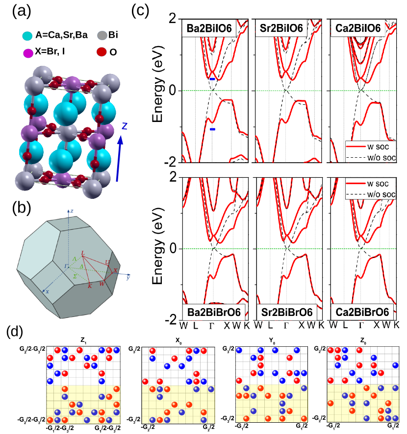
Figure 2(c) shows the band structures of the six TIs A2BiXO6. The band structures barely change as the A-site elements vary. However, the band gap is sensitive to the choice of X. Since the SOC is weaker in Br than in I, the band gap in the materials with Br is only 60 of those with I. A key feature of these band structures is the band touching at the -point in the absence of SOC. Clearly, the triple degeneracy is resolved into a doublet and a singlet in the presence of SOC, which is consistent with the previous TB model.
To examine the topological feature of these materials, we implement the n-field method of evaluating the Z2 invariant proposed by Fukui et. al. 49, 50. The resultant n-field diagrams of a representative material Ba2BiIO6 are shown in Figure 2(d). We found that the six materials share the same Z2 invariants (; ) = (1; 0 0 0), indicating that all the six materials are strong TIs. On the other hand, Fu and Kane proposed another method to obtain the Z2 invariant for crystals with inversion symmetry by evaluating the parity eigenvalues of the occupied bands 51. Table 2 displays the invariant associated with the full set of occupied bands of Ba2BiIO6 at the eight time-reversal invariant momenta (TRIM) as well as the parity eigenvalues () of the band just below (above) the Fermi level. We thus obtain the same topological invariant (; ) = (1; 0 0 0), consistent with the n-field method.
| – | – | – | + | – | + | + | – | |
| – | + | + | – | + | – | – | + | |
| – | – | – | + | – | + | + | – |
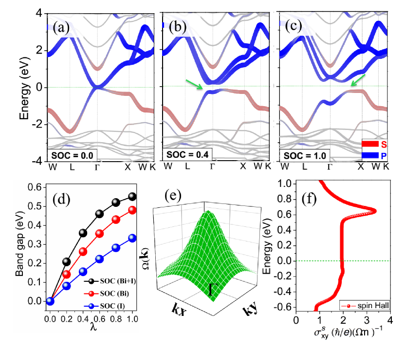
Next, we continue with studying the band characters near the Fermi level. The respective weight of - and -components of the Bloch states are calculated by DFT and are shown by the color code in Figure 3 in which the SOC is gradually turned on to its full strength. In the case of vanishing SOC [Figure 3(a)], the lowest conduction band is composed of -orbitals only while the highest valence band has the main component from -orbitals except near the point. From the aspect of Z2 invariant, one may regard this state as a TI with zero band gap. According to Figure 3(b) and (c), as the SOC is gradually turned on, the size of band gap increases accordingly while the band character remains, eventually leading to a large band gap [Figure 3(d)]. It is important to note that the SOC in this class of materials does not serve to exchange the band character, or the parity eigenvalue, unlike what it does in conventional TI Bi2Se3. To further clearly identify the non-trivial topology, we also calculate the spin Berry curvature [Figure 3(e)] associated with the occupied band and the resultant spin Hall conductance [Figure 3(f)] as a function of Fermi energy. The quantized values of spin Hall conductance within the SOC gap demonstrates the critical features of the topological phase.
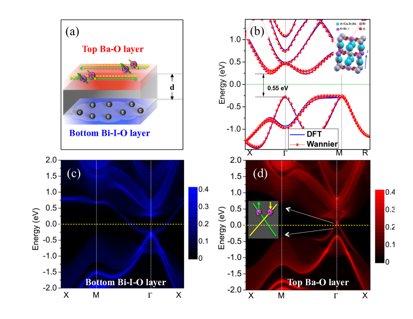
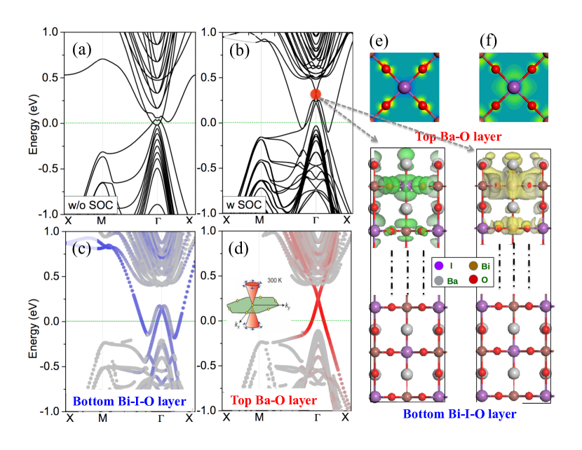
Another benchmark of a TI is the presence of linear dispersion within the bulk gap representing the Dirac electron on the surface. To investigate the surface states, we consider the semi-infinite slab structure with two types of surface. The one at top is terminated at the Ba-O layer while the one at bottom is at Bi-I-O layer, which is shown in Figure 4(a). A tight-binding Hamiltonian is constructed with the maximally localized Wannier functions (MLWFs) using WANNIER90 package 52. The bulk band structures from MLWF are shown in Figure 4(b), showing excellent agreement comparing to DFT bands. The surface spectral weight of the semi-infinite slab is computed by the surface Green’ s function method 53, 54, 55. Surprisingly, as shown in Figure 4(c), a non-Dirac-like dispersion appears at the bottom Bi-I-O layer at which dangling bonds present. Since the Bloch states around the Fermi level have significant components falling on Bi and I atoms, the presence of dangling bond may greatly alter the wavefunctions and the surface states. On the other hand, as shown in Figure 4(d), a Dirac-like spectrum is clearly presented on the top surface terminated by Ba-O layer since the Bloch states associated with Ba are away from the Fermi energy. It is worthy mentioning that the Ba-O layer may be regarded as a cap layer that protects the Dirac state from the severe perturbation due to the dangling bond.
Although Wannier functions method is commonly used to explore the surface states, 26 it is usually considered as an artificial calculation because it uses the tight-binding parameters obtained from the bulk band structure without taking the interface effects such as surface energy renormalization and dangling bonds into account. To address this issue, we also perform the DFT calculation of a slab geometry in which 5 unit cells of Figure 2(a) are repeated along the z-axis. It corresponds to the thickness about 4 nm, which has been proven large enough against the interactions between top and bottom surfaces based on our Wannier function projected bands of analysis. The band structures of the slab geometry without and with SOC are shown in Figure 5(a) and (b), respectively. In Figure 5(c) for the bottom surface, a distorted in-gap Dirac spectrum state emerges around the -point. This distorted Dirac surface states actually resemble those appear on the surface of Bi2Te3 [see Figure 8(b) in Ref. 22]. Instead, the Dirac state on the top surface [Figure 5(d)] is more transparent and consistent with the Wannier-function analysis in previous paragraph. According to our TB model and DFT calculation, the bulk states around the Fermi level are mainly contributed by the - and -orbitals of Bi and I atoms. When the bottom Bi-O-I layer is exposed, the dangling bonds certainly alter the states around the Fermi level, which might result in the distortion of the Dirac state. As for the case with Ba-O layer at the termination, the associated dangling bonds can only perturb the states away from the Fermi level, leaving the surface Dirac states and the Kramers doublets intact. Hence we expect the class of materials with surfaces terminated at A-O layers to possess the topological features and superior surface transport property. In fact, the Ba-O layer termination is also more structurally stable because the breaking of BiO6 or IO6 octahedra requires more energy, making the top Ba-O surface more feasible during the synthesis process. We have also plotted the 3D spatial wave functions of the pair of Dirac states [circled in Figure 5(b)] in Figure 5(e) and (f) which shows a highly localized behavior on the top second Bi-O-I layer. The 2D projections of surface wave functions clearly exhibit the - and -characters also in agreement with our previous discussion.
While the presence of robust surface Dirac states crucially distinguishes TI from the ordinary semiconductor, there could be another aspect that might differentiate the two classes from computational perspective. Namely, the GGA-PBE functionals often underestimates the band gap of semiconductors. 56 An improvement is to adopt hybrid functional such as HSE, 57 which employs a screened exchange interaction while keeping the long-ranged Coulomb interaction. It is worthwhile to stress that SOC, a relativistic effect, is the main factor in determining the band gap of the predicted TI’s. Since SOC has little to do with Hatree-Fock interaction, we believe that the adoption of HSE is irrelevant to the band gap of TI.
One distinct feature of our proposed 3D TIs is that it is intrinsic TIs with the Fermi level lying in the large non-trivial SOC gap. Synthesis of the predicted material, Ba2BiIO6 for instance, is an interesting yet challenging direction for chemists and material scientists. Currently, the compound BaBiO3 is a known superconducting material 58 while the study of solid phase of iodine oxide 59 is rare although the iodine chemistry is of importance to the research of earth ozone. 60 Besides, the predicted TI shall show robustness against disorder. For double perovskite A2BB’O6, the well-known disorder includes the self-doping, the intermixing between B and B’, and the oxygen deficiency. From our model, the intermixing may be more substantially disadvantageous since the Bloch states near the Fermi level are contributed by the B and B’ orbitals, but it can be overcome experimentally in a more controlable synthesis process. To consider another realistic situation, the robustness of TI states against surface reconstruction is investigated. As shown in Figure S1, one can see that surface relaxation mainly induces charge redistribution between the bottom and top surface from the shifting of Fermi level, leaving the main features of Dirac states unchanged. Experimentally, one can detect the topological surface states by measuring the quantized conductance protected by the topological nature, or by mapping out the surface state of solids in the reciprocal space by the state-of-art Angle-resolved photoemission spectroscopy (ARPES). Since the energy position of these surface states can be easily tuned by applying electric field, one may switch between electron and hole transport on the surfaces as well. Moreover, doping to double perovskite structure can also be implemented by replacing the A2+ cations with A1+ or A3+ ones of similar size 37, which makes the Bloch states near the Fermi level intact while little disorder is introduced to the system. Thus, the doped compounds can be converted into topological superconductor 61, 62 at sufficiently low temperature, which has immense impact on the fundamental physics of non-Abelian particles and fault-tolerant quantum computations 63. We believe that our work may provide an interesting platform and stimulate new experimental investigations of double-pervoskite structures in many other new directions.
By proposing a generic tight-binding model for rock-salt lattice, we have shown a new notion of topological phase transition from a trivial state in Figure 1(c) to the topological state in (f) of 3D materials with strong SOC and cubic symmetry. With the band touching and band inversion in the band structure without SOC, it turns out that the SOC becomes more effective in generating a large band gap of a TI. We further suggest possible realization of our model in well-known double perovskites A2BiXO6 (A=Ca, Sr, Ba; X=I, Br) by doping V and VII elements into B and B site, with non-trivial band gap as large as 0.55eV. Further analysis on the surface states shows that the surface Dirac cone is stable on surface terminated by A and oxygen atoms and robust against surface reconstruction, providing stable TIs states for experimental realization. Our findings not only enrich the physics of TIs realm but also open a new vista of searching for new TIs in new dimensions. Our proposed materials hold great potential to realize a new paragon of 3D TIs for practical applications.
Useful conversation with M. Kennett is acknowledged. Work at National Taiwan Normal University was supported by Taiwan Ministry of Science and Technology through Grant No. 103-2112-M-003-012-MY3 and No. 103-2112-M-003-005. Work at University of California, Irvine was supported by DOE-BES (Grants No. DE-FG02-05ER46237 for H.W. and No. SC0012670 for S.P.). Computer simulations were partially supported by NERSC and National Center for High-Performance Computing of Taiwan.
Supporting Information. Derivation of the band energy in Eq. 14 and surface band structure considering the presence of dangling bond included.
References
- 1 von Klitzing, K.; Dorda, G; Pepper, M. New Method for High-Accuracy Determination of the Fine-structure Constant Based on Quantized Hall Resistance. Phys. Rev. Lett. 1980, 45, 494.
- 2 Haldane, F. D. M. Model for a Quantum Hall Effect without Landau Levels: Condensed-matter Realization of the “Parity Anomaly”. Phys. Rev. Lett. 1988, 61, 2015.
- 3 Kane, C. L.; Mele, E. J. Quantum Spin Hall Effect in Graphene. Phys. Rev. Lett. 2005, 95, 226801.
- 4 Bernevig, B. A.; Zhang, S.-C. Quantum Spin Hall Effect. Phys. Rev. Lett. 2006, 96, 106802.
- 5 Bernevig, B. A.; Hughes T. L.; Zhang, S.-C. Quantum Spin Hall Effect and Topological Phase Transition in HgTe Quantum Wells. Science 2006, 314, 1757-1761.
- 6 Oka, T.; Aoki, H. Photovoltaic Hall Effect in Graphene, Phys. Rev. B 2009, 79, 106802.
- 7 Linder, N. H.; Rafel, G.; Galitski, V. Floquet Topological Insulator in Semiconductor Quantum Wells, Nat. Phys. 2011, 7, 490-495.
- 8 Pi, S.-T.; Savrasov, S. Y. Polarization Induced Z2 and Chern Topological Phases in a Periodically Driving Field. Sci. Rep. 2016, 6, 22993.
- 9 Fu, L. Topological Crystalline Insulators. Phys. Rev. Lett. 2011, 106, 106802.
- 10 Wang, Z.; Sun, Y.; Chen, X.-Q.; Franchini, C.; Xu, G.; Weng, H.; Dai, X.; Fang, Z. Dirac Semimetal and Topological Phase Transitions in A3Bi (A=Na, K, Rb). Phys. Rev. B 2012, 85, 195320.
- 11 Wang, Z.; Weng, H.; Wu, Q.; Dai, X.; Fang, Z. Three-dimensional Dirac Semimetal and Quantum Transport in Cd3As2. Phys. Rev. B 2013, 88, 125427.
- 12 Wan, X.; Turner, A. M.; Vishwanath, A.; Savrasov, S. Y. Topological Semimetal and Fermi-arc Surface States in the Electronic Structure of Pyrochlore Iridates. Phys. Rev. B 2011, 83, 205101.
- 13 Xu, S.-Y.; Belopolski, I.; Alidoust, N.; Neupane, M.; Bian, G.; Zhang, C.; Sankar, R.; Chang, G.; Yuan, Z.; Lee, C.-C.; et al. Discovery of a Weyl Fermion Semimetal and Topological Fermi Arcs. Science 2015, 349, 613-617.
- 14 Thouless, D. J.; Kohmoto, M.; Nightingale, M. P.; den Nijs, M. Quantized Hall Conductance in a Two-dimensional Periodic Potential. Phys. Rev. Lett. 1982, 49, 405.
- 15 Schnyder, A. P.; Ryu, S.; Furusaki, A; Ludwig, A. W. W. Classification of Topological Insulators and Superconductors in Three Spatial Dimensions. Phys. Rev. B 2008, 78, 195125.
- 16 Yang B.-J.; Nagaosa, N. Classification of Stable Three-dimensional Dirac Semimetals with Nontrivial Topology. Nat. Commun. 2014, 5, 4898.
- 17 Fu L.; Kane, C. L. Superconducting Proximity Effect and Majorana Fermions at the Surface of a Topological Insulator. Phys. Rev. Lett. 2008, 100, 096407.
- 18 Qi, X.-L.; Li, R.; Zang, J.; Zhang, S.-C. Inducing a Magnetic Monopole with Topological Surface States. Science 2009, 323, 1184-1187.
- 19 Checkelsky, J. G.; Ye, J.; Onose, Y.; Iwasa, Y.; Tokura, Y. Dirac-fermion-mediated Ferromagnetism in a Topological Insulator. Nat. Phys. 2012, 8, 729-733.
- 20 Zhang, J.; Chang, C.-Z.; Tang, P.; Zhang, Z.; Feng, X.; Li, K.; Wang, L.-L.; Chen, X.; Liu, C.; Duan, W.; et al. Topology-driven Magnetic Quantum Phase Transition in Topological Insulators. Science 2013, 339, 1582-1586.
- 21 Hasan, M. Z.; Kane, C. L. Colloquium: Topological Insulators. Rev. Mod. Phys. 2010, 82, 3045.
- 22 Ando, Y. Topological Insulator Materials. J. Phys. Soc. Jpn. 2013, 82, 102001.
- 23 Hor, Y. S.; Richardella, A.; Roushan, P.; Xia, Y.; Checkelsky, J. G.; Yazdani, A.; Hasan, M. Z.; Ong, N. P.; Cava, R. J. -type Bi2Se3 for Topological Insulator and Low-temperature Thermoelectric Applications. Phys. Rev. B 2009, 79, 195208.
- 24 Xu, Y.; Gan, Z.; Zhang, S.-C. Enhanced Thermoelectric Performance and Anomalous Seebeck Effects in Topological Insulators. Phys. Rev. Lett. 2014, 112, 226801.
- 25 Pal, K.; Anand, S.; Waghmare, U. V. Thermoelectric Properties of Materials with Nontrivial Electronic Topology. J. Mater. Chem. C 2015, 3, 12130-12139.
- 26 Zhang, H.; Liu, C.-X.; Qi, X.-L.; Dai, X.; Fang, Z.; Zhang, S.-C. Topological Insulator in Bi2Se3, Bi2Te3, and Sb2Te3 with a Single Dirac Cone on the Surface. Nat. Phys. 2009, 5, 438-442.
- 27 Kushwaha, S. K.; Pletikosic, I.; Liang, T.; Gyenis, A.; Lapidus, S. H.; Tian, Y.; Zhao, H.; Burch, K. S.; Lin, J.; Wang, W.; et al. Sn-doped Bi1.1Sb0.9Te2S Bulk Crystal Topological Insulator with Excellent Properties. Nat. Commun. 2016, 7, 11456.
- 28 Hu, J.; Alicea, J.; Wu, R. Q.; Franz, M. Giant Topological Insulator Gap in Graphene with 5 Adatoms. Phys. Rev. Lett. 2012, 109, 266801.
- 29 Ma, Y.; Dai, Y.; Niu, C.; Huang, B. Halogenated Two-dimensional Germanium: Candidate Materials for Being of Quantum Spin Hall State. J. Mater. Chem. 2012, 22, 12587-12591.
- 30 Xu, Y.; Yan, B.; Zhang, H.-J.; Wang, J.; Xu, G.; Tang, P.; Duan, W.; Zhang, S.-C. Large-gap Quantum Spin Hall Insulators in Tin Films. Phys. Rev. Lett. 2013, 111, 136804.
- 31 Zhou, M.; Ming, W.; Liu, Z.; Li, P.; Liu, F. Epitaxial Growth of Large-gap Quantum Spin Hall Insulator on Semiconductor Surface. PNAS 2014, 111, 14378-14381.
- 32 Wang, H.; Pi, S.-T.; Kim, J.; Wang, Z.; Fu, H. H.; Wu, R. Q. Possibility of Realizing Quantum Spin Hall Effect at Room Temperature in Stanene/Al2O3(0001). Phys. Rev. B 2016, 94, 035112.
- 33 Murakami, S. Phase Transition Between the Quantum Spin Hall and Insulator Phases in 3D: Emergence of a Topological Gapless Phase. New J. Phys. 2007, 9, 356.
- 34 Vafek O.; Yang, K. Many-body Instability of Coulomb Interacting Bilayer Graphene: Renormalization Group Approach. Phys. Rev. B 2009, 81, 041401(R).
- 35 Sun, S.; Yao, H.; Fradkin, E.; Kivelson, S. A. Topological Insulators and Nematic Phases from Spontaneous Symmetry Breaking in 2D Fermi Systems with a Quadratic Band Crossing. Phys. Rev. Lett. 2009, 103, 046811.
- 36 Yamaji Y.; Imada, M. Metallic Interface Emerging at Magnetic Domain Wall of Antiferromagnetic Insulator: Fate of Extinct Weyl Electrons. Phys. Rev. X 2014, 4, 021035.
- 37 Vasala S.; Karppinen, M. A2B’B”O6 Perovskites: A Review. Prog. Solid State Chem. 2015, 43, 1-36.
- 38 Kim, B. J.; Jin, H.; Moon, S. J.; Kim, J.-Y.; Park, B.-G.; Leem, C. S.; Yu, J.; Noh, T. W.; Kim, C.; Oh, S.-J.; et al. Novel = 1/2 Mott State Induced by Relativistic Spin-orbit Coupling in Sr2IrO4. Phys. Rev. Lett. 2008, 101, 076402.
- 39 Kojima, A.; Teshima, K.; Shirai, Y.; Miyasaka, T. Organometal Halide Perovskites as Visible-light Sensitizers for Photovoltaic Cells. J. Am. Chem. Soc. 2009, 131, 6050-6051.
- 40 Burschka, J.; Pellet, N.; Moon, S.-J.; Humphry-Baker, R.; Gao, P.; Nazeeruddin, M. K.; Gratzel, M. Sequential Deposition as a Route to High-performance Perovskite-sensitized Solar Cells. Nature 2013, 499, 316-319.
- 41 Jin, H.; Im, J.; Freeman, A. J. Topological Insulator Phase in Halide Perovskite Structures. Phys. Rev. B 2012, 86, 121102(R).
- 42 Jin, H.; Rhim, S. H.; Im, J.; Freeman, A. J. Topological Oxide Insulator in Cubic Perovskite Structures. Sci. Rep. 2013, 3, 1651.
- 43 Yan, B.; Jasen, M.; Felser, C. A Large-energy-gap Oxide Topological Insulator Based on the Superconductor BaBiO3. Nat. Phys. 2103, 9, 709-711.
- 44 Yang, M.; Wang, R. N. Topological Insulator in Tellurium-based Perovskites, Int. J. Mod. Phys. B 2015, 29, 1550073.
- 45 Kresse, G.; Hafner, J. Ab initio Molecular-dynamics Simulation of the Liquid-metal-amorphous-semiconductor Transition in Germanium. Phys. Rev. B 1994, 49, 14251.
- 46 Perdew, J. P.; Burke, K.; Ernzerhof, M. Generalized Gradient Approximation Made Simple. Phys. Rev. Lett. 1996, 77, 3865.
- 47 Kresse, G.; Joubert, D. From Ultrasoft Pseudopotentials to the Projector Augmented-wave Method. Phys. Rev. B 1999, 59, 1758.; Blochl, P. E. Projector augmented-wave method. Phys. Rev. B 1994, 50, 17953.
- 48 Monkhorst, H. J.; Pack, J. D. Special Points for Brillouin-zone Integrations. Phys. Rev. B 1976, 13, 5188.
- 49 Fukui, T.; Hatsugai, Y.; Suzuki, H. Chern Numbers in Discretized Brillouin Zone: Efficient Method of Computing (Spin) Hall Conductances. J. Phys. Soc. Jap. 2005, 74, 1674-1677.
- 50 Fukui T.; Hatsugai, Y. Quantum Spin Hall Effect in Three Dimensional Materials: Lattice Computation of Z2 Topological Invariants and Its Application to Bi and Sb. J. Phys. Soc. Jap. 2007, 76, 053702.
- 51 Fu, L.; Kane, C. L. Topological Insulators with Inversion Symmetry. Phys. Rev. B 2007, 76, 045302.
- 52 Mostofi, A. A.; Yates, J. R.; Pizzi, G.; Lee, Y. S.; Souza, I.; Vanderbilt, D.; Marzari, N. An Updated Version of Wannier90: A Tool for Obtaining Maximally-Localised Wannier Functions. Comput. Phys. Commun. 2014, 185, 2309-2310.
- 53 Sancho, M. P. L.; Sancho, J. M. L.; Rubio, J. Quick Iterative Scheme for the Calculation of Transfer Matrices: Application to Mo (100). J. Phys. F: Met. Phys. 1984, 14, 1205-1215.
- 54 Sancho, M. P. L.; Sancho, J. M. L.; Sancho, J. M. L.; Rubio, J. Highly Convergent Schemes for the Calculation of Bulk and Surface Green Functions. J. Phys. F: Met. Phys. 1985, 15, 851.
- 55 Lee P.; Kim, J.; Kim, J.; Ryu, M.; Park, H.; Kim, N.; Kim, Y.; Lee, N.; Kioussis, N.; Jhi, S.; et al. Topological Modification of the Electronic Structure by Bi-bilayers Lying Deep Inside Bulk Bi2Se3. J. Phys.: Condens. Matter 2016, 28, 085002.
- 56 Zhao, Y.; Truhlar, D. G. Calculation of Semiconductor Band Gaps with the M06-L Density Functional, J. Chem. Phys. 2009, 130, 074103.
- 57 Heyd, J.; Scuseria, G. E.; Ernzerhof, M. Hybrid Functional Based on a Screened Coulomb Potential, J. Chem. Phys. 2004, 118, 8207-8215.
- 58 Sleight, A. W.; Gillson, J. L.; Bierstedt, P. E. High Temperature Superconductivity in the BaPb1-xBixO3 Systems. Solid State Commun. 1975, 17, 27-28.
- 59 Nikitin, I. V. Halogen Monoxides, Russ. Chem. Rev. 2008, 77, 739-749.
- 60 Saiz-Lopez, A.; Fernandez, R. P.; Ordonez, C.; Kinnisons, D. E.; Gomez Martin, J. C.; Lamarque, J.-F.; Tilmes, S. Iodine Chemistry in the Troposphere and its Effect on Ozone, Atoms. Chem. Phys. 2014, 14, 13119-13143.
- 61 Hor, Y. S.; Williams, A .J.; Checkelsky, J. G.; Roushan, P.; Seo, J.; Xu, Q.; Zandbergen, H. W.; Yazdani, A.; Ong, N. P.; Cava, R. J. Superconductivity in CuxBi2Se3 and its Implications for Pairing in the Undoped Topological Insulator. Phys. Rev. Lett. 2010, 104, 057001.
- 62 Fu, L.; Berg, E. Odd-Parity Topological Superconductors: Theory and Application to CuxBi2Se3. Phys. Rev. Lett. 2010, 105, 0097001.
- 63 Ivanov, D. A. Non-Abelian Statistics of Half-Quantum Vortices in -Wave Superconductors. Phys. Rev. Lett. 2001, 86, 268.