Effects of the Substitutions and Vacany Defects on the Stable monolayer structures of Black and Blue Arsenic Phosphorus: A First Principles Study
Abstract
We investigate two dimensional monolayer structures of arsenic phosphorus ( AsP) by means of first principles plane wave method within density functional theory using the generalized gradient approximation. Two structures of arsenic phosphorus are taken into account which are called buckled (B-AsP) and puckered (Pu-AsP). From our numerical calculations we predicted the optimized states of a single-layer buckled and puckered honeycomb like allotropes of AsP. We demonstrate that buckled and puckered arsenic phosphorus are semiconducting single layers with band gap energies 1.858 eV and 0.924 eV, respectively. Especially, we have found that the puckered monolayer has a direct band gap. Furhermore, we examined the electronic and magnetic properties of various kind of point defects including single and double vacancies, antisite and substitutions on both buckled and puckered arsenic phosphorus. We conclude that AsP monolayers can attain magnetic state with vacancies and the semiconductor nature can turn into metal with diverse defect types. In considered system also the band gap of B-AsP can be tuned from metal character to 1.858 eV and for Pu-AsP from metal to 0.924 eV which these ranges are especially important for radar and atmosferic applications.
pacs:
71.15.Mb \sep73.20.At \sep73.22.-f \sep73.90.+f \sep75.70.AkI Introduction
The two dimensional monolayer honeycomb structures have exceptional properties and thus attracted a growing interest with theirs promising applications in nanotechnology. Recent studies in nanoscale physics have aimed the discovering new monolayer materials and revealing their properties under different conditions. Among these materials, graphene, which is a single layer honeycomb structure of carbon, has attracted great interest in various fields ranging from electronics to biotechnology due to its unique properties, such as high mechanical strenght, chemical stability, and exceptional ballistic conductance Geim ; Novoselov . The search for the contender of graphene has led to the prediction/synthesis of new single-layer, crystalline nanostructures, which do not exit in nature. Silicene, germanene, stanene, namely graphene analogs of group IV or V elements Durgun ; Cahangirov ; Vogt ; Ozcelik ; Xu ; h-BN analogs of group IV-IV, III-V, and II-VI compounds Sahin ; graphyne Tongay ; Malko ; Ozcelik2 and the auxetic piezoelectric 2D material silicatene with negative Poissons ratio Ozcelik3 ; Xu2 have been actively studied. Additionally, transition-metal dichalcogenides have proven to be superior than graphene in specific optoelectronic applications Joensen ; Coleman ; Ataca1 ; Ataca2 . Especially, the silicene and germanene Cahangirov have attained significant interest due to their nonmagnetic semimetallic behavior with linearly crossing and bands at Fermi level which is similar to graphene and due to their compatibility with silicon-based micro-electronic industry. In addition, two dimensional silicon carbide (SiC) and germanium carbide (GeC) honeycomb structures have been reported theoretically as stable Bekaroglu ; Sahin ; Sun ; Xu3 . However, the electronic structure of graphene, and silicene, germanene as well have zero band gap, which restrain the ability and applications of them.
More recently, the fabrication of field effect transistors using micrometer-sized flakes consisting of two and three layers of black phosphorus Li and their theoretical analysis Zhu ; Low revealing the stability of its single-layer allotropes brought group V elements into the focus. In contrast to the zero band gap of honeycomb lattices of group-IV elements, monolayer honeycomb structures of group-V elements such as Phosphorene PRL , Arsenene PRBarsenene and Antimonene PRBakturk are direct and indirect band gap semiconductors, respectively and they were found as stable PRL ; PRBarsenene ; PRBakturk and the mechanical and electronic AngeChemie properties were investigated. Because of direct or indirect band gap properties, these honeycomb monolayer structures can be promising materials for digital circuits and light-emitting diodes.
To date, these 2D layered materials have covered a wide electromagnetic spectral range including metals, semimetals, semiconductors, and insulators. Specifically, monolayer graphene is a semimetal which exhibits a zero band gap in its natural states and strong electrical field can be used in order to create a band gap in bilayer graphene Zhang . Few-layer and/or monolayer structures of group V elements, including phosphorene and arsenene, are emerging as promising candidates for two-dimensional (2D) electronic materials application Narita ; Maruyama ; Liu ; Zhu2 ; Liu2 . Different from semimetallic graphene, these systems display a nonzero band gap while still maintaining a relatively high carrier mobility Zhang2 ; Koenig ; Gomez ; Xia . One of the newest members of the 2D layered material family is black phosphorus, which is a semiconductor exhibiting a moderate band gap of around 0.3 eV in its bulk form and up to 2.2 eV as in a monolayer Wang , further pushing the band gap of single layered materials to the middle-wavelength infrared regime. Therefore, a broad spectral range has now been covered by the above mentioned layered materials. Although a wide range in electromagnetic spectrum has been covered by these 2D monolayer materials, there is still a big need to different smart materials because of the light radars and atmosferic applications in the longwavelength spectrum range. On the other hand, because of its direct band gap, black phosphorus is currently considered the best material on-chip dedectors. Besides all of these advantages, few-layer black phosphorus samples demonstrate high reactivity, resulting in a fast degradation of crystals under ambient conditions and while being chemically much less reactive, layered gray arsenic also display a significant band gap. In order that reason, the combination of black phosphorus and gray arsenic may exhibit phase coexistence that should bring an unexpected richness in both structural and electronical properties, in comparison to pristine of phosphorene and arsenene, has already been shown by the end of year 2015 Tomanek . This structure has been called black arsenic phosphorus and the honeycomb structure which can also be exist in nature is called blue arsenic phosphorus.
Although both buckled and puckered arsenene monolayers are stable structures which are shown by phonon spectrums and with theirs cohesive energies, they possess indirect band gaps of 0.831 eV and 1.635 eV, respectively PRBarsenene . In this paper, motivating by recent studies of phosphorene and arsenene, our aim is modifying the indirect gap of arsenene by making black arsenic phosphorus or in other words by substitution of arsenic atoms to phosphorene. Additionally, we are thinking that the electronic properties of these new phases of arsenic phosphorus can be tuned further and can be functionalized by substitution and vacany processes. Because previous experimantal and theoretical studies have proven that bare 2D monolayer structures can be functionalized through point defects to attain crucial physical and chemical properties for diverse applications.
On this object, we present ab initio calculations of the arsenic phosphorus allotropes in the frame of first principles calculations. Beside Si, Ge, Sn monolayers and with the development of experimental technology, AsP monolayer have the advantage of manufacturing by exfoliating crystalline black phosphorus which has been shown recently by Liu et. al. Adv.Mat.2015 . In this study, a new synthetic route was used for the synthesis of AsP layers which uses gray arsenic and red phosphorus as starting materials. Therefore AsP is chosen as the research objective of interest here. We investigate the stability and electronic properties of the 2D honeycomb structures. We have found that two honeycomb structures called buckled (B-AsP) and puckered (Pu-AsP) arsenic phoshporus are stable and the puckered AsP structure has a direct band gap. Furthermore we focus on investigating the effects of the point defects in the physical properties of black and blue arsenic phosphorus monolayers by first principles calculations. In all structures the geometric optimization are done and the recontruction, the effects on the electronic properties have been discussed. In summary, the works discussed in this letter may open a new page in the field of material science by predicting new “smart surfaces”.
The rest of the paper is organized as follows. In Section II the calculation methods are described in detail. Then, Section III contains the results and discussion. Finally, Section IV concludes the paper with a summary of our findings.
II Calculation Methods
The structural stability and the electronic properties of the Arsenic Phosphorus monolayer structures have been investigated by means of first-principles plane-wave calculations within density functional theory (DFT) using projector augmented wave (PAW) potentials paw . The exchange-correlation potential is approximated by generalized gradient approximation (GGA) using Perdew-Burke-Ernzerhof (PBE) parametrization pbe . All numerical results have been obtained by using Quantum Espresso software pwscf . A plane-wave basis set with the kinetic energy cutoff 65 Ry is used. Pseudopotentials with and valence electron configurations for As and P atoms were used, respectively. All structures are treated using periodic boundary conditions.
The Brillouin zone has been sampled by (21211) and (771) special mesh points in k-space by using Monkhorst-Pack scheme monk for (11) and (44) AsP cells, respectively. All atomic positions and lattice constants are optimized by using BFGS quasi-Newton algorithm BFGS where the total energy and forces are minimized. The convergence criteria for energy is chosen as Ry between two consecutive steps. The maximum Hellmann-Feynman forces acting on each atom is less than 0.001 Ry/au upon ionic relaxation. The maximum pressure on the unit cell is less than 0.5 kbar. Gaussian type Fermi-level smearing method is used with a smearing width of 0.1 eV.
III Results and discussion
III.1 Structural properties of the monolayers
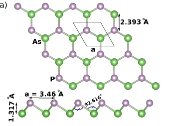
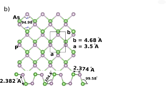
Graphene is a planar honeycomb structure since it form pure hybridization. On the other hand except graphene the other elemental honeycomb monolayers form buckled structures for example the silicene and germanene are the most popular ones. In addition, which has recently predicted, the phosphorene made of black phosphorus has a puckered structure and its buckled structure namely blue phosphorus has been investigated by first principles study PRL . From this purpose, we take two structures of arsenic phosphorus into account and show the optimized geometric structures for the cases a) buckled b) puckered in Fig.1 from side view and from top view. The structural parameters corresponding to the two different structures which are under consideration in this study are given in Table1. The lattice constants of optimized orthorhombic structure for Pu-AsP in equilibrium are and Å which are about 4 percent longer than the lattice vectors of black phosphorene and shorter than the lattice vectors of black arsenene. For the hexagonal structure B-AsP in equilibrium are Å . The B-AsP is again 4 percent longer than the blue phosphorene and shorter than blue arsenene. The bond distance between As and P atoms are Å and Å for Pu-AsP, Å for B-AsP. We found that the bond lengths of both puckered and buckled monolayers are smaller than its counterpart of arsenenes and slightly bigger than black- and blue-phosphorene.
To prove the stability of the monolayers, we calculated theirs cohesive energies defined as , where and are the total energies of single As atom, a single P atom, and a As-P pair in the AsP monolayer, respectively. The puckered and buckled monolayer structures have a cohesive energies −4,782 eV and −4,802 eV respectively per As-P pair and these values are very similar for the different monolayer structures which are stable and manufactured successfully. These values are clear evidence that AsP monolayers are strongly bonded networks. To check the structure optimizations, we increase the degrees of freedoms to 4x4 cells which we got the same geometry and cohesive energy.
In mean, we investigate here a previously unknown structure of arsenic phosphorus which called buckled structure. This structure is a honeycomb structure like graphene and it is as stable as puckered structure. Whereas these structures is hexagonal structures closely related to graphene, the main advantage of these structures are those band gaps which are approximately in the range of 1.0 - 2.0 eV. Although the band gaps are typically underestimated with the DFT calculations from the literature the general trend is confirmed, and the black- and blue arsenic phosphorus have larger band gaps than the 2D counterparts where aditionally the puckered structure has the advantage of direct band gap. Because the band gaps of most explored 2D materials exhibite moderate band gaps around 0.3 eV, which greatly restricts applications based on semiconductor and optoelectronic device technology.
III.2 Electronic structure
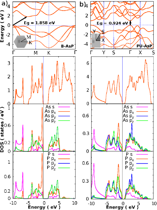
Here we carried out the electronic band structure and in order to understand the contributions of atomic orbitals to the elctronic states we have plotted the corresponding total (DOS) and partial (PDOS) density of states for the buckled and puckered monolayers as shown in Fig.2a, Fig.2b, respectively. From the electronic band structures it is obviously seen that puckered AsP is direct band gap semiconductor with a band gap of 0.924 eV whereas buckled AsP is indirect band gap semiconductor with a band gap of 1.858 eV. It is observed from the PDOS plots that the electronic states both in puckered and buckled structures have contributions from and orbitals near the Fermi energy, but the orbital contribution is very small compared to orbital contribution. This is very well known feature of monolayer honeycomb systems such as germanene, silicene and phosphorene, where the -like bonds form a nonplanar honeycomb structures different than graphene. An indirect band gap in buckled AsP resembles that of buckled (blue) phosphorene and arsenene. The valence band maximum lies at the -point, and the conduction band minimum lies along direction. Same situation are also seen both in buckled phosphorene and arsenene. Only the band gap is higher than arsenene in our case. But we could not exactly compare our value with the indirect band gap of buckled phosphorene, because its band gap was given as approximate value PRL . On the other hand, the direct gap semiconducting behaviour of puckered AsP is distincly different from the indirect band gap behaviour of puckered arsenene. Its looks like mostly to puckered phosphorene. Because both structures have direct band gaps at the -point with band gaps of 0.91 eV for puckered phosphorene and 0.92 eV for puckered AsP, respectively. But, additionally we note that, puckered AsP structure have two seperate valence band and conduction band edges near the Fermi level. The maximum of the valence band and the minimum of the conduction band occur along direction and at the -point which both are direct edges. This fact is distincly different also from the electronic band structure of phosphorene which have only direct edge at the -point.
III.3 Investigation of the Defects structures
To investigate the effects of the defects we optimized 4x4 supercells of the buckled and puckered AsP monolayers. Such size for the supercells provide sufficient distance for the examination of the defects. As presented in Fig.1 the lattice constant and the bond length of the 4x4 supercell buckled AsP which contains 16 As and 16 P atoms, are found to be Å and Å respectively. The cohesive energy is found to be the same with the unit cell. The puckered AsP 4x4 super cell contains 32 As atoms and 32 P atoms. The lattice constants for this structure are Å and Å and the bond length is Å same with the unit cell. As illustrated in Fig.2 valance band maximum and conduction band minimum consist main contribution of p orbitals of As and P atoms near Fermi level. Single atom vacancies and antisite defects are dominate defects during the fabrication of single layer materials, or some experiment can cause these defects. The presence of these defects can change electronic and magnetic properties of the materials. We examine in this section that introducing various defects into buckled and puckered AsP monolayer can cause to crucial changes in the electronic and magnetic properties. Firstly, all defected structures are subjected to geometrical optimization and we calculated their cohesive energies which the expression is given before and formation energy for the substitution defect , where the atom Y occupies the site of atom X, by using the equation below,
.
Here, the energy for the single As and P atoms are calculated from the As-rich structure and from the P-rich structure, respectively. We take arsenene monolayer as As-rich structure and phosphorene monolayer for the P-rich structure. The considered various defects and the label of them are given as follows:
-
•
Vacancy: An atom As (P) subtract from its position in the monolayer network labelled as .
-
•
Substitution: When As(P) atom placed instead of P(As) atom labelled as .
-
•
Antisite: When the position of neighboring As and P atoms are exchanged ().
III.4 Defect Structures on B-AsP monolayer
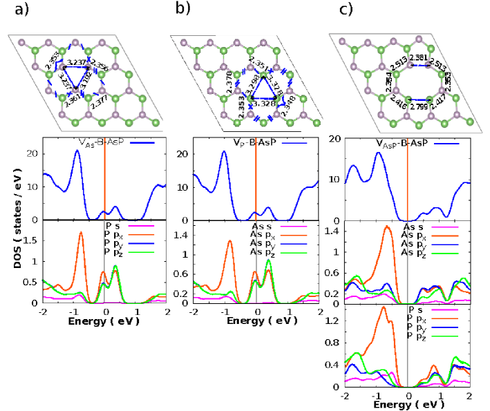
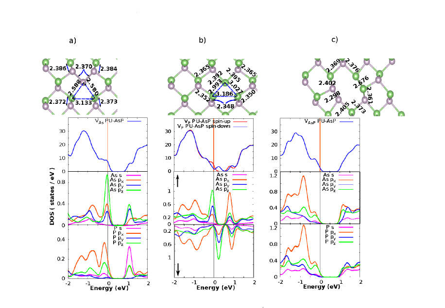
Firstly, we examine the As vacany defect structure, which the fully relaxed structure is presented in Fig.3a. After optimization, three P atoms around the vacany are approaching to each other, so the P-P distance changed to 3.237 Å and to 3.192 Å which in the pristine state was 3.460 Å. We found the bond length of As-P distance as approximately 2.361 Å which differs from the pristine monolayer while in pristine monolayer the As-P distance was 2.393 Å. The accurate structural distances are shown in figures in detail. As shown in Table2, since the cohesive energies of vacancies are almost equal, formation energy of is the highest among the others. To determine the electronic properties of the system we obtained the density of states (DOS) as presented in Fig.3a. As vacany induces a very small local magnetization (0.04 ) and the system turns to metallic character. This is the only defected state among the others on B-AsP monolayer which turns into magnetic state. As seen in Fig.3 in detail on can concluded that two defect states appear in the band gap. While one occurs from contributions of and orbitals of P atoms around the vacany, the other state at the higher energy level are mixed state of , and orbitals of P atoms around vacany. According to Löwdin charge analysis Lowdin , the excess charge on P atoms around vacany, which is calculated by substracting the charge at the atom from its valance charge, is 0.03 electrons while the other P atoms have 0.01 electrons excess charge in the bare state.
The second defected structure under consideration is P vacany () which three dangling bonds occur with As-As = 3.328 Å distance, as seen in Fig.3b. All the other bond lengths are shown in figure. This defected state is nonmagnetic and shows also metallic character. Like the case, two defect states occur at the band gap, while first consist of orbitals of As atoms around the vacany and the other has also contribution from the orbitals of the As atoms around vacany. According to Löwdin charge population analysis, As atoms around vacany gives 0.06 electrons to the surrounding substrate. Additionallyi the most energetically favourable vacany defected state is the state.
Energetically second favourable vacany defected state among the considered states is the divacany , which is the state of lacking both As and P atoms in the network. After the geometric optimization the hexagonal structure is changed to an octagon and two pentagons, which is illustrated in Fig.3c with detailed bond length informations. This is also the case where we have the biggest lattice correction with respect to the bare monolayer. The system has 0.847 eV band gap due to the defect states. As shown in Fig.3c these defects levels at around -0.75 eV and +0.70 eV have significant contributions from and orbitals. Löwdin analysis indicates that 0.10 electrons are transferred from As atoms and 0.001 electrons are transferred to P atoms around the vacany.
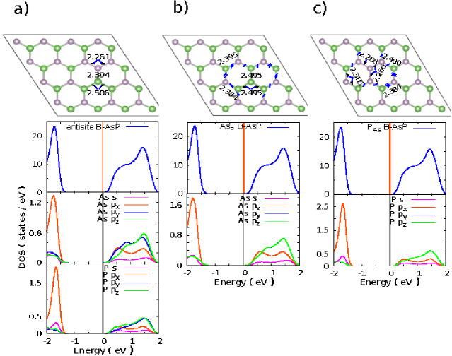
The other kind of system has antisite defect, which we exchange the positions of the neighbouring As and P atoms () in the network is presented in Fig.4a. We have detected that negligible bond length elongation occur in that system. Also there is no lattice correction. The bond length changes only from 2.393 Å to 2.394 Å. The P-P bond distance and As-As bond distance are 2.261 Å and 2.506 Å respectively. Therefore the band gap is also affected minimal only slightly from 1.858 eV to 1.831 eV. As the other cases the orbital contributions of As and P atoms around defects are shown in Fig.4a. The excess charges on the exchanged atoms are 0.11 and 0.02 electrons, respectively. These results with its small formation energy implies that this structure can be occur or dominate defect during the fabrication of AsP monolayer.
The other kind of defected is obtained by substitution of As atom instead of P atom in the monolayer (). In the fully optimized structure of (Fig.4b, four As atoms are reorganized and they bonds to each other with a bond length of As-As = 2.495 Å. The As-P bond length is nearly the same with the pristine system (2.395 Å and 2.384 Å which are denoted in the figure). There is no lattice correction. Also this defect cannot induce any magnetization and the band gap changes very slightly only to 1.804 eV. While the As atom at the central gives 0.08 electrons to the surrounding the others give 0.12 electrons.
Last considered defect for B-AsP monolayer is , the As atom is replaced by P atom in the network, is shown in Fig.4c with its optimized structure. This structure has also similar geometry with the previous defect, where the bond length of As-P is again 2.384 Å and the P-P distance is approximately 2.268 Å. Also structure is nonmagnetic and is semiconductor with a band gap 1.842 eV. In Fig.4c, we illustrate the electronic DOS of which overlaps with defect structure According to the Löwdin analysis, the central P atom has 0.16 electrons, while the other P atoms has -0.01 electrons excess charges.
III.5 Defect Structures on Pu-AsP monolayer
As in the B-AsP monolayer case, the first considered vacany defect on Pu-AsP monolayer is As vacany (), illustrated in Fig.5a. In this defect structure the lattice constants and are changed from 14.00 Å to 13.95 Å and from 18.72 Å to 18.65 Å, respectively. The bond length of As-P atoms increases from 2.395 Å to 2.580 Å. Other structural distances are shown in figure. With these structural parameters this state is one of the most defected state among the others which one can also concluded from the formation energy. To discuss the electronic properties we obtained the density of states as presented in Fig.5a. This system is nonmagnetic. The defect states occurs at the Fermi level and has contributions from both P and As atoms around the vacany. According to the Löwdin charge population analysis, the excess charge on the P atoms around the vacany is -0.03 electrons.
In the structure, we detect also lattice correction where the lattice constant are Å and Å. The accurate lengths related with the structure are given in the figure. This state is magnetic with a magnetization of 1.19 . The band gap significanly decreases from 0.924 eV to zero eV in spin-up channel while a defect state from the spin-down channel is about +0.25 eV from contributions of the orbital of As atoms around the vacany. The As atoms around the vacany gives 0.08 to the surrounding network where the other As atoms give 0.16 electrons.
The most energetically favourable state among the vacancies are the structure with a formation energy value of 0.926 eV ( Table2). After relaxation, we have found the new lattice parameters as Å and Å, respectively. The As-P bond distance is approximately 2.37 Å, where the newly constructed P-P and As-As bond distances are 2.298 Å and 2.676 Å. In distinction to the other vacany defects structures, divacany structure is nonmagnetic, with a larger band gap of 1.086 eV with respect to the bare Pu-AsP monolayer as well as with respect to the other defected structures of Pu-AsP. The defect states above and below the Fermi level has main contributions from and orbitals around the vacany. Each P (As) atom of P-P (As-As) bond has excess charge of -0.03 (0.11) electrons.
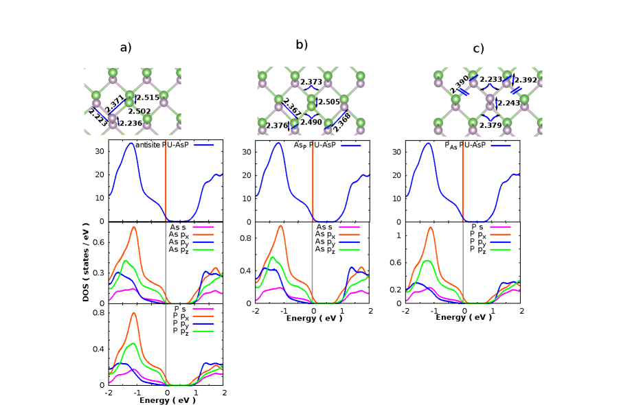
The other kind of defect considered distinctively from the vacancies is the antisite defect where the P and As atoms are exchanged (Fig.6a). We employ two different exchanging to the neighbouring P and As atoms. In the first type the exchanging is done on the x-direction and in the second one the exchanging is done on the y-direction. We detect no difference between these two defect structures at the end of the relaxation. On both system there are neither lattice constant correction nor bond distance change between the P and As atoms. These defect structures are as stable as the bare Pu-AsP monolayer structure is. The defect structures are nonmagnetic and have 0.91 eV band gaps. The exchanged atoms both give 0.06 electrons to the surrounding substrate. The formation energies are very small, so that there are no significant change due to these defect type.
Next considered defect structures are and ( As (P) atom is placed instead of P (As) atom site) where both have minimal lattice corrections (Table3) have shown in Fig.6b and c with those related bond lengths. These structures are nonmagnetic and have 0.912 eV and 0.921 eV band gaps, respectively. According to the Löwdin charge analysis, in () system the As (P) atom has excess charge of 0.03 (0.09) electrons. These defect structures have very similiar properties unlike their formation energies. From the formation energies defect is more dominate defect in comparison to defect.
IV Conclusions
In conclusion, based on the first principles plane wave calculation within the density functional theory, black and blue arsenic phosphorus monolayer structures are predicted. We show the structural and electronic properties of these monolayer structures. The black AsP monolayer is found to be a direct semiconductor with a band gap of 0.924 eV while the blue counterpart has a indirect band gap of 1.804 eV. Additionally we investigated the electronic and magnetic properties of various kind of point defects including single and double vacancies, antisite and substitutions on both puckered and buckled arsenic phosphorus. Our first principles density functional theory calculations show that the electronic and magnetic properties of pristine B-AsP and Pu-AsP monolayers can be adjustable by single and double vacancies, antisite and substition defects. The nonmagnetic semiconductor nature of both monolayes can be transformed into metallic or narrow gap semiconductor upon defected structures. The band gaps can be tuned from metal character to 1.858 eV for B-AsP and from metal to 0.924 eV for Pu-AsP which these ranges are especially important for radar and atmosferic applications. Furthermore, the vacany defects induces magnetic moments in both monolayers.
V Acknowledgement
Computing resources used in this work were provided by the TUBITAK (The Scientific and Technical Research Council of Turkey) ULAKBIM, High Performance and Grid Computing Center (Tr-Grid e Infrastructure).
References
- (1) Geim, A. K.; Novoselov, K. S. The Rise of Graphene. Nat. Mater. 2007, 6, 183-191.
- (2) Novoselov, K. S.; Geim, A. K.; Morozov, S. V.; Jiang, D.; Zhang, Y.; Dubonos, S. V.; Grigorieva, I. V.; Firsov, A. A. Science 2004, 306, 666-669.
- (3) E. Durgun, S. Tongay, and S. Ciraci, Phys. Rev. B 72, 075420 (2005).
- (4) S. Cahangirov, M. Topsakal, E. Aktürk, H. Sahin, and S. Ciraci, Phys. Rev. Lett. 102, 236804 (2009).
- (5) P. Vogt, P. Depadova, C. Quaresima, J. Avila, E. Frantzeskakis, M. C. Asensio, A. Resta, B. Ealet, and G. Lelay, Phys. Rev. Lett. 108, 155501 (2012).
- (6) V. O. Ozçelik, E. Durgun, and S. Ciraci, J. Phys. Chem. Lett. 5, 2694 (2014).
- (7) Y. Xu, B. Yan, H. J. Zhang, J. Wang, G. Xu, P. Tang, W. Duan, and S. C. Zhang, Phys. Rev. Lett. 111, 136804 (2013).
- (8) H. Sahin, S. Cahangirov, M. Topsakal, E. Bekaroglu, E. Akturk, R. T. Senger, and S. Ciraci, Phys. Rev. B 80, 155-453 (2009).
- (9) S.Tongay, S. Dag, E. Durgun, R. T. Senger, and S. Ciraci, J. Phys.: Condens. Matter 17, 3823 (2005).
- (10) D. Malko, C. Neiss, F. Vines, and A. Görling, Phys. Rev. Lett. 108, 086804 (2012).
- (11) V. O. Ozçelik and S. Ciraci, J. Phys. Chem. C 117, 2175 (2013).
- (12) V. O. Ozçelik, S. Cahangirov, and S. Ciraci, Phys. Rev. Lett. 112, 246803 (2014).
- (13) X. Xu, J. Zhuang, Y. Du, H. Feng, N. Zhang, C. Liu, T. Lei, J. Wang, M. Spencer, T. Morishita, X. Wang, and S. X. Dou, Sci. Rep. 4, 7543 (2014).
- (14) P. Joensen, R. F. Frindt, and S. R. Morrison, Mater. Res. Bull. 21, 457 (1968).
- (15) J. N. Coleman, M. Lotya, A. O. Neil, S. D. Bergin, P. J. King, U. Khan, and K. Young, Science 331, 568 (2011).
- (16) C. Ataca and S. Ciraci, J. Phys. Chem. C 115, 13303 (2011).
- (17) C. Ataca, H. Sahin, and S. Ciraci, J. Phys. Chem. C 116, 8983 (2012).
- (18) E. Bekaroglu, M. Topsakal, S. Cahangirov, S. Ciraci, Phys. Rev. B 81 (2010) 075433.
- (19) L. Sun, Y. Li, Z. Li, Q. Li, Z. Zhou, Z. Chen, J. Yang, J.G. Hou, J. Chem. Phys. 129 (2008) 174114.
- (20) B. Xu, J. Yin, Y.D. Xia, X.G. Wan, Z.G. Liu, Appl. Phys. Lett. 96 (2010) 143111.
- (21) L. Li, Y. Yu, G. J. Ye, Q. Ge, X. Ou, H. Wu, D. Feng, X. H. Chen, and Y. Zhang, Nat. Nanotechnol. 9, 372-377 (2014).
- (22) Z. Zhu and D. Tomanek, Phys. Rev. Lett. 112, 176802 (2014).
- (23) T. Low, A. S. Rodin, A. Carvalho, Y. Jiang, H. Wang, F. Xia, and A. H. Castro Neto, Phys. Rev. B 90, 075434 (2014).
- (24) Z. Zhu and D. Tomanek, Phys. Rev. Let. 112 (2014) 176802.
- (25) C. Kamal and M. Ezawa, Phys. Rev. B 91 (2015) 085423.
- (26) O. Üzengi Akturk, V. Ongun Özçelik, S. Ciraci, Phys. Rev. B 91 (2015) 234446.
- (27) S. Zhang, Z. Yan, Y. Li, Z. Chen, H. Zeng, Angew. Chem. Int. Ed. 54 (2015) 3112, 3115.
- (28) Y. Zhang , T. T. Tang , C. Girit , Z. Hao , M. C. Martin , A. Zettl , M. F. Crommie , Y. R. Shen , F. Wang , Nature 2009 , 459 , 820 .
- (29) Narita, S.; Akahama, Y.; Tsukiyama, Y.; Muro, K.; Mori, S.; Endo, S.; Taniguchi, M.; Seki, M.; Suga, S.; Mikuni, A.; Kanzaki, H. Physica B+C 1983, 117-118, 422-424.
- (30) Maruyama, Y.; Suzuki, S.; Kobayashi, K.; Tanuma, S. Physica B+C 1981, 105, 99-102.
- (31) Liu, H.; Neal, A. T.; Zhu, Z.; Luo, Z.; Xu, X.; Tomanek, D.; Ye, P. D. ACS Nano 2014, 8, 4033-4041.
- (32) Zhu, Z.; Guan, J.; Tomanek, D. Phys. Rev. B: Condens. Matter Mater. Phys. 2015, 91, 161404.
- (33) Liu, B.; Köpf, M.; Abbas, A. N.; Wang, X.; Guo, Q.; Jia, Y.; Xia, F.; Weihrich, R.; Bachhuber, F.; Pielnhofer, F.; Wang, H.; Dhall, R.; Cronin, S.; Ge, M.; Fang, X.; Nilges, T.; Zhou, C. Adv. Mater. 2015, 27, 4423-4429.
- (34) Zhang, Y.; Tan, Y. W.; Stormer, H. L.; Kim, P. Nature 2005, 438, 201-204.
- (35) S. P. Koenig, R. A. Doganov, H. Schmidt, A. H. Castro Neto and B. özyilmaz, Appl. Phys. Lett., 2014, 104, 103106.
- (36) A.Castellanos-Gomez, L. Vicarelli, E. Prada, J. O. Island, K. L. Narasimha-Acharya, S. I. Blanter, D. J. Groenendijk, M. Buscema, G. A. Steele, J. V. Alvarez, H. W. Zandbergen, J. J. Palacios and H. S. J. van der Zant, 2D Mater., 2014, 1, 025001.
- (37) F. Xia, H. Wang and Y. Jia, Nat. Commun. 2014, 5, 4458.
- (38) X. M. Wang , A. M. Jones , K. L. Seyler , V. Tran , Y. C. Jia , H. Zhao , H. Wang , L. Yang , X. D. Xu , F. N. Xia , Nat. Nanotechnol. 2015 , DOI:10.1038/nnano.2015.71.
- (39) Z. Zhu, J. Guan and D. Tomanek, Nano Lett., 2015, 15, 6042.
- (40) B. Liu, M. Kŏpf, A. Abbas, X. Wang, Q. Guo, Y. Jia, F. Xia, R. Weihrich, F. Bachhuber, F. Pielnhofer, H. Wang, R. Dhall, S. Cronin, M. Ge, X. Fang, T. Nilges, C. Zhou, Adv. Mater. 27 (2015) 4423-4429.
- (41) P.E. Blöchl, Phys. Rev. B 50 (1994) 17953.
- (42) J.P. Perdew, K. Burke, M. Ernzerhof, Phys. Rev. Lett. 77 (1996) 3865.
- (43) P. Giannozzi, S. Baroni, N. Bonini, M. Calandra, R. Car, C. Cavazzoni, D. Ceresoli, G.L. Chiarotti, M. Cococcioni, I. Dabo, A. Dal Corso, S. Fabris, G. Fratesi, S. de Gironcoli, R. Gebauer, U. Gerstmann, C. Gougoussis, A. Kokalj, M. Lazzeri, L. Martin-Samos, N. Marzari, F. Mauri, R. Mazzarello, S. Paolini, A. Pasquarello, L. Paulatto, C. Sbraccia, S. Scandolo, G. Sclauzero, A.P. Seitsonen, A. Smogunov, P. Umari, R.M. Wentzcovitch, QUANTUM ESPRESSO: A Modular and Open-Source Software Project for Quantum Simulations of Materials, J. Phys: Condens. Matter 21 (2009) 395502.
- (44) H.J. Monkhorst, J.D. Pack, Phys. Rev. B 13 (1976) 5188.
- (45) C.G. Broyden, The Convergence of a Class of Double-rank Minimization Algorithms 1. General Considerations, Journal of Institute of Mathematics and Its Applications 6 (1970) 76-90.
- (46) P.-O. Löwdin, J. Chem. Phys. 18 (1950) 365.
- (47) K. Momma, F. Izumi, VESTA 3 for three-dimensional visualization of crystal, volumetric and morphology data, J. Appl. Crystallogr. 44 (2011) 1272–1276.
Table 1: Calculated parameters for the two structures corresponding to Pu-AsP and B-AsP respectively. , the lattice constant; , As-P distance; , total energy; , band gap.
Table 2: Calculated results for optimized defective structures of B-AsP monolayer; , cohesive energy; , formation energy, , corrected lattice constant; , magnetic moment per supercell in units of Bohr magneton (NM is for nonmagnetic systems).
Table 3: Calculated results for optimized defective structures of Pu-AsP monolayer; , cohesive energy; , formation energy, and , corrected lattice constants; , magnetic moment per supercell in units of Bohr magneton (NM is for nonmagnetic systems).
Fig.1: Side view and top view of the structures of a) buckled B-AsP and b) puckered Pu-AsP.
Fig.2: Electronic band structures and corresponding density of states the for structures a) buckled B-AsP and b) puckered Pu-AsP. Zero of energy is set to Fermi level shown by dashed line. (For interpretation of the references to color in this figure legend, the reader is referred to the web version of this article.)
Fig.3: Relaxed geometries for the 4x4 supercells, the total and projected density of states plots for the defected structures on the B-AsP monolayer (a) b) c) . In DOS plots, the total DOS of pristine B-AsP monolayer and the defected structure are illustrated together for better comparison. The following orbital projected DOS plots correspond to atoms around the defect.
Fig.4: Relaxed geometries for the 4x4 supercells, the total and projected density of states plots for the defected structures on the B-AsP monolayer (a) b) c) . In DOS plots, the total DOS of pristine B-AsP monolayer and the defected structure are illustrated together for better comparison. The following orbital projected DOS plots correspond to atoms around the defect.
Fig.5: Relaxed geometries for the 4x4 supercells, the total and projected density of states plots for the defected structures on the Pu-AsP monolayer (a) b) c) . In DOS plots, the total DOS of pristine B-AsP monolayer and the defected structure are illustrated together for better comparison. The following orbital projected DOS plots correspond to atoms around the defect.
Fig.6: Relaxed geometries for the 4x4 supercells, the total and projected density of states plots for the defected structures on the Pu-AsP monolayer (a) b) c) . In DOS plots, the total DOS of pristine B-AsP monolayer and the defected structure are illustrated together for better comparison. The following orbital projected DOS plots correspond to atoms around the defect.
| Structure | (Å) | (Å) | (Å) | (eV) | (eV) | ||||
|---|---|---|---|---|---|---|---|---|---|
| 3.50 | 4.68 | 2.382 | 4.782 | 0.924 | |||||
| 3.46 | - | 2.393 | 4.802 | 1.858 |
| (eV) | 4.729 | 4.734 | 4.719 | 4.806 | 4.783 | 4.826 |
|---|---|---|---|---|---|---|
| (eV) | 2.576 | 1.708 | 2.369 | 0.140 | -0.092 | -0.084 |
| (Å) | 13.70 | 13.71 | 13.58 | 13.84 | 13.84 | 13.78 |
| 0.04 | NM | NM | NM | NM | NM |
| (eV) | 4.759 | 4.754 | 4.765 | 4.784 | 4.772 | 4.795 |
|---|---|---|---|---|---|---|
| (eV) | 1.739 | 1.336 | 0.926 | -0.115 | -0.052 | 1.336 |
| (Å) | 13.95 | 13.97 | 13.94 | 14.00 | 14.02 | 14.00 |
| (Å) | 18.65 | 18.68 | 18.64 | 18.72 | 18.74 | 18.72 |
| NM | 1.19 | NM | NM | NM | NM |