Engineering the structural and electronic phases of MoTe2 through W substitution
Abstract
MoTe2 is an exfoliable transition metal dichalcogenide (TMD) which crystallizes in three symmetries; the semiconducting trigonal-prismatic phase, the semimetallic monoclinic phase, and the semimetallic orthorhombic structure Revolins ; Vellinga ; review1 ; MoTe2_MI_transition . The phase displays a band gap of eVHeinz making it appealing for flexible and transparent optoelectronics. The phase is predicted to possess unique topological properties bernevig ; felser ; bernevig2 ; TP_transition which might lead to topologically protected non-dissipative transport channels TP_transition . Recently, it was argued that it is possible to locally induce phase-transformations in TMDs review1 ; reed1 ; reed2 ; Reed , through chemical doping phase_engineering , local heating phase_patterning , or electric-field Reed ; zhang to achieve ohmic contacts or to induce useful functionalities such as electronic phase-change memory elementsreed2 . The combination of semiconducting and topological elements based upon the same compound, might produce a new generation of high performance, low dissipation optoelectronic elements. Here, we show that it is possible to engineer the phases of MoTe2 through W substitution by unveiling the phase-diagram of the Mo1-xWxTe2 solid solution which displays a semiconducting to semimetallic transition as a function of . We find that only % of W stabilizes the phase at room temperature. Photoemission spectroscopy, indicates that this phase possesses a Fermi surface akin to that of WTe2 pletikosic .
The properties of semiconducting and of semimetallic MoTe2 are of fundamental interest in their own right, but are also for their potential technological relevance. In the mono- or few-layer limit it is a direct-gap semiconductor, while the bulk has an indirect bandgap Heinz ; Lezama ; Morpurgo_crossover of 1 eV. The size of the gap is similar to that of Si, making MoTe2 particularly appealing for both purely electronic devices MoTe2_FETs ; MoTe2_ambipolar and optoelectronic applications Mak_review . Moreover, the existence of different phases opens up the possibility for many novel devices and architectures. For example, controlled conversion of the MoTe2 phase to the phase, as recently reported park_phase_engineering , could enable circuits composed of a single material functioning as both semiconducting channels and metallic interconnects. More precise control of the phase change might also be used to minimize the metal-semiconductor Schottky barrier by continuous evolution of the electronic band structure, in order to overcome current limits on optoelectronic performance contacts . In fact, recent work has reported contact phase engineering by laser processingphase_patterning and chemical modificationphase_engineering .
.
The ability to phase-engineer MoTe2 has many broader applications and potentially deeper implications. For instance, doping, temperature, strain, and electric fields can be used to drive metal-to-insulator transitions reed1 ; Alexander ; Reed ; longo for sensors and nonvolatile information storage. More fundamentally, the electronic structure of mono-layers of semimetallic MoTe2 (and of WTe2) have been proposed to possess a topological invariant characteristic of a quantum spin Hall-effect ground-state which has a gap in the bulk and non-dissipative edge states TP_transition . If confirmed MoTe2_MI_transition , these edge states could be used for dissipation-free nano-interconnects between logical elements based on semiconducting MoTe2 for low-power electronics. More recent theoretical developments also claim that both orthorhombic MoTe2 and WTe2 would be candidates for a new type of Weyl semimetallic state characterized by linear touching points between hole- and electron-Fermi surfaces, where the Berry-phase would present topological singularities bernevig ; felser ; bernevig2 ; Weyl1 ; Weyl2 ; Hasan . These singularities, which were recently claimed to have been observed in the orthorhombic phase of MoTe2 ARPES_Huang , could lead to unconventional transport properties.
To fully control and utilize phase transitions in the two-dimensional (2D) tellurides, it is crucial to understand the phase diagram in detail. In particular, doping of the lattice can be used to precisely tune the semiconducting-metallic phase transition, and in fact W doping is known to induce a phase transition Alexander from the to an orthorhombic structure, originally identified as the phase, in Mo1-xWxTe2. Early studies identified a structural phase-transition from to for , and with a zone of phase coexistence for champion . However, given the renewed interest in this material, there is strong motivation to revisit the question of the precise evolution of the phases in the 2D tellurides with doping.
Here, we synthesize bulk crystals of Mo1-xWxTe2 alloys, and characterize their composition and structure through a combination of techniques including electron microscopy, x-ray diffraction, scanning tunneling microscopy, and Raman spectroscopy. We find that W doping produces homogeneous alloys, with no phase coexistence as previously observed champion . The structural phase transition from the semiconducting phase towards the orthorhombic and semimetallic phase is sharp and occurs at a modest critical molar fraction . Since crystals with are likely to be susceptible to small perturbations such as strain or electric field, this opens the possibility of reversibly controlling the structural, and therefore electronic properties, of the Mo1-xWxTe2 series. Additionally, we show through angle resolved photoemission spectroscopy that the geometry of the Fermi surface of Mo1-xWxTe2 is remarkably similar to that of WTe2, thus confirming its semimetallic character.
Single crystals of the Mo1-xWxTe2 series were grown through a chemical vapor transport technique as described in Methods. Unless otherwise noted, samples were cooled slowly in order to obtain the equilibrium phase at room temperature. Their precise stoichiometry was determined through energy dispersive ray spectroscopy (EDS) and photoelectron spectroscopy (XPS), see Methods as well as Supplementary Fig. S1 for photoelectron core level spectrum of a Mo1-xWxTe2 crystal and Supplementary Fig. S2 for details concerning the determination of the W content (). Stoichiometric MoTe2 () and WTe2 () were synthesized through a Te flux method. For MoTe2, samples were slowly cooled to yield the phase or quenched to room temperature to yield the metastable phase.
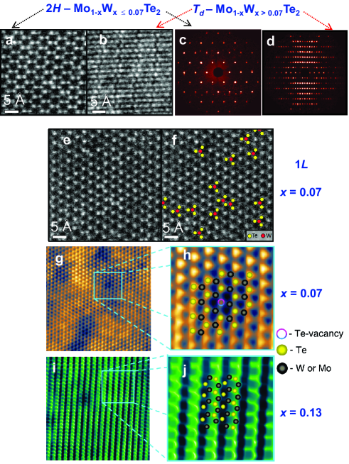
Figure 1 shows structural analysis via single crystal x-ray diffraction (XRD), scanning transmission electron microscopy (STEM), and scanning tunneling microscopy (STM). For STEM, the crystals were exfoliated following a standard procedure and transferred onto a TEM grid, see Methods. Figures 1a and 1b display atomic resolution STEM images collected from two distinct multi-layered crystals with compositions of Mo0.93W0.07Te2 and Mo0.87W0.13Te2, respectively. These crystals display distinct crystallographic structures: shows the hexagonal pattern characteristic of the trigonal prismatic or the phase, while shows a striped pattern consistent with either the or the -phase. In Supplementary Fig. S3 we have included STEM and electron diffraction images for from whose analysis we conclude that it crystallizes in the orthorhombic phase. Nevertheless, in Figs. 1c and 1d we also show single-crystal XRD patterns for and , respectively. Analysis of these patterns confirms that crystals with crystallize in the phase, whereas crystals with , in this case , display the orthorhombic phase instead of the monoclinic one. Supplementary Fig. S4 shows ray diffraction patterns for Mo0.91W0.09Te2 and Mo0.82W0.18Te2, also indicating the phase for these concentrations. Our complete set of structural studies indicate that for all concentrations , W doping stabilizes the semimetallic phase, confirming that the structural transition is sharp and occurs at a W doping level significantly lower than previously reported champion . Figure 1e shows a larger-scale STEM image of Mo0.93W0.07Te2. In this image, bright dots surrounded by three additional dots (Te atoms) correspond to randomly distributed W atoms, as highlighted in Fig. 1f. Therefore, the STEM images clearly indicate that the Mo1-xWxTe2 series results from a homogeneous dilution of W atoms into a MoTe2 matrix and not from the coexistence of MoTe2 and WTe2 domains. This lack of phase coexistence is further confirmed by room-temperature STM imaging of vacuum-cleaved crystals, as shown in Figs. 1g and 1h. For , see Fig. 1g, the equidistant distribution of Te atoms around the transition metal(s) forming an angle of among them, indicates unambiguously the trigonal prismatic coordination of the phase. In contrast, for , see Figs. 1i and 1j, rows of atoms indicate a change in symmetry from triangular to (nearly) rectangular at the surface. In amplified images, e.g. Fig. 1h, one can clearly discern Te vacancies (indicated by a multicolored dot). Therefore, we have enough resolution to observe vacancies, but we do not observe the coexistence of distinct crystallographic phases.
Thus TEM, STM, and XRD analysis yield consistent results, namely a transition from the phase to the phase at , with no phase coexistence even near the phase boundary. These observations stand in contrast to the early work in Ref. champion, , which reported a higher critical W concentration and a region of phase coexistence near the boundary. This discrepancy is likely attributable to the difference between the methods of synthesis used for each study. Having established the room temperature phase boundary between the and the transition, we now turn to the temperature axis of the phase-diagram.
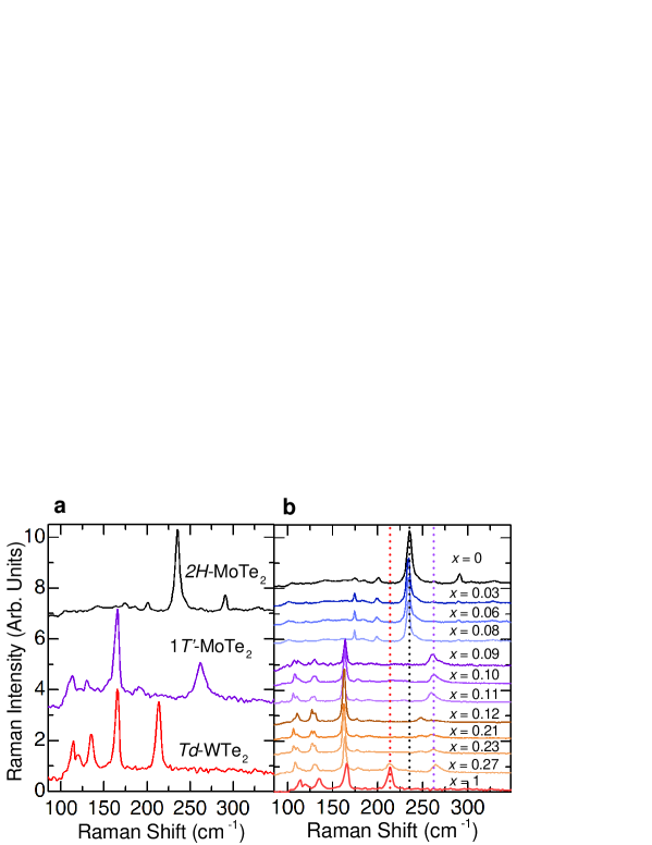
The structural phase transition as a function of doping is accompanied by changes in vibrational modes, as probed by Raman spectroscopy (see, Fig. 2). Figure 2a shows room-temperature Raman spectra obtained from the - and MoTe2 phases, and from WTe2. The structure displays two main Raman peaks at 174 cm-1 and 235 cm-1 corresponding to the and modes, respectively MoTe2_FETs ; Yamamoto . Reflecting its reduced symmetry, the phase displays several peaks at lower wave-numbers. For this structure the main peaks occur at 163 cm-1 and 260 cm-1 and have been indexed as the and modes MoTe2_MI_transition , respectively. WTe2 presents a spectrum having peaks occurring at 136 cm-1 and 165 cm-1 respectively, both of character Jiang , in addition to a peak at 210 cm-1 previously indexed as the mode. In Supplementary Fig. S6 we show Raman spectra for Mo0.88W0.12Te2 as the number of layers decrease, indicating that the -phase is stable down to the single-layer limit despite its high Mo content. Figure 2b shows Raman spectra for several stoichiometries of the Mo1-xWxTe2 series. Mo1-xWxTe2 crystallizes in the phase for concentrations up to . For concentrations beyond this value the spectra abruptly change, as indicated by the disappearance of the and of the peaks at 174 cm-1 and 235 cm-1 respectively, which are observed when . These data support the conclusions reached by the structural probes above, namely a phase transition around with no evidence for phase coexistence. Interestingly, As the W concentration increases beyond we see the emergence of peaks which, at the first glance, would seem to be related to the and the modes of the -phase MoTe2_MI_transition . However, single crystal ray diffraction shown in Fig. 1d and in Supplementary Fig. S3 clearly indicate that the Raman spectra in Fig. 2b must be associated with the orthorhombic phase, with certain peaks shifted with respect to those of WTe2 due to the high Mo content. An important observation is that Raman scattering yields nearly identical spectra for MoTe2 and for Mo1-xWxTe2, for reasons that will have to be clarified through theoretical calculations. We note that this similarity might lead to misidentification of the phase if Raman spectroscopy is the only method used to probe the crystal structure. In Supplementary Fig. S6, we show Raman scattering data as a function of the number of atomic layers for a crystal having , which is close to the critical concentration , indicating that it preserves its structure upon exfoliation despite its proximity to the phase-boundary. In Supplementary Fig. S7, we have include transport data, like the room temperature conductivity as a function of doping, which changes by orders of magnitude as one crosses the phase-boundary.
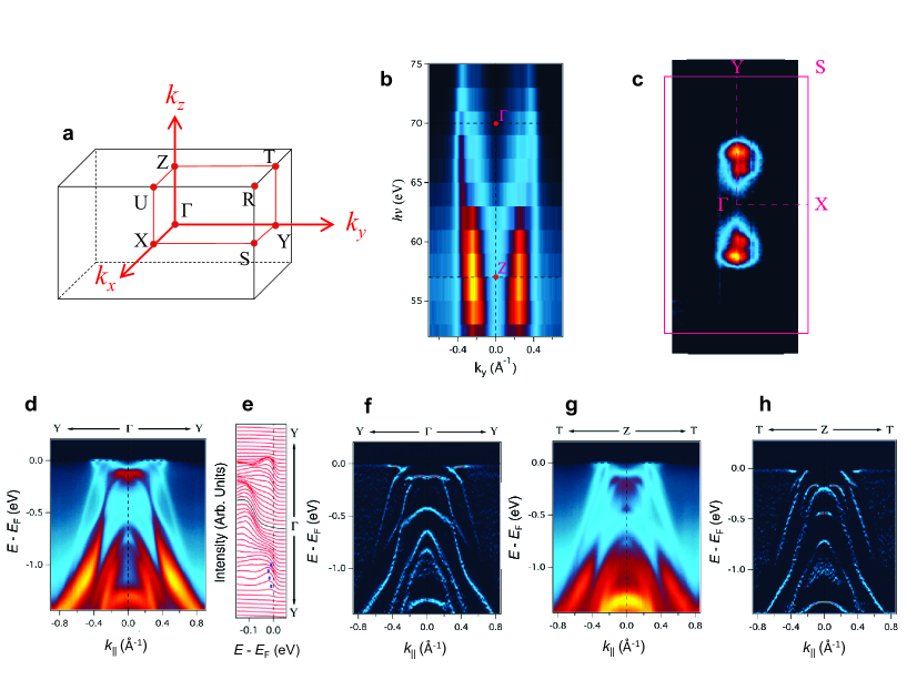
Next, we investigated the electronic phase-transition accompanying the structural phase transition. In particular, while the nature of the semiconducting phase is well understood, it is not known whether the phase in the W-doped material is a conventional, or a Weyl, semi-metallic system. Therefore, we investigated the electronic structure of heavily doped Mo1-xWxTe2 single crystals through angle-resolved photoemission spectroscopy (ARPES), as shown in Fig. 3. The core level spectrum, shown in the Supplementary Fig. S1, displays the characteristic peaks of W and Te elements, confirming that W is alloyed into the MoTe2 crystal. As seen in this figure, the W core levels have one set of doublets at 31.4 eV and 33.6 eV (right inset in Supplementary Fig. S1) respectively, in perfect agreement with the values found in the literature Arpes_book . Meanwhile the Te and doublets split into four peaks (left inset in Supplementary Fig. S1). This suggests that the Mo/W layer is sandwiched by the Te layers, making the Te layer the exposed surface. To investigate the electronic structure along the -direction of the three-dimensional Brillouin zone (BZ), which is depicted in Fig. 3a, we performed photon-energy-dependent ARPES measurements with energies ranging from 40 to 90 eV. Figure 3b shows the ARPES spectra at the Fermi level as a function of the momentum and photon energy from 55 to 75 eV. We extracted the positions of the and points from the dispersion as a function of , as shown. Figure 3c shows the Fermi surface of Mo0.73W0.27Te2 acquired at eV. The Fermi surface along the Y--Y direction shows two hole-pockets and two-electron pockets at either side of which would seem to touch. This geometry for the Fermi surface of Mo0.73W0.27Te2 (as well as its overall electronic band-structure) is remarkably similar to the one reported in Ref. Pletikosic, for WTe2 and therefore remarkably different from the one already reported ARPES_Huang for orthorhombic MoTe2. This difference is particularly striking given its considerably larger content of Mo relative to W. Notice that such a simple Fermi surface would be in broad agreement with our recent study QOs on the quantum oscillatory phenomena observed in -MoTe2.
ARPES band-maps along the high symmetry directions of a Mo0.73W0.27Te2 single crystal, as well as the corresponding plots of their second derivatives, are shown in Figs. 3d through 3h. Figs. 3d and 3f show band-maps, and corresponding second derivative, acquired with a photon energy of 70 eV along the Y--Y direction. Figs. 3g and 3h correspond to band maps and second derivatives collected along the T-Z-T direction with a photon energy of 57 eV corresponding to . The remarkable features near are the flat hole-like band crossing around Å-1, and an electron-like pocket in the vicinity of Å-1. The band connecting the hole- and the electron-like pockets is assigned to a surface state, which have already been claimed to be topologically nontrivial Hasan ; Belopolski . When compared to the calculations in Ref. Hasan, the conduction band minimum is observed to be very close to the Fermi level, which makes this surface state not as easily detectable as one would expect from the calculations. The surface state is more clearly exposed in Supplementary Fig. S8. Notice that the bands near at have higher binding energies than those at . As a result, the electron pocket and the surface state become more apparent in Figs. 3d and 3f.
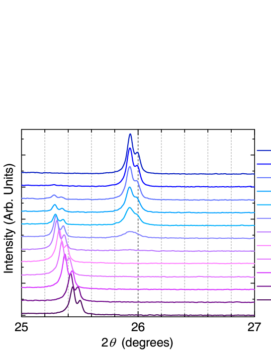
Having established the room temperature boundary between the and phases and explored the electronic structure of the latter phase, we now turn to the temperature axis of the phase-diagram. Figure 4 shows powder XRD patterns for a sample with , at different temperatures upon heating from room-temperature. Above ∘C, the peaks associated with the phase disappear and new peaks that can be ascribed to the phase appear. Similar studies for different compositions are shown in Supplementary Fig. S5. We find that the boundary is situated at C with a large, sample dependent uncertainty of the order of C previously attributed to variations in the Te stoichiometry MoTe2_MI_transition . The variation of as a function of remains within this uncertainty, therefore the boundary should be considered as doping independent. We do not see evidence for an extended region in temperature where both phases would coexistMoTe2_MI_transition . The MoTe2 phase continues to display a good degree of crystallinity at high s indicating that the structural transition is not driven by an increase in the number of Te vacancies or material degradation.
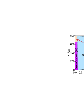
The proposed phase diagram, shown in Figure 5, depicts a sharp phase-boundary between the and the phases at , and the boundary between the and phases at C. In Supplementary Fig. S9 we compare ray powder diffraction data among samples crystallizing in the and in the phases and the role of the temperature. The important point is that, in contrast to the phase, and even for samples with a W concentration very close to the critical one, we could not detect a structural phase-transition as a function of in samples crystallizing in the phase. Given that the orthorhombic phase becomes the ground state of MoTe2 and the larger area occupied by it in the phase diagram, one is led to conclude that it is thermodynamically more stable than the latter phase. The most remarkable feature of the phase diagram is the very small concentration in W required to stabilize the orthorhombic semi-metallic phase, and not the coexistence of the and the phases as predicted by Ref. Alexander, , through a sharp boundary situated at . Such a sharp boundary points to a first-order phase-transition as a function of doping with the caveat that we could not detect phase coexistence.
It is quite remarkable that a semiconducting band gap as large as eVHeinz for MoTe2, can be entirely suppressed by substituting just % of Mo for W which stabilizes a semimetallic state, as clearly indicated by angle resolved photoemission experiments. Here, the situation bears a certain resemblance with the transition metal oxides such as the cuprates, whose charge- or Mott-gap is estimated to be eV, but where a small concentration of dopants, in the order of 5 %, is enough to stabilize a metallic state (albeit anomalous) and even superconductivity Patrick . This clearly indicates that both the structural and the concomitant electronic phases of MoTe2 are particularly susceptible to small perturbations. This suggests that it should be possible to reversibly induce structural-transitions through the application of strain Alexander or an electric field Reed , particularly in Mo1-xWxTe2 crystals with . This would make the Mo1-xWxTe2 series particularly appealing for the development of phase-change memory devicesAlexander ; reed1 ; Reed ; zhang or for a new generation of optoelectronic devices, whose metallic interconnects could be created or “erased” at will through the application of an electrical signal, instead of a chemical treatment. Finally, the fact that the Mo1-xWxTe2 series produce homogeneous alloys, is not only a major result of this study, but opens the unique possibility of exploring the evolution of their predicted topological/electronic properties Hasan , and of perhaps detecting topological phase-transitions in the bulk as well as in the surface state through the evolution of the Fermi surface. In effect, ARPES indicates that the Fermi surfaces of MoTe2 (Ref. ARPES_Huang, ) and of Mo1-xWxTe2 (this work) are remarkably different, a fact that can only be reconciled with an electronic/topological phase-transition as a function of W doping. In effect, since W doping tends to stabilize the -phase, it is reasonable to expect that one can stabilize it also in samples containing small amounts of W by quickly cooling the crystals to room temperature during the synthesis process. This would produce a phase-diagram not containing the region originally occupied by the phase. This set of orthorhombic samples would allow us to explore the evolution of the Fermi surface as a function of W doping to understand, for example, how the large hole-pocket seen by ARPES at the center of the Brillouin zone ARPES_Huang disappears to originate the hole-pockets seen by us at either side of zone center. Such electronic phase-transition should lead to either the suppression or the displacement of the Weyl-points already seen by ARPES, or to a concomitant topological phase-transition as a function of W doping.
Methods
Sample synthesis
For the synthesis of pure and MoTe2 as well as WTe2 Mo, 99.9999%, W, 99.9999 % and Te 99.9999 % were placed in a quartz ampoule in a ratio of 1:25 for growth in a Te flux. Subsequently, the material was heated up to 1050∘C and held there for 1 day. Then, the ampoule was slowly cooled down to 525∘C to yield either WTe2 or MoTe2 and then centrifuged. To produce the MoTe2 phase crystals were centrifuged at 900∘C. The “as harvested” single crystals were subsequently annealed for a few days at a temperature gradient to remove the excess Te. For Mo1-xWxTe2, single crystals were synthesized through a chemical vapor transport technique using iodine or TeCl4 as the transport agent. Samples were held at 750 ∘C with a 100 ∘C temperature gradient for 1 week, then subsequently cooled over 3 days to 400 ∘C and removed from the furnace. Each growth commonly yielded crystals of both structure types ( and ), except for those crystals very rich in Mo, i.e. . Stoichiometry was determined by energy dispersive ray spectroscopy (EDS) analysis through a field-emission scanning electron microscope (FEI Nova 400). A more precise stoichiometric determination was achieved using -ray photoelectron spectroscopy (XPS) either at the Shanghai Synchrotron Radiation Facility or at the Stanford Synchrotron Radiation Lightsource.
Scanning transmission electron microscopy
For scanning transmission electron microscopy imaging we used a JEOL 2200FS spherical aberration corrected tool operated under 200 kV. When using a 25.6 mrad convergence angle our probe size was 0.9 Å. Although 200 kV is most likely above the sample damage threshold, we used limited acquisition times and beam exposure to minimize the possible changes to the sample structure. Micro exfoliated few-layered samples were transferred onto TEM grids via a dry transfer method using polypropylene carbonate.
X-ray diffraction as a function of the temperature
Powder samples of Mo1-xWxTe2 were prepared by sonicating chemical vapor transport grown bulk crystals in hexane. The Mo1-xWxTe2 dispersion was then drop cast onto -axis sapphire substrates. This preparation led to highly textured powders, with the -axis of the sample roughly aligned with the substrate surface normal. Heating X-ray diffraction measurements were carried out in a PANalytical X’Pert 2 diffractometer with an Anton-Paar domed hot stage that was purged with ultra pure nitrogen. X-rays were generated from a copper target, with the Cu Kβ radiation removed by using a nickel filter. Several samples were also prepared via exfoliation of bulk crystals onto sapphire substrates. The phase-transition temperature was found to be independent on the method used.
Scanning tunneling microscopy
Scanning tunneling microscopy (STM) measurements were performed with a home built variable temperature, ultra high vacuum STM system at K. Single crystalline Mo1-xWxTe2 was mounted onto metallic sample holders using a vacuum safe silver paste. Samples were transferred into the STM chamber and cleaved in-situ to expose a clean surface on which measurements were performed. The Pt-Ir STM tip was cleaned and calibrated against a gold (111) single crystal prior to the measurements.
Angle resolved photoemission spectroscopy
ARPES measurements were performed at the Dreamline beamline of the Shanghai Synchrotron Radiation Facility with a Scienta D80 analyzer. The energy and angular resolutions were set to 15 meV and , respectively. The ARPES data were collected using horizontally-polarized light with a vertical analyzer slit. The samples were cleaved in situ and measured at K in a vacuum better than Torr. The cleaved surfaces are observed to be flat at a scale m while the beam spot size of the incident light is m2, therefore the electronic structure probed by us is from a single domain.
References
- (1) Revolins, E. & Beerntse D. J. Electrical properties of - and -MoTe2 as affected by stoichiometry and preparation temperature. J. Phys. Chem. Solids 27, 523-526 (1966).
- (2) Vellinga, M. B., de Jonge, R., & Haas, C. Semiconductor to metal transition in MoTe2 J. Solid State Chem. 2, 299-302 (1970).
- (3) Voiry, D. Mohite, A. & Chhowalla, M. Phase engineering of transition metal dichalcogenides. Chem. Soc. Rev. 44, 2702-2712 (2015).
- (4) Keum, D. H., et al. Bandgap opening in few-layered monoclinic MoTe2. Nature Phys. 11, 482-486 (2015).
- (5) Ruppert, C. Aslan, O. B. & Heinz, T. F. Optical Properties and Band Gap of Single- and Few-Layer MoTe2 Crystals. Nano Lett. 14, 6231–6236 (2014).
- (6) Soluyanov, A. A. et al. A New Type of Weyl Semimetals. Nature 527, 495-498 (2015).
- (7) Sun, Y. Wu, S.C. Ali, M. N. Felser, C. & Yan, B. Prediction of the Weyl semimetal in the orthorhombic MoTe2. Phys. Rev. B 92, 161107 (2015).
- (8) Wang, Z. et al. MoTe2: A type-II Weyl Topological Metal. Phys. Rev. Lett. 117, 056805 (2016).
- (9) Qian, X. F. Liu, J. W. Fu, L. & Li, J. Quantum spin Hall effect in two-dimensional transition metal dichalcogenides. Science 346, 1344 (2014).
- (10) Duerloo, K. A. N. Li, Y. Reed, E. J. Structural phase transitions in two-dimensional Mo- and W-dichalcogenide monolayers. Nat. Commun. 5, 4214 (2014).
- (11) Duerloo, K. A. N. & Reed, E. J. Structural Phase Transitions by Design in Monolayer Alloys. ACS Nano 10, 289-297 (2016).
- (12) Kappera, R. et al. Phase-engineered low-resistance contacts for ultrathin MoS2 transistors. Nature Mater. 13, 1128-1134 (2014).
- (13) Cho, S. et al. Phase patterning for ohmic homojunction contact in MoTe2. Science 349, 625-628 (2015).
- (14) Li, Y., Duerloo, K.-A. N., Wauson, K. & Reed, E. J. Structural semiconductor-to-semimetal phase transition in two-dimensional materials induced by electrostatic gating. Nat. Commun. 7, 10671 (2016).
- (15) Zhang, C. et al. Charge Mediated Reversible Metal−Insulator Transition in Monolayer MoTe2 and WxMo1−xTe2 Alloy. ACS Nano 10, 7370−7375 (2016).
- (16) Pletikosić, I., Ali, M. N., Fedorov, A. V. Cava, R. J. & Valla, T. Electronic Structure Basis for the Extraordinary Magnetoresistance in WTe2, Phys. Rev. Lett. 113, 216601 (2014).
- (17) Lezama, I. G. Ubaldini, A. Longobardi, M. Giannini, E. Renner, C. Kuzmenko, A. B. Morpurgo, A. F. Surface transport and band gap structure of exfoliated -MoTe2 crystals. 2D Materials 1, 021002 (2014).
- (18) Lezama, I. G. Arora, A. Ubaldini, A. Barreteau, C. Giannini, E. Potemski, M. Morpurgo, A. F. Indirect-to-Direct Band Gap Crossover in Few-Layer MoTe2. Nano Lett. 15, 2336-2342 (2015).
- (19) Pradhan, N. R. et al. Field-Effect Transistors Based on Few-Layered alpha-MoTe2. ACS Nano 8, 5911-5920 (2014).
- (20) Lin, Y. F. et al. Ambipolar MoTe2 Transistors and Their Applications in Logic Circuits. Adv. Mater. 26, 3263–3269 (2014).
- (21) Mak, K. F. & Shan, J. Photonics and optoelectronics of 2D semiconductor transition metal dichalcogenides. Nature Photon. 10, 216-226 (2016).
- (22) Park, J. C. et al. Phase-Engineered Synthesis of Centimeter-Scale - and -Molybdenum Ditelluride Thin Films. ACS Nano 9, 6548-6554 (2015).
- (23) Zhang, W. Chiu, M. H. Chen, C. H. Chen, W. Li, L. J. & Wee, A. T. S. Role of Metal Contacts in High-Performance Phototransistors Based on WSe2 Monolayers. ACS Nano 8, 8653-8661 (2014).
- (24) Alexander, K.-, Duerloo N. & Reed, E. J. Structural Phase Transitions by Design in Monolayer Alloys. ACS Nano 10, 289-297 (2016).
- (25) Zhang, C., KC, S., Nie, Y., Liang, C., Vandenberghe, W. G., Longo, R. C., Zheng, Y., Kong, F., Hong, S., Wallace, R. M. & Cho, K. Charge Mediated Reversible Metal-Insulator Transition in Monolayer MoTe2 and WxMo1−xTe2 Alloy, ACS Nano 10, 7370-7375 (2016).
- (26) Weng, H. M. Fang, C. Fang, Z. Bernevig, B. A. & Dai, X. Weyl Semimetal Phase in Noncentrosymmetric Transition-Metal Monophosphides. Phys. Rev. X 5, 011029 (2015)
- (27) Xu, S. Y. et al. Discovery of a Weyl fermion semimetal and topological Fermi arcs. Science 349, 613-617 (2015).
- (28) Chang, T. R. et al. Prediction of an arc-tunable Weyl Fermion metallic state in MoxW1-xTe2, Nat. Commun. 7, 10639 (2016).
- (29) Huang, L. et al. Spectroscopic evidence for a type II Weyl semimetallic state in MoTe2. Nat. Mater. doi:10.1038/nmat4685 (2016).
- (30) Champion, J. A. Some propertities of (Mo,W)(Se,Te)2. Brit. J. Appl. Phys. 16, 1035 (1965).
- (31) Yamamoto, M. et al. Strong Enhancement of Raman Scattering from a Bulk-Inactive Vibrational Mode in Few-Layer MoTe2. ACS Nano 8, 3895-3903 (2014).
- (32) Jiang, Y. C. et al. Raman fingerprint for semimetal WTe2 evolving from bulk to monolayer. Sci. Rep. 6, 19624 (2016).
- (33) Chastain, J., & King, R. C. Eds. Handbook of X-ray photoelectron spectroscopy: a reference book of standard spectra for identification and interpretation of XPS data. Eden Prairie, MN: Physical Electronics, 1995.
- (34) Pletikosic, I. Ali, M. N., Fedorov, A. V., Cava, R. J., & Valla, T. Electronic Structure Basis for the Extraordinary Magnetoresistance in WTe2. Phys. Rev. Lett. 113, 216601 (2014).
- (35) Belopolski, I. et al. Fermi arc electronic structure and Chern numbers in the type-II Weyl semimetal candidate MoxW1−xTe2. Phys. Rev. B 94, 085127 (2016).
- (36) Rhodes, D. et al. Impurity dependent superconductivity, Berry phase and bulk Fermi surface of the Weyl type-II semimetal candidate MoTe2. arXiv:1605.09065 (2016).
- (37) Lee, P. A., Nagaosa, N. & Wen, X.-G. Doping a Mott Insulator: Physics of High Temperature Superconductivity. Rev. Mod. Phys. 78, 17-85 (2006).
Acknowledgements.
†These authors contributed equally to this work. The subsequent order of authorship do not reflect the relative importance among the contributions from the different authors and groups. Their contributions to this work should be considered of equal relevance. L. B. is supported by the U.S. Army Research Office MURI Grant W911NF-11-1-0362. This work was supported in part by the Molecular and Electronic Nanostructures theme of the Beckman Institute at UIUC. Electron microscopy work was performed at the Frederick Seitz Materials Research Laboratory Central Research Facilities, University of Illinois. Single-crystal X-ray diffraction was performed in the Shared Materials Characterization Laboratory at Columbia University. AML acknowledges support by the U.S. Department of Energy, Basic Energy Sciences, Materials Sciences and Engineering Division. The work of R.M.O., J.I.D., W.J., and Y.L. was financially supported by the U.S. Department of Energy under Contract No. DE-FG 02-04-ER-46157. F.E. gratefully acknowledges Grant LPDS 2013-13 from the German National Academy of Sciences Leopoldina. This work was also supported by the DOE-BES, Materials Sciences and Engineering Division, under Contract DE-AC02-76SF00515 and by the W. M. Keck Foundation and the Gordon and Betty Moore Foundation’s EPiQS Initiative through Grant No. GBMF4545. D.C., N.F., A.A. and J.H. acknowledge support from AFOSR grant FA9550-14-1-0268. R.L. and S.C.W. were supported by the National Natural Science Foundation of China (No. 11274381). J.Z.M., T.Q., and H.D. were supported by the Ministry of Science and Technology of China (No. 2015CB921300, No. 2013CB921700), the National Natural Science Foundation of China (No. 11474340, No. 11234014), and the Chinese Academy of Sciences (No. XDB07000000). STM work is supported by AFOSR (FA9550-11-1-0010, DE) and NSF (DMR-1610110, ANP). This research used resources of (XPS at) the Center for Functional Nanomaterials, which is a U.S. DOE Office of Science Facility, at Brookhaven National Laboratory under Contract No. DE-SC0012704. The NHMFL is supported by NSF through NSF-DMR-1157490 and the State of Florida.Author contributions
D.R. synthesized and characterized the single crystals through electron dispersive spectroscopy, Raman scattering and transport measurements. Y.-c.C., W.Z., and Q.R.Z. were directly involved in the synthesis and in the preliminary characterization of the crystals. D.C., T.K., A.M., M.C., M.D., N.F., A.A., and J.H. motivated the project, performed Raman, photoluminescense and device characterization. B.E.J. and P.Y.H. performed atomic resolution STEM transmission electron microscopy. W.J., J.Z.M., R.L., T.S., S.C.W., T.Q., H.D., J.I.D., and R.M.O. performed angle-resolved photoemission spectroscopy measurements. Y.L., X.T., T.S., J.I.D., and R.M.O. performed x-ray photoemission spectroscopy measurements. D.E. and A.N.P. performed scanning tunneling spectroscopy measurements. C.N., E.M., F.E., and A.M.L. performed powder X-ray and electron diffraction measurements as function of the temperature. D.W.P. Performed single crystal ray diffraction. D. R., J. H. and L. B. wrote the manuscript with the input of all co-authors.
Additional information
Supplementary information is available in the online version of the paper. Reprints and permissions information is available online at www.nature.com/reprints. Correspondence and requests for materials should be addressed to L.B.
Competing financial interests
The authors declare no competing financial interests.