Probing the semiconductor to semimetal transition in InAs/GaSb double quantum wells by magneto-infrared spectroscopy
Abstract
We perform a magneto-infrared spectroscopy study of the semiconductor to semimetal transition of InAs/GaSb double quantum wells from the normal to the inverted state. We show that owing to the low carrier density of our samples (approaching the intrinsic limit), the magneto-absorption spectra evolve from a single cyclotron resonance peak in the normal state to multiple absorption peaks in the inverted state with distinct magnetic field dependence. Using an eight-band Pidgeon-Brown model, we explain all the major absorption peaks observed in our experiment. We demonstrate that the semiconductor to semimetal transition can be realized by manipulating the quantum confinement, the strain, and the magnetic field. Our work paves the way for band engineering of optimal InAs/GaSb structures for realizing novel topological states as well as for device applications in the terahertz regime.
pacs:
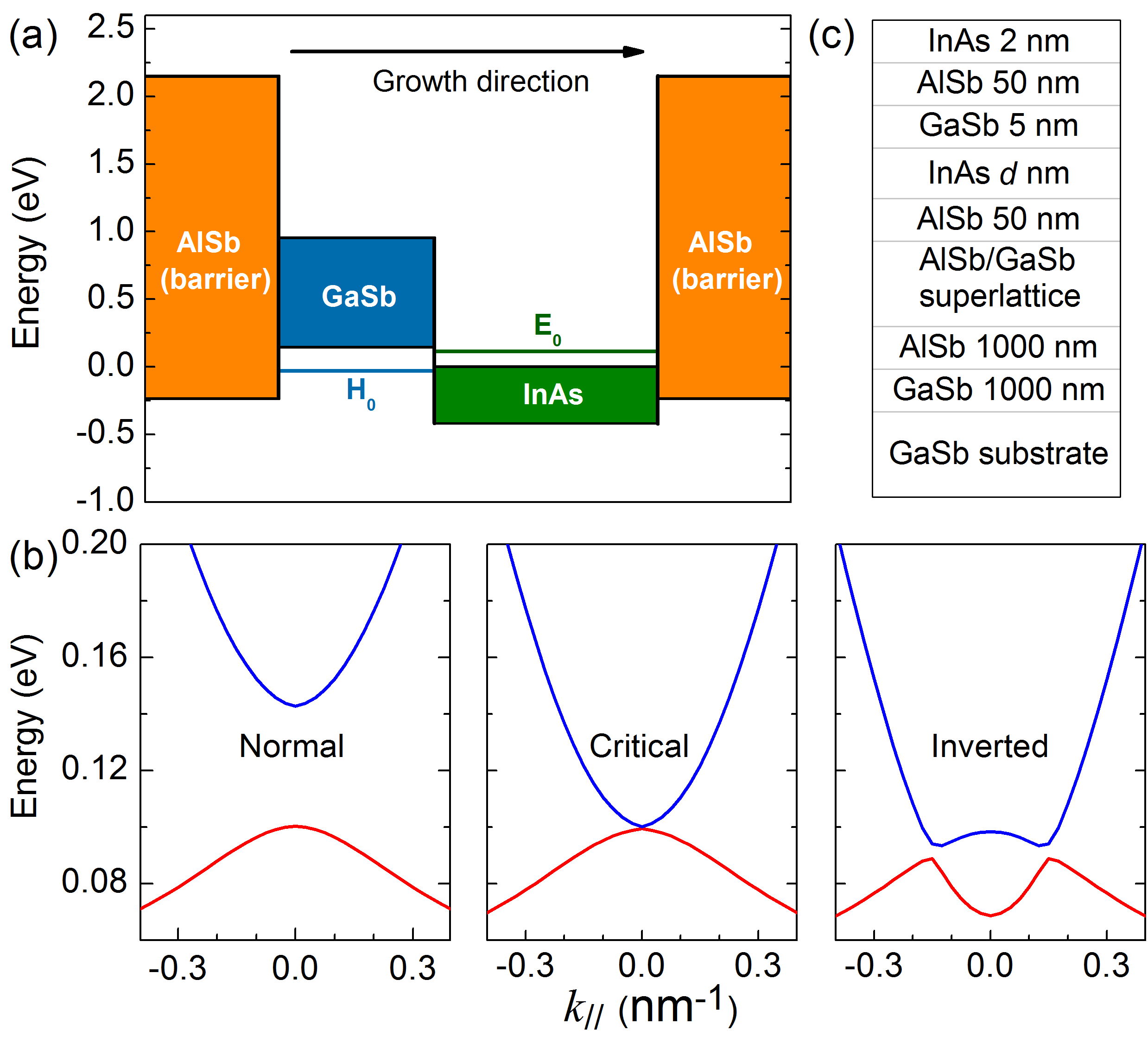
76.40.+b, 71.70.Di, 78.20.Ls, 73.21.FgBroken-gap InAs/GaSb double quantum wells (DQWs) have long been important in studying intriguing phenomena, ranging from excitonic resonances Kono_PRB1 ; Tung_PRB1 , electron-hole hybridization Nicholas_SST1 ; Yang_PRL ; Marlow_PRL ; Nicholas_PRB1 , the quantum spin Hall (QSH) effect Liu_PRL ; Du_PRL2 ; Ihn_PRB , helical Luttinger liquids Du_PRL3 , to the exciton insulator Du_arXiv . The novel properties of the InAs/GaSb system stem from its peculiar band-edge alignment, in which the bottom of the InAs conduction band lies below the top of the GaSb valence band (Fig. 1(a)), resulting in the separation of electrons and holes into the two QWs. By changing the width of each QW, one can manipulate the electron and hole energy levels using the quantum confinement effect. Specifically, when the lowest electron level in InAs lies above the highest hole level in GaSb, the system is in the normal state (). When the opposite alignment is achieved, the system is said to be in the inverted state. The transition from normal to inverted states occurs at the critical QW widths at which (Fig. 1(b)). Recently, the QSH effect has been theoretically predicted Liu_PRL and experimentally confirmed Du_PRL2 in the inverted regime, while an exotic exciton insulator state Du_arXiv and a giant supercurrent state Shi_JAP have been found in the vicinity of the critical state. Therefore, precise control of band alignment of InAs/GaSb DQWs from the normal to the inverted state is crucial for future fundamental studies. In particular, a thorough understanding of strain effects may lead to a robust QSH insulator state suited for realizing Majorana fermions Du_new .
From technological perspective, InAs/GaSb-based materials are promising candidates for third-generation infrared (IR) detectors Martyniuk , high-power light emitting diodes Prineas , and tunnel field-effect transistors Hudait , owing to their band engineering flexibility and the resulting low Auger recombination rates Ehrenreich . Practical applications of the material require a complete understanding of the electronic band structure, with respect to external parameters such as strain and doping. Previous combined experimental and theoretical studies Nicholas_SST1 ; Yang_PRL ; Marlow_PRL ; Nicholas_PRB1 largely focused on the heavily inverted regime using reduced models. Quantitative investigations of the transition from the normal to the inverted state have not yet been performed.
In this Letter, we study the evolution of the electronic band structure of InAs/GaSb DQWs across the semiconductor to semimetal transition using magneto-IR spectroscopy. The observed magneto-optical modes can be explained using an eight-band model, and semi-quantitive agreement is achieved. We show that in addition to the commonly used electrostatic gate, the normal to the inverted state transition can be manipulated in a much larger parameter space via tuning the relative thickness of the QWs, the strain, and the magnetic field.
The InAs/GaSb DQW samples studied in this work were grown by molecular beam epitaxy (MBE) on GaSb (001) substrates. A schematic of the epi-structure is shown in Fig. 1(c), where the InAs/GaSb DQW structure is sandwiched between two AlSb barrier layers. To study the normal to inverted transition, we fabricated a series of five InAs/GaSb DQW samples. We fixed the width of the GaSb QW at 5 nm, while varying the InAs QW width from to , 11, 13, and 15 nm. Based on our self-consistent eight-band calculation (to be elaborated later), the nm sample is in the normal state, the nm sample is close to the critical state and the , 13, and 15 nm samples are in the inverted state. Magneto-transport measurements determined the carrier densities to be as low as cm-2 Shi_JAP , several times lower than that reported in previous studies Kono_PRB1 ; Tung_PRB1 ; Nicholas_SST1 ; Marlow_PRL ; Nicholas_PRB1 . Therefore, our samples are close to the intrinsic limit, particularly suited for magneto-optical spectroscopy studies.
Magneto-IR spectroscopy measurements were performed in the Faraday configuration at liquid helium temperature (4.2 K) using a Bruker 80v Fourier-transform IR spectrometer. The (unpolarized) IR radiation from a mercury lamp was delivered to the sample located at the center of a 17.5 T superconducting magnet via evacuated light-pipes, and the intensity of the transmitted light was detected by a composite Si bolometer mounted beneath the sample. Normalized magneto-absorption spectra were then obtained by taking the ratio of , where is the transmission spectrum measured at a constant magnetic field . In this scenario, the intra-band (cyclotron resonance, CR) and inter-band Landau level (LL) transitions are expected to manifest themselves as a series of absorption peaks.
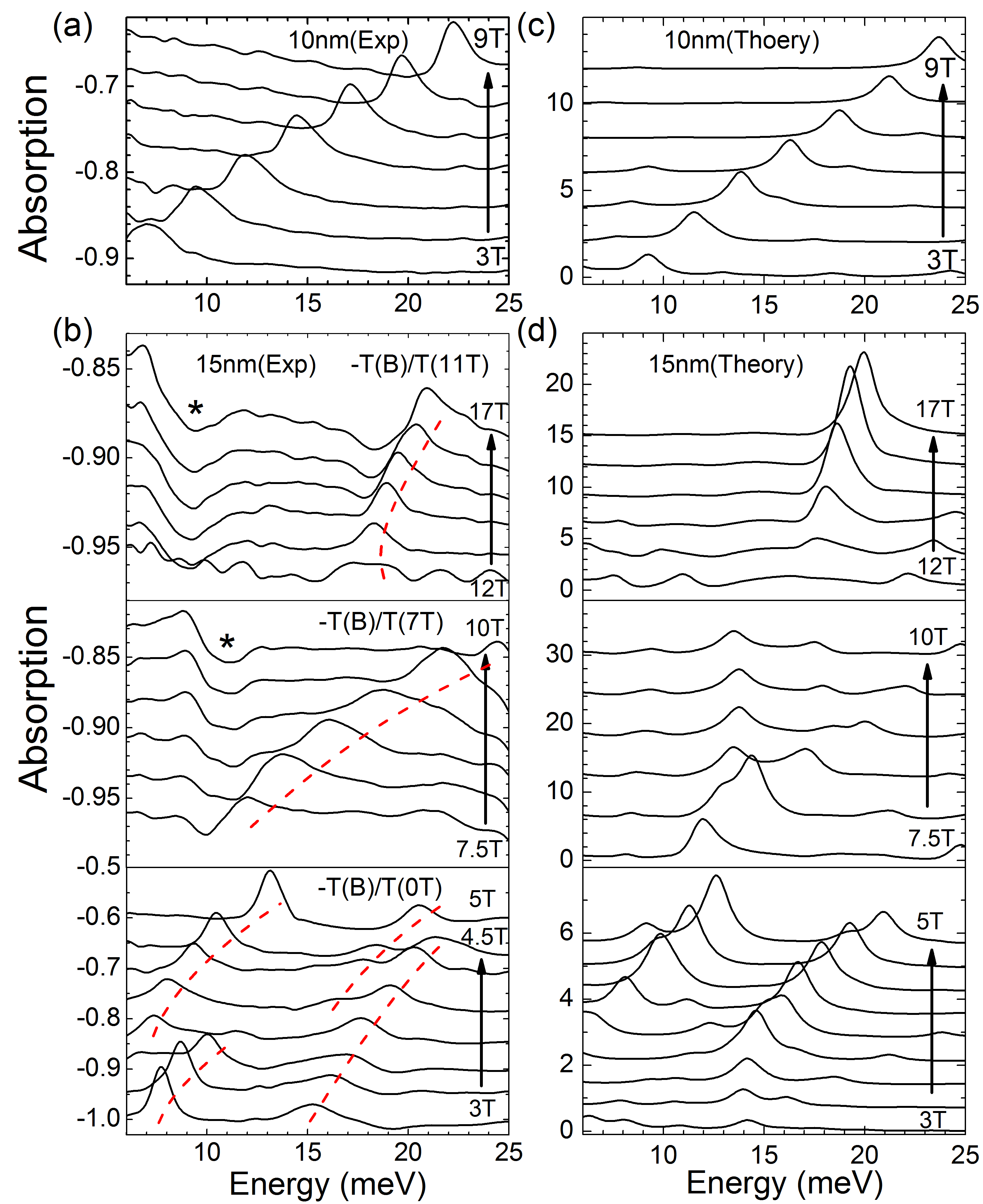
Figure 2(a) shows normalized magneto-absorption spectra, , for the nm DQW sample at selected magnetic fields. Here, the spectra exhibit a single symmetric line, indicative of a single absorption peak within the energy range of our measurements. The spectral lineshape becomes asymmetric and substantially broadened in the nm sample, as shown in Fig. S1 in the Supplemental Material SM . As the InAs QW width increases further to nm (Fig. S2) and nm (Fig. 2(b)), the InAs/GaSb DQWs enters a heavily inverted regime and multiple absorption peaks appear. Experimentally, one can identify four peaks for the case of nm in Fig. 2(b) in the low-field region, T. The two lower energy peaks are CR-like, , while the higher energy ones can be attributed to inter-band LL transitions. Interestingly, the CR-like peaks deviate from their linear-in- dependence at higher magnetic field (better seen in Fig. 4(d)), suggestive of LL crossing/anti-crossing. This behavior is consistent with that theoretically predicted in Ref. Chao_PRB2 . In the middle and upper panels of Fig. 2(b), one can find another two absorption peaks with distinct -dependence. In particular, the high-field peak exhibits very weak -dependence, similar to that reported for InAs/GaSb superlattices in Ref. Nicholas_SST1 . The observation of a total of six absorption peaks in the nm DQW sample (Fig. 4(d)) can be attributed to its low carrier density (approaching the intrinsic limit). However, the literature lacks a quantitative model that can interpret all these peaks.
To explain how band inversion changes the LL transitions in InAs/GaSb DQWs, we employ an eight-band Pidgeon-Brown (PB) model Pidgeon_PR that includes the interaction between the conduction and valence bands, the Zeeman energy, and the effect of spin-orbit coupling. The PB model is based on an eight-band method, described in the literature Chao_PRB1 ; Chao_JPCM1 ; Chao_PRB2 ; Kai_PRB1 ; Kai_APL ; Zhou_PRB , which has been successfully used for achieving semi-quantitative understanding of the electronic and magneto-optical properties of narrow-gap semiconductors Stanton_PRB1 ; Stanton_PRB2 ; Stanton_JAP ; Buhmann_PRB1 . We paid special attention to two important effects: (1) the effect of strain due to the lattice mismatch among different QW layers, and (2) the effect of charge transfer through the InAs/GaSb interface. We assume that the system is under pseudomorphic strain and all the QW in-plane lattice constants are pinned to the in-plane lattice constant of the GaSb substrate. The strain gives rise to an energy shift of a few tens of meV and drives the system towards a more inverted band alignment. This effect is significant for all the DQW samples studied. The charge transfer effect, on the other hand, is appreciable only in the inverted state Esaki when the valence band of GaSb overlaps with the conduction band of InAs. This overlap leads to charge redistribution across the InAs/GaSb interface, which consequently modifies the potential profile in DQWs. The charge transfer effect counters, or even overpowers, the strain effect in heavily inverted InAs/GaSb samples. It can be accommodated by solving the equations iteratively until the potential profile reaches convergence. Further detailed information (including an improved self-consistent algorithm) can be found in the Supplemental Material SM .
In the presence of a magnetic field, the total effective mass Hamiltonian of InAs/GaSb DQWs can be written as
| (1) |
where , , , and are the Landau, Zeeman, strain, and confinement Hamiltonian, respectively. Following the PB formalism, one can then solve the Schrödinger equation with a convenient set of envelope functions in the axial approximation,
| (2) |
where the integer is the PB manifold index and , and the integer labels the eigenvectors/eigenenergies belonging to the same index . We note that the Landau Hamiltonian in Eq. (1) is -dependent, whereas , , and are independent of . The explicit expressions of these terms are given in Refs. Stanton_PRB1 ; Stanton_PRB2 . Next, the matrix eigenvalue equations of Eq. (2) can be solved separately for each allowed value of and the eigenenergy is obtained as a function of magnetic field.
The calculated energy levels and Fermi energy are plotted as a function of magnetic field in Fig. 3 and Fig. S3 for all the DQW samples studied. The PB manifold is color coded based on the index , and for simplicity we only show the lowest levels, i.e., when , 0, 1, and 2. As one can clearly see in Fig. 3, the band structure of InAs/GaSb DQWs exhibits a transition from the normal to the inverted state with increasing InAs QW width . In the normal state (Fig. 3(a)), the electron (hole) levels reside in the conduction (valence) band and the energy of each level shows a monotonic -dependence without any crossing. In contrast, when the band is inverted (Figs. 3(b-d)), hole-like levels may exist at the bottom of the conduction band while electron-like levels appear at the top of the valence band. These levels inevitably cross or anti-cross each other at sufficiently high magnetic field, leading to multiple magneto-absorption peaks. The magnitude of the crossing/anti-crossing magnetic field therefore characterizes the degree of band inversion. One can see from Fig. 3 that the nm DQW sample is only slightly inverted, whereas the nm and 15 nm samples are heavily inverted. In addition, we note that even for a heavily inverted band structure, the electron-like levels in the valence band can be lifted above all the hole-like levels, at sufficiently high magnetic fields, driving the system to the normal state Kono_PRB1 ; Comment2_theory ; Comment2_Nicholas ; Comment2_proceeding . We will return to this magnetic field driven semimetal to semiconductor transition in the context of Fig. 5.
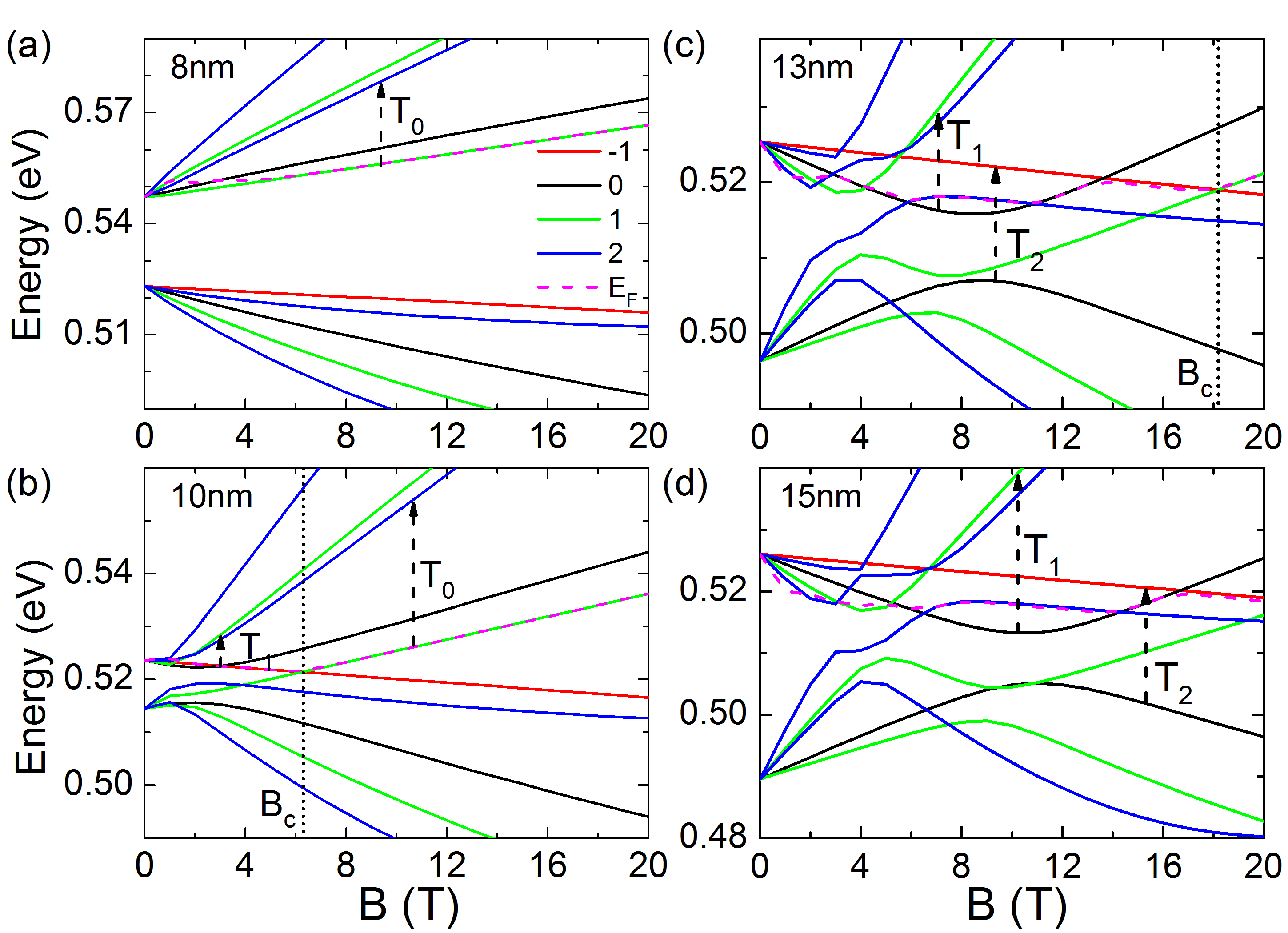
In order to calculate the magneto-optical absorption spectra, we first determine using a standard routine described in Ref. Stanton_PRB1 assuming an electron density of cm-2. Second, we compute the magneto-absorption coefficient using the wavefunctions obtained from the PB model and Fermi’s golden rule Stanton_PRB1 ; Stanton_PRB2 . The full width at half maximum (FWHM) is taken to be 0.8 meV in our calculation, estimated from the experimental data. The deduced selection rule reads , where () denotes electron (hole) like transitions. Figures 2(c,d) show the calculated magneto-absorption spectra for the slightly inverted ( nm) and heavily inverted ( nm) DQW samples, in comparison with the experimental data in Figs. 2(a,b). The same normalization method is applied to both the experimental and theoretical results. Here, as one can see, the calculated spectra capture all the absorption peaks observed in the experiment, although the relative strength between these peaks does not exhibit a perfect match. Better understanding of the data can be attained using the manifold-resolved magneto-absorption spectra, some examples of which are shown in Fig. S4. Manifold-resolved calculations help assign a specific transition to each absorption peak observed in our experiment. For example, the CR peak observed in the sample can be attributed to the transition from a level to a level (), as illustrated in Fig. 3(a). The manifold-resolved results are summarized in Fig. 4, where intra-band (inter-band) transitions are color coded in red (blue). Semi-quantitative agreement between the theory and experiment is reached note1 .
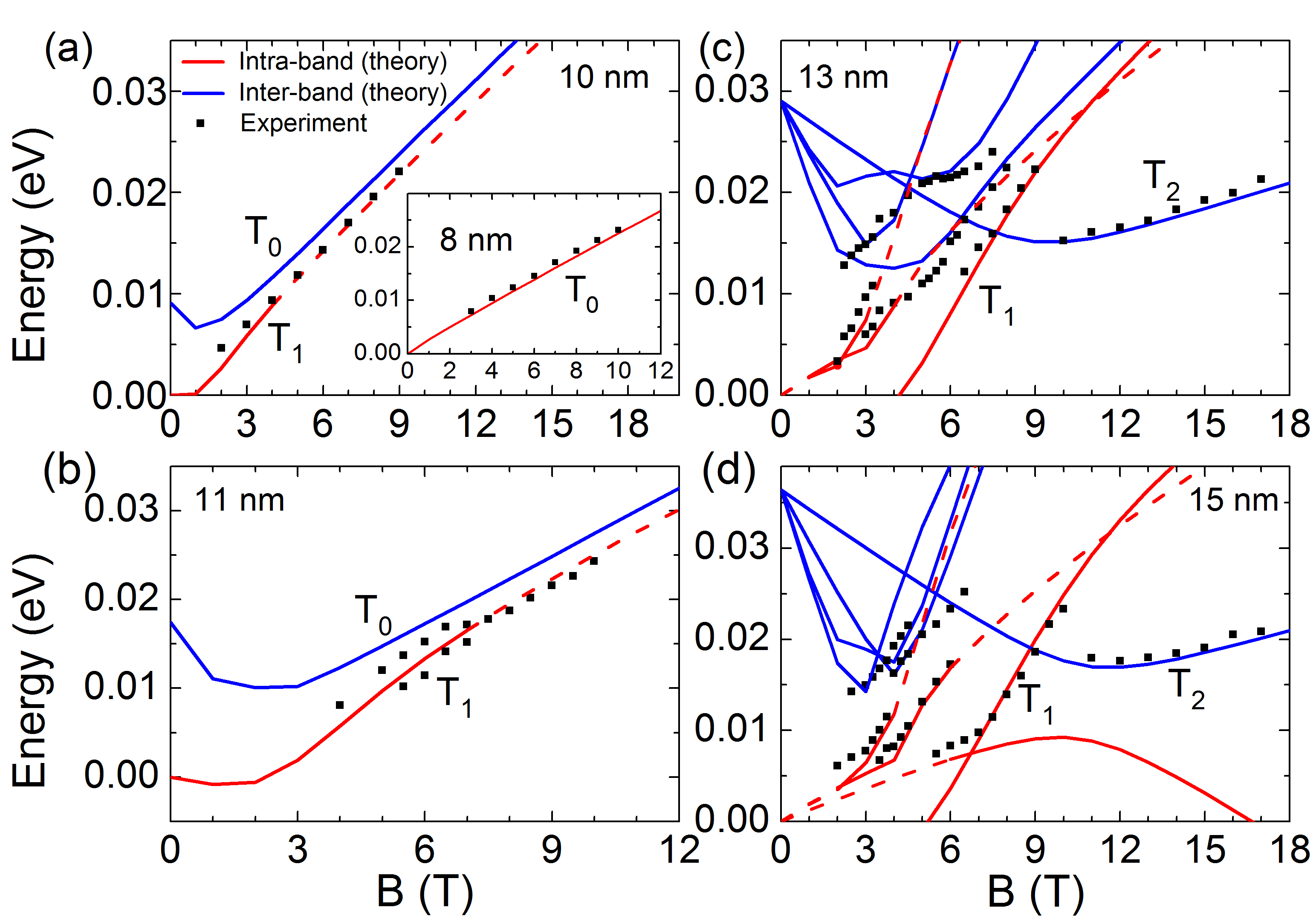
It is important to note that our eight-band PB calculation is based on the band parameters reported in Ref. Vurgaftman2001 with only two adjustable variables. One is the carrier density (or Fermi energy), which is set to be cm-2 for all the samples. As our DQWs are close to the intrinsic limit, the Fermi energy is expected to be quickly pinned to the lowest electron level with increasing magnetic field. The fact that only one absorption peak () is observed in the normal state ( nm) and slightly inverted ( nm) samples suggests an upper bound for the electron density, cm-2. The slight broadening of the CR linewidth in the nm sample at T is indicative of the presence of the transition (Fig. 3(b)), which sets the lower bound for . Therefore, one can conclude that cm-2 is a good approximation. The other variable used in our calculation is the effective mass of electrons in InAs QW, which is determined experimentally as by fitting to the CR () peak in the normal state ( nm) sample. Here, is the bare electron mass. In the inverted state, the contribution of to the band structure is coupled to that of the charge transfer effect discussed above. Therefore, can only be extracted accurately from the normal state data.
In addition to the transition, it is intriguing to investigate the (intra-band, ) and (inter-band, ) transitions denoted in Figs. 3 and 4. We note that in the normal state, is indiscernible from the transition. It starts to depart from when the band is slightly inverted (Figs. 4(a,b)), therefore it is responsible for the asymmetric lineshape observed in the nm sample (Fig. S1). As the band is further inverted, becomes a well-developed peak (Figs. 4(c,d)), but only occurs when the magnetic field lifts the level (green) above the level (black), as shown in Figs. 3(c,d). Therefore, can be used as an effective band-inversion indicator, and practically one can perform a linear-in- fit to its energy at relatively high magnetic field, with the fitting intercept for the normal state, for the inverted state, and more negative value being more inverted. On the other hand, the transition only occurs in the inverted state and in the high-field region. It exhibits very weak -dependence, distinct from all the other absorption peaks we have observed. We attribute this peak to a hole-like inter-band transition, , due to the uplift of the heavy hole level to the conduction band (i.e., band inversion). This observation is consistent with that reported in Ref. Nicholas_SST1 .
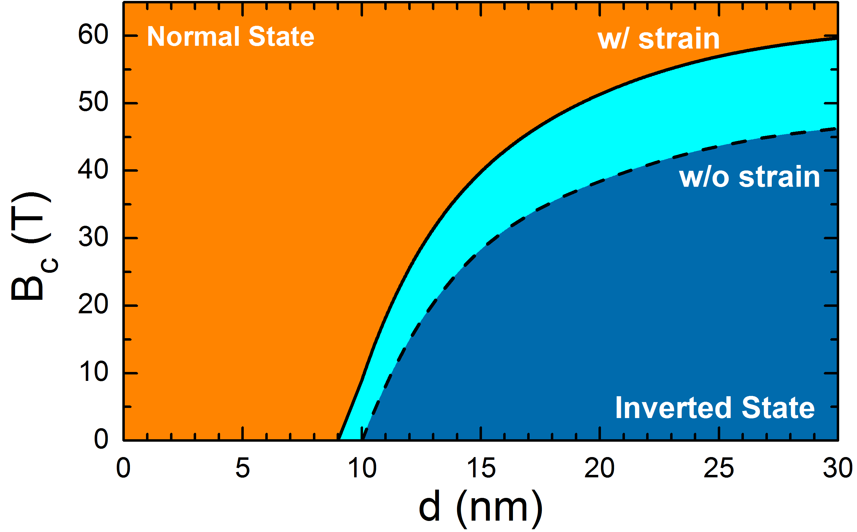
Lastly, we return to the magnetic field driven semimetal to semiconductor transition from the inverted to the normal state. As mentioned above, the heavy hole level (), inverted to the conduction band, would eventually cross below the lowest electron level () with increasing magnetic field, driving the system back to the normal state. A critical field can be defined at this crossing point (Figs. 3(b,c)), and the corresponding transition diagram is plotted in Fig. 5. The importance of the strain effect can also be seen in Fig. 5, as it significantly shifts the boundary between the inverted state and the magnetic field driven normal state. Practically, the strain effect can be engineered by choosing the appropriate substrate (typically, GaSb for pseudomorphic growth, GaAs for metamorphic growth) and the epi-structure Du_new .
In conclusion, we have studied the LL structure of a series of InAs/GaSb DQWs from the normal to the inverted state using magneto-IR spectroscopy. We find that close to the intrinsic limit, the band inversion significantly modifies the magneto-absorption of the system, giving rise to multiple absorption peaks with distinct non-linear -dependence. All the major absorption peaks observed in our experiment can successfully be explained using an eight-band PB model, with semi-quantitative agreement surpassing the previous two-band Nicholas_PRB1 and six-band Nicholas_SST1 models. The application of our model to InAs/GaSb multilayers and superlattices is currently in progress.
We thank Danhong Huang for helpful discussion. This work was primarily supported by the DOE (Grant No. DE-FG02-07ER46451). S.T., G.D.S., and C.J.S. acknowledge support from the NSF (Grant No. DMR-1311849) and the AFOSR (Grant No. FA9550-14-1-0376). Q.Z. and J.K. acknowledge support from the NSF (Grant No. DMR-1310138). The work at SNL is supported by the DOE Office of Basic Energy Sciences, Division of Materials Science and Engineering, and by Sandia LDRD. Sandia National Laboratories is a multi-program laboratory managed and operated by Sandia Corporation, a wholly owned subsidiary of Lockheed Martin Corporation, for the United States Department of Energy’s National Nuclear Security Administration under contract DE-AC04-94AL85000. The magneto-IR measurements were performed at the NHMFL, which is supported by the NSF Cooperative Agreement No. DMR-1157490 and the State of Florida.
References
- (1) J. Kono et al., Phys. Rev. B 50, 12242(R) (1994); ibid 55, 1617 (1997); J.-P. Cheng et al., Phys. Rev. Lett. 74, 450 (1995).
- (2) L.-C. Tung, P. A. Folkes, G. Gumbs, W. Xu, and Y.-J. Wang, Phys. Rev. B 82, 115305 (2010).
- (3) G. M. Sundaram, R. J. Warburton, R. J. Nicholas, G. M. Summers, N. J. Mason, and P. J. Walker, Semicond. Sci. Technol. 7, 985 (1992).
- (4) M. J. Yang, C. H. Yang, B. R. Bennett, and B. V. Shanabrook, Phys. Rev. Lett. 78, 4613 (1997).
- (5) T. P. Marlow, L. J. Cooper, D. D. Arnone, N. K. Patel, D. M. Whittaker, E. H. Linfield, D. A. Ritchie, and M. Pepper, Phys. Rev. Lett. 82, 2362 (1999).
- (6) C. Petchsingh, R. J. Nicholas, K. Takashina, N. J. Mason, and J. Zeman, Physica E 12, 289 (2002); Phys. Rev. B 70, 155306 (2004).
- (7) C. Liu, T. L. Hughes, X. L. Qi, K. Wang, and S. C. Zhang, Phys. Rev. Lett. 100, 236601 (2008).
- (8) I. Knez, R. R. Du, and G. Sullivan, Phys. Rev. Lett. 107, 136603 (2011); L. Du, I. Knez, G. Sullivan, and R. R. Du, ibid 114, 096802 (2015).
- (9) S. Mueller, A. N. Pal, M. Karalic, T. Tschirky, C. Charpentier, W. Wegscheider, K. Ensslin, and T. Ihn, Phys. Rev. B 92 081303(R) (2015).
- (10) T. Li, P. Wang, H. Fu, L. Du, K. A. Schreiber, X. Mu, X. Liu, G. Sullivan, G. A. Csáthy, X. Lin, and R. R. Du, Phys. Rev. Lett. 115, 136804 (2015).
- (11) L. Du, W. Lou, K. Chang, G. Sullivan, and R. R. Du, arXiv:1508.04509.
- (12) X. Shi, W. Yu, Z. Jiang, B. A. Bernevig, W. Pan, S. D. Hawkins, and J. F. Klem, J. Appl. Phys. 118, 133905 (2015).
- (13) L. Du, T. Li, W. Lou, X. Wu, X. Liu, Z. Han, C. Zhang, G. Sullivan, A. Ikhlassi, K. Chang, and R. R. Du, arXiv:1608.06588 (2016).
- (14) A. Rogalski and P. Martyniuk, Infrared Phys. Technol. 48, 39 (2006).
- (15) L. M. Murray, D. T. Norton, J. T. Olesberg, T. F. Boggess, and J. P. Prineas, J. Vac. Sci. Technol. B 30, 021203 (2012).
- (16) J.-S. Liu, Y. Zhu, P. S. Goley, and M. K. Hudait, ACS Appl. Mater. Interfaces 7, 2512 (2015).
- (17) E. R. Youngdale, J. R. Meyer, C. A. Hoffman, F. J. Bartoli, C. H. Grein, P. M. Young, H. Ehrenreich, R. H. Miles, and D. H. Chow, Appl. Phys. Lett. 64, 3160 (1994).
- (18) See Supplemental Material at http://link.aps.org/supplemental/…
- (19) K. Nilsson, A. Zakharova, I. Lapushkin, S. T. Yen, and K. A. Chao, Phys. Rev. B 74, 075308 (2006).
- (20) C. R. Pidgeon and R. N. Brown, Phys. Rev. 146, 575 (1966).
- (21) A. Zakharova, S. T. Yen, and K. A. Chao, Phys. Rev. B 69, 115319 (2004).
- (22) I. Lapushkin, A. Zakharova, S. T. Yen, and K. A. Chao, J. Phys.: Condens, Matter 16, 4677 (2004).
- (23) J. Li, K. Chang, G. Q. Hai, and K. S. Chan, Appl. Phys. Lett. 92, 152107 (2008).
- (24) J. Li, W. Yang, and K. Chang, Phys. Rev. B 80, 035303 (2009).
- (25) L.-H. Hu, C.-X. Liu, D.-H. Xu, F.-C. Zhang, and Y. Zhou, Phys. Rev. B 94, 045317 (2016).
- (26) G. D. Sanders et al., Phys. Rev. B 68, 165205 (2003).
- (27) R. M. Wood et al., Phys. Rev. B 90, 155317 (2014).
- (28) T. Kasturiarachchi, D. Saha, X. Pan, G. D. Sanders, M. Edirisooriya, T. D. Mishima, R. E. Doezema, C. J. Stanton, and M. B. Santos, J. Appl. Phys. 117, 213914 (2015).
- (29) E. G. Novik, A. Pfeuffer-Jeschke, T. Jungwirth, V. Latussek, C. R. Becker, G. Landwehr, H. Buhmann, and L. W. Molenkamp, Phys. Rev. B 72, 035321 (2005).
- (30) L. L. Chang, N. Kawai, G. A. Sai-Halasz, R. Ludeke, and L. Esaki, Appl. Phys. Lett. 35, 939 (1979).
- (31) I. V. Lerner, and Y. E. Lozovik, J. Phys. C: Solid State Phys. 12, L501 (1979).
- (32) D. J. Barnes, R. J. Nicholas, R. J. Warburton, N. J. Mason, P. J. Walker, and N. Miura, Phys. Rev. B 49, 10474 (1994).
- (33) M. A. Zudov, J. Kono, T. Ikaida, Y. H. Matsuda, N. Miura, S. Sasa, and M. Inoue, in the Proceedings of the International Conference on the Physics of Semiconductors, edited by N. Miura and T. Ando (Springer-Verlag, Berlin, 2001), p. 991.
- (34) We stress that the semi-quantitative agreement is reached by using one set of parameters for five InAs/GaSb DQW samples across the normal and inverted states.
- (35) I. Vurgaftman, J. R. Meyer, and L. R. Ram-Mohan, J. Appl. Phys. 89, 5815 (2001).