Interlayer current near the edge of an InAs/GaSb double quantum well in proximity with a superconductor
Abstract
We investigate charge transport through the junction between a niobium superconductor and the edge of a two-dimensional electron-hole bilayer, realized in an InAs/GaSb double quantum well. For the transparent interface with a superconductor, we demonstrate that the junction resistance is determined by the interlayer charge transfer near the interface. From an analysis of experimental curves we conclude that the proximity induced superconductivity efficiently couples electron and hole layers at low currents. The critical current demonstrates periodic dependence on the in-plane magnetic field, while it is monotonous for the field which is normal to the bilayer plane.
pacs:
73.40.Qv 71.30.+hI Introduction
Recent interest to an InAs/GaSb two-dimensional (2D) bilayer system is mostly connected with the problem of a topological insulator zhang1 ; kane ; zhang2 . Bulk spectrum with band inversion is realized for the 12 nm thick InAs (electrons) and 10 nm thick GaSb (holes) layers gasb3 . Spectrum hybridization dqw is expected at equal carriers’ concentrations, so the edge transport is dominant. Supposed to be topological, this one-dimensional edge transport is a subject of continuous attention gasb3 ; gasb1 ; gasb2 ; gasb4 ; gasb5 ; gasb6 . In proximity with a superconductor, it is regarded su-gasb1 ; su-gasb2 ; su-gasb3 to be suitable for Majorana fermion investigations reviews .
On the other hand, interlayer effects are of primary importance in different bilayer systems: Coulomb correlations were shown to be responsible, e.g., for the fractional quantum Hall effect at filling factor chak , and the many-body quantum Hall plateau at murphy , while the interlayer transport creates a broken-symmetry state manoh and a canted antiferromagnetic state vadik . Recently, serious interest is attracted by the bilayer exciton correlated state bilayer_exp1 ; bilayer_exp2 ; bilayer_exp3 . A four-particle Andreev process has been predicted bilayer_theor at the interface between a superconductor and a bilayer exciton structure, also in the topological regime golubov . Thus, it seems to be important to study interlayer effects also for a recently popular InAs/GaSb bilayer in proximity with a superconductor.
Here, we investigate charge transport through the junction between a niobium superconductor and the edge of a two-dimensional electron-hole bilayer, realized in an InAs/GaSb double quantum well. For the transparent interface with a superconductor, we demonstrate that the junction resistance is determined by the interlayer charge transfer near the interface. From an analysis of experimental curves we conclude that the proximity induced superconductivity efficiently couples electron and hole layers at low currents. The critical current demonstrates periodic dependence on the in-plane magnetic field, while it is monotonous for the field which is normal to the bilayer plane.
II Samples and technique
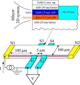
Our samples are grown by solid source molecular beam epitaxy on semi-insulating GaAs (100) substrates. The bilayer is composed of two, 12.5-nm thick InAs and 10-nm thick GaSb, quantum wells (for electrons and holes, respectively), sandwiched between two 50-nm thick AlSb barriers. Details on the growth parameters can be found elsewhere growth . As obtained from standard magnetoresistance measurements, the 2D system is characterized by bulk hole-type conductivity. The mobility at 4K is about cm2/Vs and the carrier density is cm-2.
A sample sketch is presented in Fig. 1. The 100 m wide mesa is formed by wet chemical etching. To realize transparent interfaces with a superconductor, etching is stopped just after the bottom InAs quantum well (80 nm mesa step samples), or even before it (60 nm mesa step samples). Ohmic contacts are made by thermal evaporation of 100 nm Au film. They are characterized by a constant, bias-independent resistance.
Since the edge effects are of primary importance in InAs/GaSb bilayers gasb3 ; gasb1 ; gasb2 ; gasb4 ; gasb5 ; gasb6 ; su-gasb1 ; su-gasb2 ; su-gasb3 , we fabricate side superconductor-normal (NS) junctions nbhgte ; nbsemi by sputtering 50 nm thick Nb or NbN film over the mesa step, see Fig. 1. The surface is mildly cleaned by Ar plasma. To avoid mobility degradation, the sample is kept at room temperature during the sputtering. The 10 m wide electrodes are formed by lift-off technique. This produces NS junctions with low, below , resistance. The junctions are not sensitive to low lithography misalignments, because the upper AlSb layer is an insulator at low temperatures. However, the side Nb contact is mostly connected to the bottom (electron) InAs layer. This is obvious for the 60 nm mesa step sample, where this layer is not removed. It is also the case for the photolithographically fabricated contacts to the 80 nm mesa step sample, because the common developer etches selectively the GaSb layer gasb-etching .
We study current through the Nb-InAs/GaSb junction in a four-point technique. An example of electrical connections is presented in Fig. 1: one superconducting electrode (S1) is grounded; a current is fed through the normal Ohmic contact N1; we measure a voltage drop between another superconducting electrode S2 and the ground lead (S1). In this connection scheme, a wire to the grounded superconducting S1 contact is excluded, which is necessary for low-impedance NS junctions.
To obtain characteristics, which are presented in Fig. 2, we sweep the dc current and measure the voltage drop in a mV range. To accurately determine critical current values , presented in Fig. 3, we simultaneously measure characteristics: the dc current is additionally modulated by a low ac component (10 nA, 1 kHz), the ac component of () is detected by a lock-in amplifier. We have checked, that the lock-in signal is independent of the modulation frequency in the 600 Hz – 3000 Hz range, which is defined by applied ac filters.
To extract features specific to the InAs/GaSb bilayer, the measurements are performed at low temperature of 30 mK. Because of similar critical temperature for Nb and NbN films (9 K and 11 K, respectively, both mK), the samples demonstrate even quantitatively similar behavior. However, Nb contacts are preferable, since the much lower niobium critical field T allows to distinguish between the bulk and interface effects, see Fig. 2 (e). We will concentrate on these niobium samples below.
III Experimental results
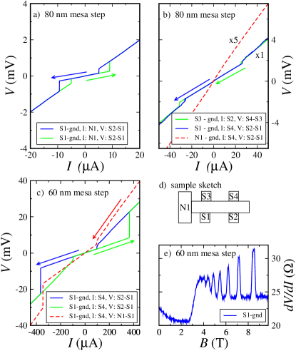
Fig. 2 (a-c) presents examples of the characteristics in zero magnetic field for the 80 nm (a,b) and 60 nm (c) mesa step samples.
The curves in Fig. 2 (a) are obtained in the electrical connection scheme, which is depicted in Fig. 1. They demonstrate Josephson-like behavior tinkham : two sharp jumps appear at A, the exact jumps’ positions are subjected to hysteresis with the sweep direction (blue and green curves). However, unlike the standard Josephson behavior tinkham , the voltage drop is not zero between the jumps.
In our four-point connection scheme, a wire to the grounded superconducting Nb contact is excluded, see Fig. 1. Thus, it can not be responsible for the non-zero slope between the jumps in Fig. 2 (a). On the other hand, the slope corresponds to resistance, which is comparable with the sheet 2D bilayer resistance at present concentration and mobility.
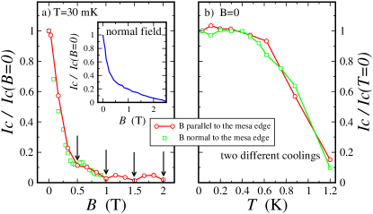
Fig. 2 (b) demonstrates that the experimental s are indeed sensitive to the current distribution within the 2D plane. Two (green and blue) curves are obtained in two symmetric contact configurations, when the current and voltage probes are placed at the opposite sample edges. The curves coincide well, because of symmetric current distribution, but differ strongly from ones in Fig. 2 (a): the jumps’ positions are placed at A and the slope between them corresponds to .
The non-zero voltage at low currents in Fig. 2 is inconsistent with the (edge or bulk) Josephson supercurrent between the superconducting potential contacts. Instead, it seems that the jumps on the experimental s originate from a single (grounded) Nb-InAs/GaSb junction, which is connected in-series with a part of the 2D bilayer system. This behavior is still induced by proximity with a superconductor: if the normal (N1) contact is grounded instead of the niobium one, is of linear Ohmic behavior, see the red dashed line in Fig. 2 (b). We can expect even stronger proximity effect for the sample with lower (60 nm) mesa step, because the bottom InAs layer is efficiently contacted to the side Nb electrode in this case. In the experiment, the jumps are situated at approximately 10 times higher current, see Fig. 2 (c).
To our surprise, the curve demonstrates the same behavior if the voltage is taken from the normal contact N1, which is 100 m separated from the grounded superconducting contact S1, see the red dashed curve in Fig. 2 (c). Thus, the jumps on the experimental s reflect transport properties of a single (grounded) Nb-InAs/GaSb junction.
Since the behavior in Fig. 2 is induced by superconductivity, it can be suppressed by a magnetic field or temperature.
The slope at zero current demonstrates strong increase near the niobium superconducting critical field =2.5 T, as demonstrated in Fig. 2 (e) for the 60 nm mesa step sample in normal magnetic field. In higher magnetic fields, well-developed Shubnikov-de-Haas magnetoresistance oscillations appear. The latter is a fingerprint of a 2D conducting system, so the curves in Fig. 2 reflect charge transport through the InAs/GaSb bilayer to the side superconducting Nb contact.
Suppression of the critical (jump) current is sensitive to the magnetic field orientation, see Fig. 3 (a). The oscillations in with equal T period are observed if the magnetic field is oriented within the 2D plane, either normal (green squares) or parallel (red circles) to the mesa edge. It is worth to mention, that the oscillatory pattern in Fig. 3 (a) even qualitatively differs from the Fraunhofer one su-gasb1 , which is another argument against the Josephson effect. In contrast, is diminishing slower, without any sign of oscillations, in the magnetic field which is normal to the 2D plane, see inset to Fig. 3 (a).
For the 80 nm mesa step sample, weakly depends on temperature at low K, but sharply falls to zero at higher 0.5 K1.2 K, see Fig. 3 (b). There is only slow (within 5%) dependence below 1.2 K for the 60 nm mesa step sample. Because of the same niobium superconductor, the experimental s seems to be defined by the proximity-induced gap at the Nb-InAs/GaSb interface.
IV Discussion
Above, we present the experimental argumentation that the observed curves are not connected with the Josephson effect. We can also support this conclusion by data known from literature su-gasb1 ; su-gasb2 ; su-gasb3 . The transition from the bulk to edge Josephson supercurrent was reported in Ref. su-gasb1, . The critical current value was about 50 nA for two 400 nm spaced, 4 m wide electrodes. This value is in 1000 times smaller than our for electrodes of similar width, separated by 5 m distance. Thus, our numerical parameters are inconsistent with the Josephson effect. On the other hand, sharp jumps were reported at high A in Ref. su-gasb2, for a single Ta-InAs/GaSb junction, the differential resistance was finite between the jumps. This behavior was out of focus of Ref. su-gasb2, , because was identified as a critical current in the superconducting Ta lead. We wish to mention here, that depends on the carrier concentration in the InAs/GaSb bilayer in Fig. 1 of Ref. su-gasb2, , so it more likely should be connected with transport within the InAs/GaSb bilayer.
We show below from our experimental dependencies, that the observed in Fig. 2 curves reflect the interlayer current near the edge of an InAs/GaSb double quantum well in proximity with a superconductor.
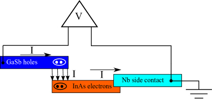
The bulk of the sample is characterized by hole-type conductivity. By approaching the edge, the hole concentration is gradually diminishing, because holes screen the edge potential shklovskii ; image02 . In other words, the edge potential is equivalent to the local gate shklovskii ; image02 , so both electron and hole layers are conducting near the edge. The side Nb contact is mostly connected to the bottom (electron) layer, see Fig. 4. This is obvious for the 60 nm mesa step sample, but it is also the case for the photolithographically fabricated contacts to the 80 nm mesa step sample, because the common developer etches selectively the GaSb layer gasb-etching .
Thus, the experimental curve reflects not only in-series connected resistances of the 2D hole layer and the Nb-InAs interface, but also the interlayer charge transfer in the vicinity of the Nb contact, see Fig. 4. The latter term is dominant for the transparent interface and high mobility holes. The proximity induced superconductivity can efficiently couple electron and hole layers due to the Cooper pair transfer. Thus, at low currents the experimental curve reflects the in-plane resistance of the 2D hole gas. The sharp jumps at high are defined by the destruction of the coherent interlayer Cooper pair transport. This situation is different from the proposals of Refs. bilayer_theor , where interlayer coupling occurs due to the exciton condensate formation.
The proposed interpretation explains why the experimental s are sensitive to the current distribution within the 2D plane in Fig. 2 (a) and (b). It is also strongly confirmed by the dependencies on the mesa step hight and temperature.
(i) For the 60 nm mesa step sample, the bottom InAs layer is efficiently contacted to the side Nb electrode, which results in the maximum proximity effect. The deeper the mesa etching, the lower the area of the Nb-InAs contact, and, therefore tinkham ; BTK , lower the induced superconductivity. It results in lower for the 80 nm mesa step sample in Fig. 2.
(ii) The induced superconducting gap can be estimated for the interlayer transport region from the temperature dependence of . From Fig. 3 (b), is about 1.3 K for the 80 nm mesa step sample. Since there is only slow (within 5%) dependence below 1.2 K for the 60 nm mesa step sample, is close to the bulk value 9 K in this case.
The periodic suppression of by magnetic field is more complicated. The oscillations in suppose a magnetic flux penetration through the closed loop. It seems to be possible in the geometry of Fig. 4 if the magnetic field is oriented along the mesa edge. The field induces a phase difference between the electron and hole layers, which results in the oscillations. The experimentally observed period T in Fig. 3 (a) corresponds () to the effective area . If we assume the effective layers’ spacing as 10 nm, the lateral dimension of the edge region in Fig. 4 can be estimated as m. This value is consistent with the proximity-induced superconductivity, because of the niobium coherence length m. The region of coherent interlayer current is of the axial symmetry near a side Nb contact, so the oscillations could be expected for any magnetic field orientation within the 2D plane. However, the interlayer phase difference does not occur in normal magnetic field, so we observe monotonous suppression of in the inset to Fig. 3 (a).
V Conclusion
As a conclusion, we investigate charge transport through the junction between a niobium superconductor and the edge of a two-dimensional electron-hole bilayer, realized in an InAs/GaSb double quantum well. For the transparent interface with a superconductor, we demonstrate that the junction resistance is determined by the interlayer charge transfer near the interface. From an analysis of experimental curves we conclude that the proximity induced superconductivity efficiently couples electron and hole layers at low currents. The critical current demonstrates periodic dependence on the in-plane magnetic field, while it is monotonous for the field which is normal to the bilayer plane.
Acknowledgements.
We wish to thank Ya. Fominov, V.T. Dolgopolov, and T.M. Klapwijk for fruitful discussions. We gratefully acknowledge financial support by the RFBR (project No. 16-02-00405), RAS and the Ministry of Education and Science of the Russian Federation under Contract No. 14.B25.31.0007.References
- (1) S. Murakami, N. Nagaosa, S.-C. Zhang, Phys. Rev. Lett. 93, 156804 (2004).
- (2) C. L. Kane, E. J. Mele, Phys. Rev. Lett. 95, 146802 (2005).
- (3) B. A. Bernevig, S.-C. Zhang, Phys. Rev. Lett. 96, 106802 (2006).
- (4) K. Suzuki, Y. Harada, K. Onomitsu, and K. Muraki, Phys. Rev. B 87, 235311 (2013).
- (5) V. T. Dolgopolov, A. A. Shashkin, E. V. Deviatov, F. Hastreiter, M. Hartung, A. Wixforth, K. L. Campman, and A. C. Gossard Phys. Rev. B 59, 13235 (1999)
- (6) C. Liu, T. L. Hughes, X.-L. Qi, K. Wang, and S.-C. Zhang, Phys. Rev. Lett. 100, 236601 (2008).
- (7) I. Knez, R.-R. Du, and G. Sullivan, Phys. Rev. Lett. 107, 136603 (2011).
- (8) I. Knez, C. T. Rettner, S.-H. Yang, S. S. P. Parkin, L. Du, R.-R. Du, and G. Sullivan, Phys. Rev. Lett. 112, 026602 (2014).
- (9) E. M. Spanton, K. C. Nowack, L. Du, G. Sullivan, R.-R. Du, and K. A. Moler, Phys. Rev. Lett. 113, 026804 (2014).
- (10) L. Du, I. Knez, G. Sullivan, and R.-R. Du, Phys. Rev. Lett. 114, 096802 (2015).
- (11) V. S. Pribiag, A. J. A. Beukman, F. Qu, M. C. Cassidy, Ch. Charpentier, W. Wegscheider and L. P. Kouwenhoven Nature Nanotechnology 10, 593 (2015) doi:10.1038/nnano.2015.86
- (12) Wenlong Yu, Yuxuan Jiang, Chao Huan, Xunchi Chen, Zhigang Jiang, Samuel D. Hawkins, John F. Klem, and Wei Pan, Appl. Phys. Lett. 105, 192107 (2014); doi: 10.1063/1.4901965
- (13) Xiaoyan Shi, Wenlong Yu, Zhigang Jiang, B. Andrei Bernevig, W. Pan, S. D. Hawkins, and J. F. Klem, J. Appl. Phys. 118, 133905 (2015); doi: 10.1063/1.4932644
- (14) For recent reviews, see C. W. J. Beenakker, Annu. Rev. Con. Mat. Phys. 4, 113 (2013) and J. Alicea, Rep. Prog. Phys. 75, 076501 (2012).
- (15) T. Chakraborty, and P. Pietilainen, Phys. Rev. Lett. 59, 2784 (1987); D. Yoshioka, A.H. MacDonald, and S.M. Girvin, Phys. Rev. B 39, 1932 (1989); J.P. Eisenstein, G.S. Boebinger, L.N. Pfeiffer, K.W. West, and S. He, Phys. Rev. Lett. 68, 1383 (1992); Y.W. Suen, L.W. Engel, M.B. Santos, M. Shayegan, and D.C. Tsui, Phys. Rev. Lett. 68, 1379 (1992); Y.W. Suen, H.C. Manoharan, X. Ying, M.B. Santos, and M. Shayegan, Phys. Rev. Lett. 72, 3405 (1994);
- (16) S.Q. Murphy, J.P. Eisenstein, G.S. Boebinger, L.N. Pfeiffer, and K.W. West, Phys. Rev. Lett. 72, 728 (1994); T.S. Lay, Y.W. Suen, H.C. Manoharan, X. Ying, M.B. Santos, and M. Shayegan, Phys. Rev. B 50, 17725 (1994).
- (17) H.C. Manoharan, Y.W. Suen, T.C. Lay, M.B. Santos, and M. Shayegan, Phys. Rev. Lett., vol. 79, p. 2722 (1997).
- (18) V. S. Khrapai, E. V. Deviatov, A. A. Shashkin, V. T. Dolgopolov, F. Hastreiter, A. Wixforth, K. L. Campman, and A. C. Gossard, Phys. Rev. Lett. 84, 725 (2000).
- (19) I. B. Spielman, J. P. Eisenstein, L. N. Pfeiffer, and K. W. West, Phys. Rev. Lett. 84, 5808 (2000).
- (20) I. B. Spielman, J. P. Eisenstein, L. N. Pfeiffer, and K. W. West, Phys. Rev. Lett. 87, 036803 (2001).
- (21) J. P. Eisenstein and A. H. MacDonald, Nature (London) 432, 691 (2004) and works cited therein.
- (22) F. Dolcini, D. Rainis, F. Taddei, M. Polini, R. Fazio, and A. H. MacDonald, Phys. Rev. Lett. 104, 027004 (2010); S. Peotta, M. Gibertini, F. Dolcini, F. Taddei, M. Polini, L. B. Ioffe, R. Fazio, and A. H. MacDonald, Phys. Rev. B 84, 184528 (2011).
- (23) M. Veldhorst, M. Hoek, M. Snelder, H. Hilgenkamp, A. A. Golubov, and A. Brinkman, Phys. Rev. B 90, 035428 (2014).
- (24) E.A. Emel’yanov, D.F. Feklin, A.V. Vasev, M.A. Putyato, B.R. Semyagin, A.P. Vasilenko, O.P. Pchelyakov, V.V. Preobrazhenskii, Optoelectronics, Instrumentation and Data Processing, 47, 452 (2011).
- (25) A. Kononov, S. V. Egorov, N. Titova, Z. D. Kvon, N. N. Mikhailov, S. A. Dvoretsky, E. V. Deviatov, JETP Lett., 101 , 41 (2015).
- (26) A. Kononov, S. V. Egorov, Z. D. Kvon, N. N. Mikhailov, S. A. Dvoretsky, and E. V. Deviatov, Phys. Rev. B 93, 041303(R) (2016)
- (27) F. Rahman, B. L. Gallagher, M. Behet, and J. De Boeck, Appl. Phys. Lett. 73, 88 (1998); doi: 10.1063/1.121789
- (28) M. Tinkham, Introduction to Superconductivity (2d ed., McGraw–Hill, New York, 1996).
- (29) G.E. Blonder, M. Tinkham, T.M. Klapwijk, Physical Review B, 25, 4515 (1982).
- (30) D. B. Chklovskii, B. I. Shklovskii, and L. I. Glazman, Phys. Rev. B 46, 4026 (1992).
- (31) E. Ahlswede, J. Weis, K. v. Klitzing, K. Eberl, Physica E, 12, 165 (2002).