Photon-Induced Selenium Vacancies in TiSe2
Abstract
TiSe2 is a member of transition metal dichalcogenide family of layered van-der-Waals materials that exhibits some distinctive electronic and optical properties. Here, we perform Raman spectroscopy studies on single crystal TiSe2 to investigate photon-induced defects associated with formation of selenium vacancies. Two additional Eg phonon peaks are observed in the laser-irradiated regions, consistent with Raman spectra of selenium deficient TiSe2. Temperature dependent studies of the threshold laser intensity necessary to form selenium vacancies show that there is a linear dependence. We extract the relevant activation energy for selenium vacancy nucleation. The impact of these results on the properties of strongly correlated electron states in TiSe2 are discussed.
pacs:
68.35.Dv, 61.72.Cc, 61.80.Ba, 77.84.BwTransition metal dichalcogenides (TMDs) exhibit series of unique electronic properties ranging from charge density wave (CDW) order to superconductivity. 1T-TiSe2 is a quasi-2D layered material with a trigonal symmetry that has been studied for over 30 years Di Salvo, Moncton, and Waszczak (1976); Wilson (1978); Guo et al. (2015); Lorchat, Froehlicher, and Berciaud (2016); Cercellier et al. (2007); Monney et al. (2010); Fogler, Butov, and Novoselov (2014); Korn et al. (2011); Bhatt et al. (2013). Only recently it was discovered that the CDW in this material has excitonic origin Cercellier et al. (2007); Monney et al. (2010) and a chiral order, Ishioka et al. (2010); Castellan et al. (2013) which might have implications on fundamental understanding of the strongly correlated electron systems. On the other hand, the ability to separate charges in materials with reduced dimensionality is of great interest for many potential applications. Fogler, Butov, and Novoselov (2014); Korn et al. (2011) Due to its specific structural and electronic properties TiSe2 has also been considered as alternative to graphene electronics, Chen et al. (2015); Li et al. (2016a) in thermoelectric applications Bhatt et al. (2014, 2013) and as a cathode material in batteries. Gu et al. (2015)
The strongly correlated electron behavior in TMDs is usually attributed to their quasi-two-dimensional structure consisting of -- layers (transition metal and chalcogen) weakly bound together by van der Waals forces. Lv et al. (2015) Further interest in these systems has been stimulated by the changes in their bulk electronic properties upon reduction to a single monolayer. The modification of the electronic properties in 2D layered systems is due to the changes in the electronic and phonon band structure when the systems are reduced to a single -- layer. Zhu, Cheng, and Schwingenschlogl (2011); Lebegue and Eriksson (2009) Fabrication of single or few layer TMDs proceeds either by exfoliation from single crystals Ubaldini and Giannini (2014); Li et al. (2016a) or through chemical growth of thin films. Peng et al. (2015); Boscher, Carmalt, and Parkin (2006); Sugawara et al. (2016) The first method has been favored by many researchers ever since it was first used with graphene, as it tends to yield better crystalline quality and, therefore, is very suitable for studying the fundamental physical properties. However, exfoliation is not scalable, making it ill-suited for device fabrication and integration with other thin film materials and processes.
On the other hand, physical and chemical vapor deposition methods are very flexible in terms of control of thickness and chemical composition of the dichalcogenide layers. Up to now TiSe2 monolayers have proven difficult to obtain through methods other than molecular beam epitaxy. Sugawara et al. (2016) Synthesized thin film TMDs often suffer from high concentration of defects and lack of long range crystalline order Lv et al. (2015). In TiSe2 the most frequent defects are selenium vacancies Di Salvo, Moncton, and Waszczak (1976); Hildebrand et al. (2014). The concentration of selenium vacancies depends strongly on the conditions of film growth, especially growth temperature, similar as in the case of single crystal growth Di Salvo, Moncton, and Waszczak (1976); Wilson (1978). Selenium deficiencies are often detrimental to the charge density wave order Lv et al. (2015) as their presence changes the nature of the material from semiconducting to semimetallic. Therefore, the characterization of the defects and their dynamics is of utmost importance.
Raman spectroscopy is one of the main tools utilized to study layered TMDs, as the symmetric A1g breathing phonon mode and Eg layer shearing mode are sensitive to inter- and intra-layer properties of the structure. Zhao et al. (2011) As in the case of graphene, Raman spectra can distinguish between single and few layers of TMD on the surface. Indeed, both resonant and non-resonant Raman spectroscopy has already been used to distinguish multilayered thin films of MoS2, Soubelet et al. (2016) WS2, Staiger et al. (2015) MoTe2, Guo et al. (2015) and other members of the TMD family. Lorchat, Froehlicher, and Berciaud (2016) In the present work we study the evolution of selenium vacancies in high quality TiSe2 single crystals as they appear in Raman spectra through Raman laser induced vaporization of the selenium atoms. The temperature dependent studies allow us to estimate the activation energy for selenium vacancy nucleation, an important parameter if considering TiSe2 as material for electronic and optical applications.
High quality single crystals of TiSe2 were grown using chemical vapor transport method Di Salvo, Moncton, and Waszczak (1976); Oglesby et al. (1994); Wilson (1978) and characterized using EDS, XRD and variable temperature electrical transport. One of the signatures of low level of intrinsic defects in the single crystals is the high charge density peak in resistivity at the CDW transition (2.5–3.5 times the room temperature resistivity) and low level of defect concentration as observed by scanning tunneling microscopy Iavarone et al. (2012). Variable temperature Raman spectroscopy measurements were conducted at the Center for Nanoscale Materials at Argonne National Laboratory using a Renishaw InVia Raman microscope with a 514 nm argon ion laser source and a 1.5 m diameter spot size. The spectrometer is equipped with variable temperature cell capable of operating between 80–400 K. All the experiments were conducted in the presence of ultra-high pure nitrogen exchange gas at normal pressure.
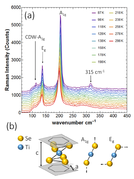
Fig. 1a shows Raman spectra on freshly cleaved surface of TiSe2 single crystal. At room temperature one can see the normal phase shearing mode Eg and breathing mode A1g peaks. As the temperature is lowered below the CDW transition of 200 K we see the emergence of additional peaks that reflect the change in lattice symmetry. The CDW doubles the period of the crystal lattice to 2a2a2c and induces additional Raman peaks: the 315 cm-1 peak is first seen below 160 K, in agreement with previous measurements. Snow et al. (2003); Sugai et al. (1980); Holy et al. (1977) The charge density wave A1g peak at 110 cm-1 becomes fully observable only at temperatures lower than 100K. Barath et al. (2008)
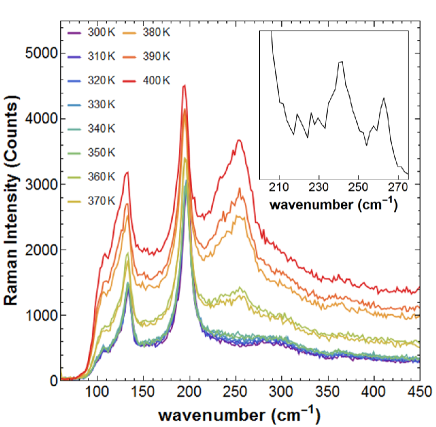
Uniform heating of the TiSe2 single crystal above room temperature makes the crystal structure more susceptible to laser induced change. Fig. 2 shows the evolution of Raman spectra of the TiSe2 single crystal from room temperature and up to 400 K. At 300 K one notices a broad Raman background signal centered at around 250 cm-1. There are also enhanced fluctuations of the background intensity in the spectrum around this frequency. As the the temperature is increased, the broad background slowly evolves into a set of distinct peaks. At 360 K we observe a broad increase in the background at near 250 cm-1. This broad peak is consistent with previous Raman experiments performed on non-stoichiometric TiSe2-x with high concentration of selenium vacancies. Bhatt et al. (2014) As the temperature is raised further, the broad background evolves into distinct peaks that are made up of two Raman modes centered at 241 and 263 cm-1. They are shown in the inset of Fig.2 and were obtained by reducing the laser power from 1.87 mW to 1.05 mW and moving the laser spot outside the perimeter of the original beam profile. The result indicates that high beam powers damage the sample surface within the laser beam profile, and within a much larger radius ( 100 m depending on the excitation power) some of the surface selenium atoms sublime leaving selenium vacancies on the TiSe2 single crystal surface.
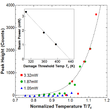
To understand the relevant temperatures and activation energies for nucleation of selenium vacancies we conducted systematic experiments by varying both laser beam power and temperature. Each measurement was made on large atomically flat planes of the single crystal surface with no edges in the microscope image. Raman spectrum at each temperature was taken for 3 min before blocking the laser beam and moving on to the next higher temperature setpoint. Each spectrum was taken on a different and pristine location on the surface of the single crystal in order to avoid effects from previous laser irradiation. In Fig. 3 Raman intensity at 253 cm-1 is plotted versus temperature for multiple beam powers, each showing different onset of the peak increase with temperature. The threshold temperature beyond which the peak height at 253 cm-1 starts increasing marks the onset of irreversible damage done to the crystal surface. The inset in Fig. 3 shows a linear relationship between the beam power and threshold temperature Tc for irreversible damage, suggesting that thermal effects are responsible for selenium vaporization. The extrapolation of the curve to vanishing laser power leads to zero crossing at 435 K. This suggest of a relatively low temperature threshold at which the process of generation of selenium vacancies starts taking place. Since this process is thermally activated, we fit the peak height vs normalized temperature with Arrhenius dependence and find that the activation energy for selenium vacancy generation is 0.52 eV. Our results of laser damage of TiSe2 single crystals very much resemble the experiments on CdZnTe in which the processes of evaporation of cadmium and migration of tellurium to the damaged sites takes place due to the laser-surface interaction. Hawkins et al. (2008); Teague et al. (2009)
The results on the photon induced nucleation of selenium vacancies in TiSe2 have broader implications for both fundamental studies of TiSe2 as well as potential practical applications. The interest in TiSe2 dichalcogenide has been due to its excitonic nature of charge density wave state, superconductivity in CuxTiSe2 Morosan et al. (2006) and PdxTiSe2, Morosan et al. (2010) as well as due to unique observation of the chiral charge density waves. Fundamental studies of these correlated states and their coexistence have been on the rise recently, as the dichalcogenide system is structurally relatively simple and can provide some answers in regards to the mechanisms of correlated electron states in other classes of materials like perovskite high temperature superconductors or pnictides. Since TiSe2 is a compensated semimetal with very large Hall coefficient at low temperatures Di Salvo, Moncton, and Waszczak (1976), the correlated electron states are very susceptible to the level of intrinsic doping. Therefore, any fundamental studies should take into account the selenium vacancy concentration levels and the relatively low activation energy for their nucleation Novello et al. (2015). The concentration and dynamics of selenium vacancies could be very important in TiSe2 thin films Goli et al. (2012); Li et al. (2016a); Peng et al. (2015) as the Raman peaks associated with these defects are strong in synthesized films Goli et al. (2012); Bhatt et al. (2014). With reduced dimensionality of the system (from 3D crystals to 2D thin films), the activation energy for selenium vacancy formation could further decrease and make the 2D system metastable even at room temperatures. The intrinsic doping due to vacancies might suppress the charge density wave correlations and reduce the signature of charge density wave phase normally observed resistivity vs temperature measurements Goli et al. (2012). A possible method to prevent selenium vaporization and at the same time enhance the CDW transition temperature in 2D TiSe2 could be the encapsulation using hexagonal boron nitride, as shown recently. Li et al. (2016b) Clearly, more work needs to be done in this area to understand the dynamics of selenium in TiSe2 and with recent advances in tip-enhanced Raman spectroscopy Jiang et al. (2016) one could possibly obtain sufficient spatial and spectroscopic resolution.
Raman spectroscopy studies on single crystal TiSe2 show a photon-induced defect signature associated with nucleation of selenium vacancies. Two additional Eg phonon peaks at 241 and 263 cm-1 are observed in the laser irradiated regions, consistent with Raman spectra of selenium deficient TiSe2. Temperature dependent studies of the threshold laser intensity necessary to form selenium vacancies show that there is a linear dependence, suggesting thermally activated character of the process. The extrapolation of the onset temperature of the photon-induced damage shows that the process of selenium vacancy nucleation could start at temperatures as low as 435 K without the assistance of any photon sources.
Acknowledgements.
We would like to acknowledge the support by National Science Foundation under Grant No. ECCS-1408151. The use of the Center for Nanoscale Materials, an Office of Science user facility, was supported by the U. S. Department of Energy, Office of Science, Office of Basic Energy Sciences, under Contract No. DE-AC02-06CH11357.References
- Di Salvo, Moncton, and Waszczak (1976) F. J. Di Salvo, D. E. Moncton, and J. V. Waszczak, Phys. Rev. B 14, 4321 (1976).
- Wilson (1978) J. A. Wilson, Phys. Status Solidi B 86, 11 (1978).
- Guo et al. (2015) H. Guo, T. Yang, M. Yamamoto, L. Zhou, R. Ishikawa, K. Ueno, K. Tsukagoshi, Z. Zhang, M. S. Dresselhaus, and R. Saito, Phys. Rev. B 91, 205415 (2015).
- Lorchat, Froehlicher, and Berciaud (2016) E. Lorchat, G. Froehlicher, and S. Berciaud, ACS Nano 10, 2752 (2016).
- Cercellier et al. (2007) H. Cercellier, C. Monney, F. Clerc, C. Battaglia, L. Despont, M. G. Garnier, H. Beck, P. Aebi, L. Patthey, H. Berger, and L. Forro, Phys. Rev. Lett. 99, 146403 (2007).
- Monney et al. (2010) C. Monney, E. F. Schwier, M. G. Garnier, N. Mariotti, C. Didiot, H. Cercellier, J. Marcus, H. Berger, A. N. Titov, H. Beck, and P. Aebi, New J. Phys. 12, 125019 (2010).
- Fogler, Butov, and Novoselov (2014) M. M. Fogler, L. V. Butov, and K. S. Novoselov, Nature Commun. 5, 4555 (2014).
- Korn et al. (2011) T. Korn, S. Heydrich, M. Hirmer, J. Schmutzler, and C. Schueller, Appl. Phys. Lett. 99, 102109 (2011).
- Bhatt et al. (2013) R. Bhatt, R. Basu, S. Bhattacharya, A. Singh, D. K. Aswal, S. K. Gupta, G. S. Okram, V. Ganesan, D. Venkateshwarlu, C. Surgers, M. Navaneethan, and Y. Hayakawa, Appl. Phys. A-Materials Science and Processing 111, 465 (2013).
- Ishioka et al. (2010) J. Ishioka, Y. H. Liu, K. Shimatake, T. Kurosawa, K. Ichimura, Y. Toda, M. Oda, and S. Tanda, Phys. Rev. Lett. 105, 176401 (2010).
- Castellan et al. (2013) J.-P. Castellan, S. Rosenkranz, R. Osborn, Q. Li, K. E. Gray, X. Luo, U. Welp, G. Karapetrov, J. P. C. Ruff, and J. van Wezel, Phys. Rev. Lett. 110, 196404 (2013).
- Chen et al. (2015) P. Chen, Y. H. Chan, X. Y. Fang, Y. Zhang, M. Y. Chou, S. K. Mo, Z. Hussain, A. V. Fedorov, and T. C. Chiang, Nature Commun. 6, 8943 (2015).
- Li et al. (2016a) L. J. Li, E. C. T. O’Farrell, K. P. Loh, G. Eda, B. Ozyilmaz, and A. H. C. Neto, Nature 529, 185 (2016a).
- Bhatt et al. (2014) R. Bhatt, S. Bhattacharya, R. Basu, S. Ahmad, A. K. Chauhan, G. S. Okram, P. Bhatt, M. Roy, M. Navaneethan, Y. Hayakawa, A. K. Debnath, A. Singh, D. K. Aswal, and S. K. Gupta, ACS Appl. Mater. Interfaces 6, 18619 (2014).
- Gu et al. (2015) Y. Gu, Y. Katsura, T. Yoshino, H. Takagi, and K. Taniguchi, Sci. Rep. 5, 12486 (2015).
- Lv et al. (2015) R. Lv, J. A. Robinson, R. E. Schaak, D. Sun, Y. Sun, T. E. Mallouk, and M. Terrones, Acc. Chem. Res. 48, 56 (2015).
- Zhu, Cheng, and Schwingenschlogl (2011) Z. Y. Zhu, Y. C. Cheng, and U. Schwingenschlogl, Phys. Rev. B 84, 153402 (2011).
- Lebegue and Eriksson (2009) S. Lebegue and O. Eriksson, Phys. Rev. B 79, 115409 (2009).
- Ubaldini and Giannini (2014) A. Ubaldini and E. Giannini, J. Cryst. Growth 401, 878 (2014).
- Peng et al. (2015) J.-P. Peng, J.-Q. Guan, H.-M. Zhang, C.-L. Song, L. Wang, K. He, Q.-K. Xue, and X.-C. Ma, Phys. Rev. B 91, 121113(R) (2015).
- Boscher, Carmalt, and Parkin (2006) N. D. Boscher, C. J. Carmalt, and I. P. Parkin, Chem. Vap. Deposition 12, 54 (2006).
- Sugawara et al. (2016) K. Sugawara, Y. Nakata, R. Shimizu, P. Han, T. Hitosugi, T. Sato, and T. Takahashi, ACS Nano 10, 1341 (2016).
- Hildebrand et al. (2014) B. Hildebrand, C. Didiot, A. M. Novello, G. Monney, A. Scarfato, A. Ubaldini, H. Berger, D. R. Bowler, C. Renner, and P. Aebi, Phys. Rev. Lett. 112, 197001 (2014).
- Zhao et al. (2011) W. Zhao, P. H. Tan, J. Liu, and A. C. Ferrari, J. Am. Chem. Soc. 133, 5941 (2011).
- Soubelet et al. (2016) P. Soubelet, A. E. Bruchhausen, A. Fainstein, K. Nogajewski, and C. Faugeras, Phys. Rev. B 93, 155407 (2016).
- Staiger et al. (2015) M. Staiger, R. Gillen, N. Scheuschner, O. Ochedowski, F. Kampmann, M. Schleberger, C. Thomsen, and J. Maultzsch, Phys. Rev. B 91, 195419 (2015).
- Oglesby et al. (1994) C. S. Oglesby, E. Bucher, C. Kloc, and H. Hohl, J. Cryst. Growth 137, 289 (1994).
- Iavarone et al. (2012) M. Iavarone, R. Di Capua, X. Zhang, M. Golalikhani, S. A. Moore, and G. Karapetrov, Phys. Rev. B 85, 155103 (2012).
- Snow et al. (2003) C. S. Snow, J. F. Karpus, S. L. Cooper, T. E. Kidd, and T. C. Chiang, Phys. Rev. Lett. 91, 136402 (2003).
- Sugai et al. (1980) S. Sugai, K. Murase, S. Uchida, and S. Tanaka, Solid State Commun. 35, 433 (1980).
- Holy et al. (1977) J. A. Holy, K. C. Woo, M. V. Klein, and F. C. Brown, Phys. Rev. B 16, 3628 (1977).
- Barath et al. (2008) H. Barath, M. Kim, J. F. Karpus, S. L. Cooper, P. Abbamonte, E. Fradkin, and R. J. Cava, Phys. Rev. Lett. 100, 106402 (2008).
- Hawkins et al. (2008) S. A. Hawkins, E. Villa-Aleman, M. C. Duff, D. B. Hunter, A. Burger, M. Groza, V. Buliga, and D. R. Black, J. Electron. Mater. 37, 1438 (2008).
- Teague et al. (2009) L. C. Teague, S. A. Hawkins, M. C. Duff, M. Groza, V. Buliga, and A. Burger, J. Electron. Mater. 38, 1522 (2009).
- Morosan et al. (2006) E. Morosan, H. W. Zandbergen, B. S. Dennis, J. W. G. Bos, Y. Onose, T. Klimczuk, A. P. Ramirez, N. P. Ong, and R. J. Cava, Nature Phys. 2, 544 (2006).
- Morosan et al. (2010) E. Morosan, K. E. Wagner, L. L. Zhao, Y. Hor, A. J. Williams, J. Tao, Y. Zhu, and R. J. Cava, Phys. Rev. B 81, 094524 (2010).
- Novello et al. (2015) A. M. Novello, B. Hildebrand, A. Scarfato, C. Didiot, G. Monney, A. Ubaldini, H. Berger, D. R. Bowler, P. Aebi, and C. Renner, Phys. Rev. B 92, 081101(R) (2015).
- Goli et al. (2012) P. Goli, J. Khan, D. Wickramaratne, R. K. Lake, and A. A. Balandin, Nano Lett. 12, 5941 (2012).
- Li et al. (2016b) L. J. Li, W. J. Zhao, B. Liu, T. H. Ren, G. Eda, and K. P. Loh, Appl. Phys. Lett. 109, 141902 (2016b), 10.1063/1.4963885.
- Jiang et al. (2016) N. Jiang, D. Kurouski, E. A. Pozzi, N. Chiang, M. C. Hersam, and R. P. V. Duyne, Chem. Phys. Lett. 659, 16 (2016).