A tunable electronic beam splitter realized with crossed graphene nanoribbons
Abstract
Graphene nanoribbons (GNRs) are promising components in future nanoelectronics due to the large mobility of graphene electrons and their tunable electronic band gap in combination with recent experimental developments of on-surface chemistry strategies for their growth. Here we explore a prototype 4-terminal semiconducting device formed by two crossed armchair GNRs (AGNRs) using state-of-the-art first-principles transport methods. We analyze in detail the roles of intersection angle, stacking order, inter-GNR separation, and finite voltages on the transport characteristics. Interestingly, when the AGNRs intersect at , electrons injected from one terminal can be split into two outgoing waves with a tunable ratio around 50% and with almost negligible back-reflection. The splitted electron wave is found to propagate partly straight across the intersection region in one ribbon and partly in one direction of the other ribbon, i.e., in analogy of an optical beam splitter. Our simulations further identify realistic conditions for which this semiconducting device can act as a mechanically controllable electronic beam splitter with possible applications in carbon-based quantum electronic circuits and electron optics. We rationalize our findings with a simple model that suggests that electronic beam splitters can generally be realized with crossed GNRs.
I Introduction
The wave nature of electrons that propagate coherently in ballistic, one-dimensional conductors has certain qualities in common with photons propagating in vacuum.Bocquillon et al. (2014) This analogy has spawned the field of electron quantum optics, in which a number of optical setups have been realized in form of their electronic counterparts, such as the Hanbury Brown and Twiss geometry for studies of Fermion anti-bunching Henny et al. (1999); Oliver et al. (1999) and the two-particle Aharanov-Bohm effect Samuelsson et al. (2004); Neder et al. (2007); Splettstoesser et al. (2010) as well as Mach–Zehnder interferometry with charged quasiparticles Ji et al. (2003); Roulleau et al. (2007). The advent of coherent single-particle sources Fève et al. (2007); Dubois et al. (2013); Bocquillon et al. (2013); Waldie et al. (2015); Ryu et al. (2016) and entangled electron pair generatorsHofstetter et al. (2009); Ubbelohde et al. (2014) has further provided exciting possibilities for novel quantum technologies and information processing.
A fundamental component for such electron quantum optics is the need for semi-transparent “mirrors”, i.e., electronic beam splitters. Currently, most experimentsBocquillon et al. (2014) rely on mesoscopic devices based on high-mobility two-dimensional electron gases in the quantum Hall effect regime, in which the electron transport occurs by chiral edge channels that are generally protected against backscattering. A beam splitter is here realized with a quantum point contact that is tuned via electrostatic gates such that only one quantum transport channel transmits with probability . However, a drawback of the technology in quantum Hall regime is the need for low temperatures and high magnetic fields which severely limits possible applications outside of the laboratory.
Graphene nanoribbons (GNRs) Fujita et al. (1996); Nakada et al. (1996); Wakabayashi et al. (1999) have some highly desirable properties for their use in molecular-scale electronics devices – they can be designed with specific band gaps Han et al. (2007); Son et al. (2006); Yang et al. (2007) and long defect-free samples can now be fabricated with both armchair (AGNR) Cai et al. (2010) and zigzag (ZGNR) edge topology Ruffieux et al. (2016) via on-surface synthesis. However, in the standard bottom-up approach it is difficult to fully explore the GNR electronic properties due to interactions with the metallic substrates used for the synthesis. Very recently this drawback has been bypassed using synthesis on a semi-conducting substrate Oliveira et al. (2015); Jacobberger et al. (2015) and by post-synthesis transfer to an insulating substrate Ruffieux et al. (2016). Manipulation of single GNRs have also been demonstrated with scanning probe microscopy, Koch et al. (2012); Kawai et al. (2016) which opens the possibility to built novel electronic networks with GNRs. Simple 4-terminal tunneling junctions can be fabricated by crossing 1D-structures such as carbon nanotubes Fuhrer et al. (2000); Yoon et al. (2001) or GNRs. Jiao et al. (2010) Indeed, in the context of electron quantum optics, it was very recently theoretically proposed that two crossed ZGNRs could act as an electronic beam splitter Lima et al. (2016).
The quantum transport properties of GNR-based devices have been extensively studied with first-principles methods, for instance in the contexts of chemical functionalization López-Bezanilla et al. (2009), optical excitations Osella et al. (2012); Villegas et al. (2014), thermoelectrics Tan et al. (2011); Saha et al. (2011); Sevincli et al. (2013), local current-density patterns Wilhelm et al. (2014), vibrational excitations Christensen et al. (2015), and spin-scattering in ZGNRs Kim and Kim (2008); Zeng et al. (2010, 2011) and hydrogenated AGNRs. Soriano et al. (2010); Wilhelm et al. (2015). Various multi-terminal GNR geometries have also been addressed, both in-plane GNR devices Jayasekera and Mintmire (2007); Areshkin and White (2007); Botello-Méndez et al. (2011); Xu et al. (2013) and tunneling junctions formed between GNRs. Botello-Méndez et al. (2011); Masum Habib and Lake (2012); Masum Habib et al. (2013); Saha and Nikolic (2013); Van de Put et al. (2016) Finite-bias calculations in a multi-terminal context were pioneered by Saha et al. Saha et al. (2009) and are becoming increasingly accessible in first-principles transport codes, such as the post-processing tool Gollum Ferrer et al. (2014) and the open-source, self-consistent methods of TranSiesta. Brandbyge et al. (2002); Papior et al. (2016)
In this manuscript we employ state-of-the-art first-principles methods to study the transport properties of tunneling junctions formed by two crossed AGNRs. Earlier studies have explored similar systems,Masum Habib and Lake (2012); Van de Put et al. (2016) but these did not account for the charge redistribution in the junction at finite bias. We analyze in detail the roles of intersection angle, stacking order, inter-GNR separation, and finite voltages in this effective 4-terminal device. Interestingly, we discovered that when the two AGNRs cross at an intersection angle a substantial current can be passed from one ribbon to the other and, more specifically, that electrons injected from one terminal can be split into two outgoing waves with a tunable ratio around 50% and with almost negligible back-reflection. We quantify how this inter-GNR tunneling mechanism depends on the precise atomic arrangement and demonstrate how this enables our device to be tuned and controlled to act as an electronic beam splitter. We further propose a simple model to understand qualitatively the critical role of the intersection angle, which points toward the possibility that electronic beam splitters can be realized with GNRs of different chiralities and widths. We therefore speculate that such GNR-based beam splitters could find applications in electron quantum optics at the nanoscale.
II Methodology
II.1 Multiterminal DFT-NEGF
The calculations presented here were performed using the Siesta/TranSiesta packages Soler et al. (2002); Brandbyge et al. (2002) that are based on density functional theory (DFT) and nonequilibrium Green’s functions (NEGF), a combination that is referred to as DFT-NEGF. The TranSiesta code which was recently generalized to deal with multi-terminal devices in complex geometries, i.e., to allow any number of electrodes pointing in arbitrary directions Papior et al. (2016). Following Saha et al. Saha et al. (2009), our multi-terminal system is defined by an expanded scattering region that includes the connections to the electrodes and a central region which is chosen such that any two terminals only interact through it. Each semi-infinite terminal is assumed to be in thermal equilibrium characterized by a chemical potential . The transport properties at the steady state are obtained within the NEGF approach Keldysh (1965); Kadanoff and Baym (1962) by the propagator through the scattering region which, at energy , is given by:
| (1) |
with . Here and are the scattering region overlap and Hamiltonian matrices, respectively, and the -th lead retarded self-energy that introduces the effect of connecting the -th electrode to the central region. On the one hand, when a bias voltage is applied to an electrode it is assumed that its energy levels are rigidly shifted. Therefore, each electrode has a chemical potential defined by , where is the Fermi energy of the combined system in equilibrium, is the applied bias window (the maximum absolute potential difference between any two terminals) and is a proportionality factor that defines the chemical potential of the -th electrode in terms of . The central region, on the other hand, will have the charge distribution modified due to the connection to biased electrodes, which is then determined self-consistently within the DFT-NEGF procedure Papior et al. (2016).
In a multi-terminal setup it is a non-trivial task to determine the electrostatic potential which solves the Poisson equation and fulfills the boundary conditions imposed by all electrodes. In our calculations, we use the box approximation,Papior et al. (2016) which consists of reinforcing the potential difference between the electrodes at each self-consistent step. This is done by adding the chemical potential to the periodic solution of the Poisson equation at the region belonging to the -th electrode, and with a redefinition of the common energy reference at each iteration step. The box approximation, particularly when combined with semi-conducting low-dimensional electrodes as in the present case, can potentially create an abrupt behavior of the potential at the boundaries between the electrodes and the central region. However, in the calculations presented here, only a modest charge accumulation occurs at the central-region/lead boundary. Even at the largest applied bias less than /atom accumulate at each side of the boundary, producing a negligible scattering, as demonstrated by the fact that varying the locations of the central-region/lead boundaries had only a negligible effect on the results.
Once the DFT-NEGF self-consistency is achieved, one can compute the transport properties. The current flowing out of a given electrode depends on the transmission probabilities of electrons being scattered to any of the other electrodes . This is expressed in terms of the multi-terminal Landauer-Büttiker formula Büttiker (1986):
| (2) |
where
| (3) |
is the -th electrode spectral function,
| (4) |
the level-width function, and the Fermi-Dirac distribution. The factor 2 is due to the spin degeneracy in a spin-less treatment.
Finally, to analyze the electron transport properties of multi-terminal devices in real space, we calculate the so-called bond currents Todorov (2002), i.e., the amount of current flowing from atom to . For scattering states originating from the -th electrode the bond current is defined as:
| (5) | ||||
where characterizes the energy window of interest. A summation over orbitals belonging to atoms and is implicit in Eq. (5).
II.2 Details of calculations
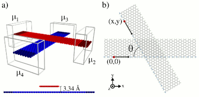
Our device, shown in Fig. 1, is comprised of two infinite H-passivated 14-AGNRs (armchair graphene nanoribbons with a width of carbon atoms) rotated by an angle with respect to each other. Each GNR in the scattering region thus bridges two semi-infinite electrodes, one on each side of the intersection i.e., the system has a total of four terminals. All calculations were therefore performed using the vdW density functional of Dion et al Dion et al. (2004) with the modified exchange by Klimeš, Bowler and Michaelides Klimeš et al. (2010) since the description of dispersive interactions is crucial to describe interlayer binding and density rearrangment. Santos et al. (2012) The core electrons were described by non-local Troullier-Martins pseudopotentials Troullier and Martins (1991) and a double- basis set was used to expand the valence-electron wavefunctions. Soler et al. (2002) The fineness of the real space grid and the orbital radii were defined using, respectively, a 350 Ry energy cutoff and a 30 meV energy shift. Soler et al. (2002)
First we allowed one ribbon, with axis along the direction, to fully relax using conjugate gradient method using a force tolerance of 5 meV/Å. The relaxed structure was then duplicated and translated along the direction by 3.34 Å (lowest energy distance for ) to explore the dependence of the transport properties on the other geometrical parameters (angle, stacking) defining our device.111Using the same functional and basis set, we found that for bilayer graphene the equilibrium distance between the two layers is 3.486 Å for an AA stacking and 3.294 Å for AB stacking. For a crossed GNR system with one GNR rotated by 90∘ with respect to the other, we found 3.339 Å as the lowest energy distance, which lies in between these two extremes values for a bilayer graphene. Moreover, the lattice parameter calculated for graphite with different stackings ( Å, Å and Å), which are in close agreement with experiment measurements of Å Baskin and Meyer (1955); Zhao and Spain (1989), also presents an interlayer distance between the bilayer graphene values for AA and AB stacking. Therefore, we found reasonable to use the distance Å as the reference value for all our crossed structures. We additionally considered the dependence of the transport properties on small variations of the distance between the ribbons.
Each GNR consists of 640 atoms in the scattering region and, altogether, the system is described by total of 9280 orbitals with the chosen basis set. The electrode region , i.e., where the -th semi-infinite lead is coupled to the system (boxes in Fig. 1a), is defined by 64 atoms and is described by a chemical potential . The system configuration (relative position and rotation) is defined by the angle between the edge vectors (black arrows at Fig. 1b) and the relative position between one reference atom and its replica. In order to uniquely define the different structures, we choose the reference atom as the fifth carbon atom along one edge (red dots at Fig. 1b). The system is thus geometrically defined by . In what follows, if only is explicitly specified then it is understood that the duplicated ribbon was rotated with respect the center of mass of the portion of the ribbon in the central region, i.e., that shown in Fig. 1.
In our simulations we considered an electronic temperature of K. For the electrode calculations we used 60 -points along the periodic direction. A level broadening of eV was considered in the electrodes, while eV was used for the contour integrations over the complex plane. Papior et al. (2016); Brandbyge et al. (2002) The self-consistency cycle was stopped when the difference between each element of the density matrix changed by less than .
III Results
Throughout the paper we will use intra-GNR to refer to events on the same ribbon (such as the transmission between electrodes belonging to the same ribbon) and inter-GNR for events involving the two different ribbons (such as the transmission from one ribbon to the other). Also, we will refer to the 14-AGNR attached to the electrodes 1 and 2 as GNR12 and, analogously, the ribbon attached to the electrodes 3 and 4 as GNR34.
III.1 Band structure and zero-bias transmission of the isolated 14-AGNR
A natural starting point for investigating the crossbar system lies in understanding the properties of a single GNR. As seen in Fig. 2a, our periodic calculations predict the 14-AGNR to be a semiconductor with a small band gap of meV, consistent with the result expected for a width of type .Son et al. (2006) This opening of the gap as compared to bulk graphene occurs due to the one-dimensional confinement. A direct correspondence between the band structure and the zero-bias transmission of a pristine 14-AGNR (Fig. 2b, dashed green line) can be made. As for any one-dimensional pristine structure of atomic-scale cross-section, the GNRs have a step-like transmission , where is the number of conductance channels (or, equivalently, number of bands) available at a given energy . Thus, for the single 14-AGNR around the Fermi level (in a range of approximately eV) we first find a small region of zero transmission, due to the gap, and a plateau of transmission 1 associated with the highest valence (VB) and lowest conduction band (CB), respectively at larger negative and positive energies. The behavior of the transmission is very symmetric with respect to middle of the band gap, reflecting the approximate electron-hole symmetry of the band structure in the system.
III.2 Effect of inter-ribbon voltage
We now start analyzing the effect of the scattering due to the interaction between the ribbons both in the intra- and inter-GNR transport characteristics. In Fig. 2b we present the intra-GNR transmissions (blue) and (dashed red line) obtained for the structure as a function of a inter-GNR voltage , i.e., the bias is applied so to create a potential difference between the two GNRs (, with and ). As mentioned above, the zero-bias transmission of a pristine 14-AGNR (dashed green) serves as a reference.
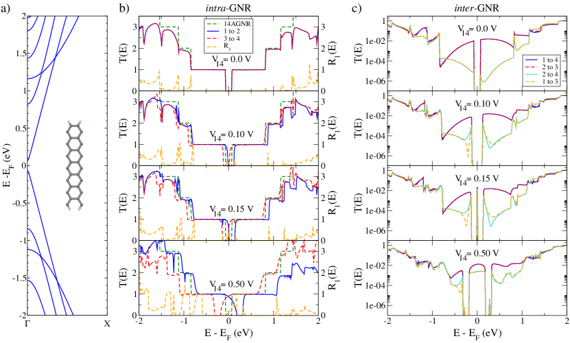
The main effect observed in the intra-GNR transmissions is a rigid shift of the ribbons’ electronic levels by . At higher energies, far from , dips on the intra-GNR transmission are observed, which are related to the increase of the backscattering probability, or reflection function, (for electrode 1 see orange dashed curves at Fig. 2b).
For the device the intra-GNR transmission is considerably larger than the inter-GNR, as can be seen in Fig. 2c (notice the logarithmic scale in this figure, see also the top panels in Fig. 3). With the increasing of bias, the major effect in the inter-GNR is a widening of the transmission gap around (Fig. 2c), which is proportional to the energy difference between the position of the CB of GNR12 (whose levels were shifted up in energy by the applied bias) and that of the VB from GNR34 (whose levels were shifted down in energy). When the applied bias achieves the same order of magnitude as the energy gap ( meV), the VB from GNR12 reaches the CB of GNR34, which gives rise to an inter-GNR transmission at , as shown in Fig. 2c for V. For higher bias, e.g., V, the overlap between the GNR12 VB and the GNR34 CB increases and, as a result, an inter-GNR transmission plateau is formed around that widens with the applied voltage.
The inter-GNR transmissions and (as well as and ) exhibit a very similar behavior, which is due to the high degree of symmetry of the system. This symmetry becomes even more evident for devices with and, therefore, we show only the inter-GNR transmissions and from here on. Note, however, that they are not exactly equivalent because the 14-AGNR (see inset to Fig. 2a) does not possess mirror symmetry along the axis defining its extended direction.
III.3 Role of intersection angle
An interesting phenomenon is discovered when one varies the intersection angle between the GNRs. At Fig. 3a we show the zero bias intra-GNR transmissions and calculated for different angles , , , and . Again the pristine 14-AGNR transmission (dashed green) is included for reference. Essentially, one observes an overall reduction of the intra-GNR transmission with the decrease of . The lowest transmission values close to were obtained with the structure, exactly where one finds a closer matching between the honeycomb lattice of both ribbons in the crossing region. This decrease of the intra-GNR transmission with also translates into the opposite behavior of the inter-GNR transmission , which tends to increase (Fig. 3b). The effect is particularly dramatic for the case, where one finds that of one inter-GNR transmission channel is open in the energy window eV. Surprisingly, the devices with the closer angles among those studied ( and ) exhibit a T14 that is at least one order of magnitude smaller in the mentioned energy range. An additional interesting observation is that the device with exhibits a larger inter-GNR transmission for the VB than for the CB, while for the situation is reversed.
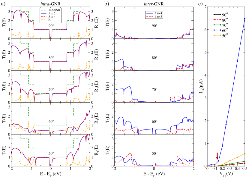
One important property observed for all considered rotation angles is the low reflection probability around the Fermi energy (see for instance the electrode 1 reflection function at Fig. 3a), indicating that in absence of external potential low energy electrons can propagate with negligible backscattering.
In Fig. 3c we present the calculated current flowing from electrode 1 to 4 as a function of an inter-GNR applied bias . The structure stands out when compared to all other cases, showing an inter-GNR current higher by one order of magnitude, in accordance with what one would expect from the zero bias transmission analysis. The red arrow at Fig. 3c indicates the onset of the inter-GNR current at meV (the non-zero values of bellow the onset observed for 60∘ are attributed to the small broadening used in the calculations).
At , the inter-GNR transport proves to be more than just a secondary effect. Rather it is as significant as the direct intra-GNR transport. Moreover, comparing the inter-GNR transmissions and (Fig. 3b), one can predict that the scattering states from electrode 1 that are transmitted to the crossing GNR will propagate most likely towards the electrode 4 rather than 3 for all , a remark that is most evident for .
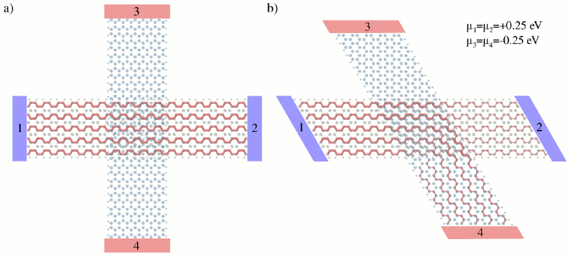
This prognosis is confirmed with the bond currents from electrode 1 calculated with an inter-GNR voltage of V (, with and ) and integrated over the energy window eV. On the one hand, with a setup (Fig. 4a), all scattering states from electrode 1 almost fully propagate towards terminal 2 and essentially no current flows to the crossing ribbon.222For a better visualization of the bond currents a cutoff was applied so that all bond currents below a given threshold are not printed. On the other hand, for (Fig. 4b) only about half of the states propagates towards terminal 2, while the other half is transmitted through the crossing to electrode 4, and no current flows from 1 to 3.
III.4 Operation of one GNR as a gate electrode
In this section we study the transport characteristics in the crossing as a function of inter- and intra-GNR voltages. The intra-GNR voltage was applied only among the electrodes 1 and 2, i.e., , while the electrodes 3 and 4 were maintained at the same chemical potential, . The inter-GNR voltage was defined by the difference between the chemical potentials from electrode 1 and 4, i.e., . Therefore, within this setup one can investigate how the GNR34 can act as a gate to the current flowing through GNR12 in crossing systems presenting low inter-GNR transmission, such as . Moreover, this allows one to tune the current splitting on devices with higher inter-GNR transmission, which is the case for .
In Fig. 5 we present the different components for the current with the variation of and , for both and devices. The intra-GNR current presents an onset at meV and is more sensitive for (top left panel in Fig. 5) where it clearly increases fast with but slower with , indicating that the GNR34 produces only a weak gating effect on the current flowing through GNR12. We note that this weak gating effect is in contrast with the calculations reported in Ref. Masum Habib and Lake, 2012, showing a current variation of several orders of magnitude with the inter-GNR bias. A possible reason for this discrepancy could be related to the nonequilibrium charge redistribution, an effect which we include in our present study. The inter-GNR current components , , and for 90∘ (left panels in Fig. 5) are all negligible compared to the intra-GNR , and essentially no change is observed within the applied bias range.
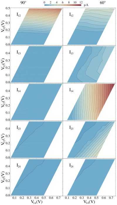
For the device (right panels in Fig. 5) the inter-GNR currents and present the same order of magnitude for . When a finite intra-GNR voltage is applied the main effect observed is that the current flowing to GNR34 arises more from electrode 1 and less from 2, meaning that the electron splitting can be tuned combining and .
III.5 Analysis of the scattering potential at the crossing
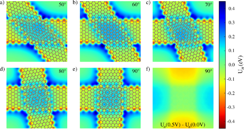
In order to characterize the change of the scattering properties in the crossing region, we present here results for the distribution of the electrostatic potential in the central region. This is defined as the Hartree potential plus the local pseudopotential describing the electron-ion interaction within the Siesta/TranSiesta packages Soler et al. (2002); Brandbyge et al. (2002); Papior et al. (2016). Fig. 6a-e show the electrostatic potential at the middle plane between the two ribbons resulting from our calculations at different angles and without applied voltage (). For all angles the potential is higher (more repulsive for electrons) in the crossing region, and with the highest values in regions where the lattices of the two ribbons match. This stems from the electron charge accumulation in the inter-ribbon region. Accordingly, for the case, where the lattices happen to match within the entire intersection region, the potential reveals “bumps” over the entire crossing, which might be interpreted as a source of larger scattering (and, thus, a harder barrier) for propagating electrons. Thus, one might be tempted to assign to this larger corrugation of the effective electron potential the simultaneous decrease of the intra-GNR and increase of the inter-GNR scattering at .
Fig. 6f explores whether this effect can be strongly modified at finite bias. In this figure we show the difference of the electrostatic potential for an inter-GNR voltage V (, with and ) and a zero bias () calculations for the device. This plot only reveals smooth changes in the self-consistent electrostatic potential due to the applied bias. In particular, we do not find noticiable changes in the crossing region. This indicates that the electron scattering at the crossing will not be drastically modified by the inter-GNR bias, in agreement with the general trends observed for the transmission functions presented so far.
III.6 Role of inter-ribbon distance
The above analysis of the electrostatic potential in the crossing suggests that the overlap of carbon -orbitals may produce a strong effect on the potential distribution and, thus, on the scattering at the crosssing, increasing the inter-GNR transmission. In order to test this hypothesis and to have a better understanding of the observed transport properties, we now consider the role of the inter-ribbon distance on the ratio between the intra- and inter-GNR transport.
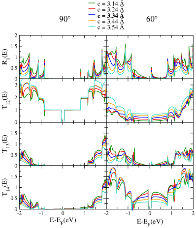
In Fig. 7 it is presented the electrode 1 zero bias reflection and transmissions as a function of the inter-ribbon distance around our reference value Å. We analyze two extreme cases, namely (the case with higher intra-GNR and lower inter-GNR transmissions) and (with lower intra-GNR and higher inter-GNR transmissions). Inside the varying interval of Å, almost no change is observed in the transmission for the 90∘ device close to . For higher energies, eV, the decreasing distance between the GNRs infers a stronger scattering effect, which is expressed in terms of the reflection probability . The dependence with the distance is significantly different for the 60∘ case (Fig. 7, on the right). As the distance between GNRs decreases we observe a clear increase of the inter-GNR transmission. This takes place at the expense of the intra-GNR transport, which gets drastically reduced. We note that this result indicates that the transmission in a device could be tuned by applying an external force to the junction. The feasibility of this kind of electromechanical switching has been also suggested for crossed carbon nanotubes. Yoon et al. (2001)
IV Discussion
IV.1 Lattice matching and registry index
To investigate the role of lattices matching in the crossing region, another set of calculations was performed by translating one GNR with respect to the other while keeping the inter-GNR distance at Å. In Fig. 8 the electrode 1 zero bias reflection and transmissions for structures with and are presented for the six different stacking configurations each. Very little difference is observed in the transmissions among the translated structures with 90∘ (left panels in Fig. 8). This is consistent with the idea of the overlap between the orbitals being the key parameter, since the average overlap does not vary much when translating the GNRs with . In other words, an average of the different stackings between carbon atoms in the two ribbons is always sampled when the ribbons cross at and, therefore, a small shift of the ribbons’ positions does not qualitatively change the situation.
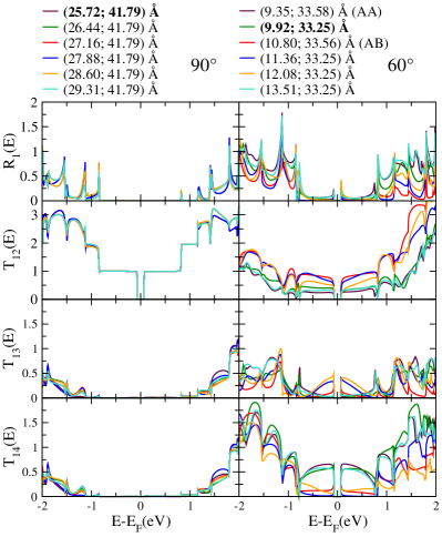
In contrast, for the 60∘ case the results show a strong change already close to (right panels in Fig. 8). Two particular stackings can be highlighted: AA (where the carbons from the different ribbons lay on top of each other in the crossing region) and AB (when half of the carbons lay on top of other carbons, while half of them resides on the center of the other GNR hexagons and, therefore, does not overlap). These two stacking correspond exactly to the maximum (AA) and minimum (AB) possible overlap between the carbon atoms in the crossing. Accordingly, the AA case presents the highest/lowest inter-/intra-GNR transmission, while for AB stacking one find the lowest/highest inter-/intra-GNR transmission.
So far, all results support the hypothesis that the overlap between -orbitals in the crossing determines the scattering properties in our system. However, if this simple picture would be enough to explain all the observed phenomena, one could in principle quantify the amount of scattering using some measure that characterizes the overlap for each structure. The registry index (RI) can be used to provide such a measure (see Hod (2013) for a detailed review). The idea is to consider a circle around each carbon atom belonging to the crossing region and compute the overlapping area between the circles from different GNRs. For graphene like materials it has been shown that the ideal circle radius to be considered corresponds to half of a C-C covalent bond length in graphene (i.e., 0.71 Å). The RI is then defined as , where and are respectively the maximum and minimum possible overlaps between the GNR orbitals.
Table 1 shows the RI calculated for structures with different intersection angles together with the special cases of with AA and AB stacking. Considering all the atoms in the crossing region (RItot), the highest value is obtained for with AA stacking (RI) and the minimum one for with AB stacking (RI), as one would expect from the definition above. This values qualitatively describes the changes of the inter-GNR currents among the 60∘ cases [A versus A]. Moreover, the calculated RItot exhibits a qualitative agreement with the transport properties for , , and devices. However, a discrepancy occurs when all cases are contemplated, since all devices with , including the AB stacking with RI, present higher inter-GNR current than all the other devices with different , for which RI.
| device | 60∘AA | 60∘AB | |||||
|---|---|---|---|---|---|---|---|
| RItot | 0.08 | 0.11 | 0.17 | 0.45 | 0.44 | 1.00 | 0.00 |
| RIedge | 0.00 | 0.24 | 0.35 | 0.12 | 0.55 | 1.00 | 0.15 |
One could consider that, for example, only the GNR edges in the crossing are relevant for describing the scattering properties. Hence the registry index can be calculated only considering the overlaps from carbons belonging to the GNR edges (RIedge). This will change the RI to quantitative different values, see Table 1. However, none of the registry index values does qualitatively describe the angle dependency on the current when all cases are taken into account.
IV.2 Simple model for inter-ribbon tunneling
The analysis in the previous section shows that the overlap of orbitals in the crossing region cannot alone account for the observed inter-GNR transmission and, in particular, explain what makes a device with a very interesting and effective candidate as a beam splitter.
The key to understand the physical origin of this important effect is to consider the tunneling probability between the relevant electronic states in each of the two crossing GNRs. To do this properly it is necessary to take into account not only the overlaps between atomic orbitals in neighboring structures, but also the relative phases and amplitudes with which these orbitals participate to those scattering states. The VB and CB states of the 14-AGNR calculated at the point with DFT are shown in Fig. 9a-b. These two states are representative for the available electron bands in the energy range of eV around . While the VB is characterized by an odd symmetry with respect to the GNR axis and the CB by an even symmetry, both states share a common structure with four nodal planes along the ribbon. Reminiscent of the electron states at the Dirac point in graphene,Castro Neto et al. (2009) these states reflect the characteristic ratio
| (6) |
between the electron momentum along the ribbon axis () and perpendicular to it (). The AGNR states can be interpreted as quantized states of a graphene layer and, thus, they can be qualitatively represented by a propagating wave along the ribbon axis with a Bloch wavevector together with a particle-in-a-box state corresponding to a wavevector in the confined (perpendicular) direction. Wakabayashi et al. (2010) Ignoring the details of the wavefunction inside the graphene unit cell, and just focusing on the envelope wavefunction, we just approximate this situation using plane-waves, in which case we are left with the traditional bands of a free-electron wire, i.e., we have
| (7) |
where depends on the GNR width and the quantum number (positive integer). The second AGNR is described similarly, but with rotated wavefunctions where the wavevectors in the two ribbons are related via the rotation matrix defined for a clockwise rotation angle :
| (8) | ||||
| (9) |
In an elastic scattering process the energy is conserved, i.e., the wavevectors generally fulfill the condition
| (10) |
As can be seen in Fig. 9c, the electronic structure obtained for the AGNRs using this simple particle-in-a-box quantization condition is qualitatively correct. In the spirit of perturbation theory, the inter-GNR tunneling probability Bardeen (1961); Masum Habib and Lake (2012); Van de Put et al. (2016) is assumed to be proportional to the modulus square of the overlap between the two wavefunctions,
| (11) |
These overlaps can readily be evaluated numerically as shown in Fig. 9d as a function of , , and the ratio . For the fundamental mode the two wavefunctions have a significant overlap in a large part of the parameter space. In the limit of (), where the two GNRs are aligned in parallel (antiparallel), the overlap goes to infinity because of the diverging integration area. As increases, the region with a significant overlap shrinks towards one universal curve. This situation corresponds to the wavevector matching condition 333Note that another matching condition is given by the relation , from where one obtains a maximum for , which taking into account the minus sign from corresponds to the same preferential scattering at 60∘.
| (12) |
which in turn yields the relationship
| (13) |
According to Eq. (6) this simply corresponds to , i.e., the exact condition for a maximal inter-GNR tunneling as found in our simulations for AGNR. The meaning of the condition Eq. (12) can be rephrased in very simple terms: for two ribbons interacting weakly and with a relatively large contact area (in units of the Fermi wavelength square) the tunneling probability will be maximized when the total wavevector of the electron is preserved in the elastic scattering process.
Notice that this simplified model cannot account for the dependence of the current on the stacking of the GNRs. In order to do so, in addition to the phases carried by the envelope wavefunctions it is necessary to account for the structure of the wavefunctions inside the graphene unit cell (and take into account for the overlaps between orbitals and their relative phases within the unit cell). This explains the partial success of the RI, that allows rationalizing the changes of the inter-GNR transport for a fixed angle . However, the main effect of the rotation angle is accounted for by our simplified model based on a description of the electronic states as plane waves.
Although Eq. (7) can be a good approximation for the CB and VB of AGNRs, the situation is more complicated for nanoribbons of different orientations and, in particular, for ZGNRs. Wakabayashi et al. (2009); Castro Neto et al. (2009); Wakabayashi et al. (2010); Lima et al. (2016) While qualitatively correct at intermediate energies, the quantized graphene bands fail to describe important features of the low energy spectrum of ZGNRs, as the appearance of the edge states at the Fermi level. Therefore, considering states sufficiently far from the Fermi energy, one can apply the simple model to ZGNRs, but in this case the relation between parallel and perpendicular momentum must be reversed,
| (14) |
Thus, for ZGNRs Eq. (13) gives rise to a maximum tunneling probability for , in agreement with the results reported in Ref. Lima et al., 2016 using a -orbital tight-biding model of the system.
Our results present clear connections with previous work investigating the modifications of bilayer graphene band structure as a function of the rotation angle of the two layers. Lopes dos Santos et al. (2007) The above argumentation explains why the alignment of the honeycomb lattices of the AGNR ribbons at intersection radically increases the inter-ribbon interaction regardless of stacking, why this also happens for ZGNRs, although there the electron scattering takes place preferentially at 120∘. It also explains the higher inter-GNR conductance at 30∘ and 90∘ reported in Ref. Botello-Méndez et al., 2011 for crossed AGNR/ZGNR devices.
V Conclusions
In this paper we studied the electronic and transport properties of a 4-terminal junction defined by two crossed 14-AGNRs from first-principles with the Siesta/TranSiesta codes Soler et al. (2002); Brandbyge et al. (2002); Papior et al. (2016). Our research comprises a detailed investigation of the system behavior under the variation of structural parameters, such as intersection angle, inter-GNR distance and stacking order, as well as its response under nonequilibrium conditions by considering different setups with a finite voltage applied between the electrodes.
Varying the intersection angle between the crossed AGNRs we found two extreme cases, namely and with low and high inter-GNR transmission, respectively. Remarkably, for the 60∘ case we found that the inter-GNR transmission channel is close to and the reflection negligible over a relatively large energy window of eV around the Fermi energy without an applied voltage. Moreover, for all considered cases with the majority of inter-transmitted electrons propagate only in one direction in the other ribbon. Those findings indicate that semiconducting crossed AGNR structures are interesting candidates to be incorporated in quantum electronics devices. In particular, we showed that a system with can operate as an electronic beam splitter where the ratio of intra/inter transmission can be tuned by changing the inter-GNR distance, i.e., it can be mechanically controlled by applying an external force to the junction.
We also explored how the crossed structures behave with biased electrodes. Applying an inter-GNR bias voltage, the 60∘ configuration is again distinguished with an inter-GNR current one order of magnitude higher than all the other considered intersection angles. When one AGNR is subjected to an intra-GNR bias voltage, changing the inter-GNR voltage produces a weak gating effect on the 90∘ devices, but reveals the possibility of tuning the current splitting on the 60∘ case.
Analyzing the electrostatic potential we found that the lattice matching on the crossing region plays an important role on the scattering properties. Indeed, a significant change on the transmission probabilities is observed by varying the stacking order on the 60∘ device. Those results suggest that the overlap of carbon orbitals is another essential parameter to the scattering process. The structures’ registry indices indicate that the amount of -orbital overlap in the crossing can qualitatively describe the changes in the inter-GNR currents among 60∘ cases as well as explain the trend in the transport properties for structures with . However, the registry index does not describe the inter-GNR transmission in a general fashion. To this extent we presented a simple model based on a description of the electronic states as plane waves that captures the effect of the angle. Furthermore, we show how our model explains the role of the intersection angle in crossed GNRs with different orientations.
The emerging picture from the combination of Ref. Lima et al. (2016) and the work presented here, is that GNRs with different chiralities and widths may be combined in nanoscale crossbar junctions which should allow, under suitable control of the intersection angle, to construct effective and tunable electronic beam splitters.
VI Acknowledgments
The authors acknowledge financial support from FP7 FET-ICT “Planar Atomic and Molecular Scale devices” (PAMS) project (funded by the European Commission under contract No. 610446), the Spanish Ministerio de Economia y Competitividad (MINECO) (Grant No. MAT2013-46593-C6-2-P), the Basque Dep. de Educación and the UPV/EHU (Grant No. IT-756-13).
References
- Bocquillon et al. (2014) E. Bocquillon, V. Freulon, F. D. Parmentier, J.-M. Berroir, B. Plaçais, C. Wahl, J. Rech, T. Jonckheere, T. Martin, C. Grenier, et al., “Electron quantum optics in ballistic chiral conductors,” Annalen Der Physik 526, 1 (2014).
- Henny et al. (1999) M. Henny, S. Oberholzer, C. Strunk, T. Heinzel, K. Ensslin, M. Holland, and C. Schönenberger, “The Fermionic Hanbury Brown and Twiss experiment,” Science 284, 296 (1999).
- Oliver et al. (1999) W. D. Oliver, J. Kim, R. C. Liu, and Y. Yamamoto, “Hanbury Brown and Twiss-type experiment with electrons,” Science 284, 299 (1999).
- Samuelsson et al. (2004) P. Samuelsson, E. V. Sukhorukov, and M. Büttiker, “Two-particle Aharonov–Bohm effect and entanglement in the electronic Hanbury Brown–Twiss setup,” Phys. Rev. Lett. 92, 026805 (2004).
- Neder et al. (2007) I. Neder, N. Ofek, Y. Chung, M. Heiblum, D. Mahalu, and V. Umansky, “Interference between two indistinguishable electrons from independent sources,” Nature 448, 333 (2007).
- Splettstoesser et al. (2010) J. Splettstoesser, P. Samuelsson, M. Moskalets, and M. Büttiker, “Two-particle Aharonov–Bohm effect in electronic interferometers,” J. Phys. A: Math. Theor. 43, 354027 (2010).
- Ji et al. (2003) Y. Ji, Y. Chung, D. Sprinzak, M. Heiblum, D. Mahalu, and H. Shtrikman, “An electronic Mach–Zehnder interferometer,” Nature 422, 415 (2003).
- Roulleau et al. (2007) P. Roulleau, F. Portier, D. C. Glattli, P. Roche, A. Cavanna, G. Faini, U. Gennser, and D. Mailly, “Finite bias visibility of the electronic Mach-Zehnder interferometer,” Phys. Rev. B 76, 161309 (2007).
- Fève et al. (2007) G. Fève, A. Mahé, J.-M. Berroir, T. Kontos, B. Plaçais, D. C. Glattli, A. Cavanna, B. Etienne, and Y. Jin, “An on-demand coherent single-electron source,” Science 316, 1169 (2007).
- Dubois et al. (2013) J. Dubois, T. Jullien, F. Portier, P. Roche, A. Cavanna, Y. Jin, W. Wegscheider, P. Roulleau, and D. C. Glattli, “Minimal-excitation states for electron quantum optics using levitons,” Nature 502, 659 (2013).
- Bocquillon et al. (2013) E. Bocquillon, V. Freulon, J.-M. Berroir, P. Degiovanni, B. Plaçais, A. Cavanna, Y. Jin, and G. Fève, “Coherence and indistinguishability of single electrons emitted by independent sources,” Science 339, 1054 (2013).
- Waldie et al. (2015) J. Waldie, P. See, V. Kashcheyevs, J. P. Griffiths, I. Farrer, G. A. C. Jones, D. A. Ritchie, T. J. B. M. Janssen, and M. Kataoka, “Measurement and control of electron wave packets from a single-electron source,” Phys. Rev. B 92, 125305 (2015).
- Ryu et al. (2016) S. Ryu, M. Kataoka, and H.-S. Sim, “Ultrafast Emission and Detection of a Single-Electron Gaussian Wave Packet: A Theoretical Study,” Phys. Rev. Lett. 117, 146802 (2016).
- Hofstetter et al. (2009) L. Hofstetter, S. Csonka, J. Nygård, and C. Schönenberger, “Cooper pair splitter realized in a two-quantum-dot Y-junction,” Nature 461, 960 (2009).
- Ubbelohde et al. (2014) N. Ubbelohde, F. Hohls, V. Kashcheyevs, T. Wagner, L. Fricke, B. Kästner, K. Pierz, H. W. Schumacher, and R. J. Haug, “Partitioning of on-demand electron pairs,” Nat. Nanotechnol. 10, 46 (2014).
- Fujita et al. (1996) M. Fujita, K. Wakabayashi, K. Nakada, and K. Kusakabe, “Peculiar localized state at zigzag graphite edge,” J. Phys. Soc. Jpn. 65, 1920 (1996).
- Nakada et al. (1996) K. Nakada, M. Fujita, G. Dresselhaus, and M. S. Dresselhaus, “Edge state in graphene ribbons: Nanometer size effect and edge shape dependence,” Phys. Rev. B 54, 17954 (1996).
- Wakabayashi et al. (1999) K. Wakabayashi, M. Fujita, H. Ajiki, and M. Sigrist, “Electronic and magnetic properties of nanographite ribbons,” Phys. Rev. B 59, 8271 (1999).
- Han et al. (2007) M. Y. Han, B. Özyilmaz, Y. Zhang, and P. Kim, “Energy band-gap engineering of graphene nanoribbons,” Phys. Rev. Lett. 98, 206805 (2007).
- Son et al. (2006) Y.-W. Son, M. L. Cohen, and S. G. Louie, “Energy gaps in graphene nanoribbons,” Phys. Rev. Lett. 97, 216803 (2006).
- Yang et al. (2007) L. Yang, C.-H. Park, Y.-W. Son, M. L. Cohen, and S. G. Louie, “Quasiparticle energies and band gaps in graphene nanoribbons,” Phys. Rev. Lett. 99, 186801 (2007).
- Cai et al. (2010) J. Cai, P. Ruffieux, R. Jaafar, M. Bieri, T. Braun, S. Blankenburg, M. Muoth, A. P. Seitsonen, M. Saleh, X. Feng, et al., “Atomically precise bottom-up fabrication of graphene nanoribbons,” Nature 466, 470 (2010).
- Ruffieux et al. (2016) P. Ruffieux, S. Wang, B. Yang, C. Sánchez-Sánchez, J. Liu, T. Dienel, L. Talirz, P. Shinde, C. A. Pignedoli, D. Passerone, et al., “On-surface synthesis of graphene nanoribbons with zigzag edge topology,” Nature 531, 489 (2016).
- Oliveira et al. (2015) M. H. Oliveira, Jr., J. M. J. Lopes, T. Schumann, L. A. Galves, M. Ramsteiner, K. Berlin, A. Trampert, and H. Riechert, “Synthesis of quasi-free-standing bilayer graphene nanoribbons on sic surfaces,” Nat. Commun. 6, 7632 (2015).
- Jacobberger et al. (2015) R. M. Jacobberger, B. Kiraly, M. Fortin-Deschenes, P. L. Levesque, K. M. McElhinny, G. J. Brady, R. Rojas Delgado, S. Singha Roy, A. Mannix, M. G. Lagally, et al., “Direct oriented growth of armchair graphene nanoribbons on germanium,” Nat. Commun. 6, 8006 (2015).
- Koch et al. (2012) M. Koch, F. Ample, C. Joachim, and L. Grill, “Voltage-dependent conductance of a single graphene nanoribbon,” Nature Nanotechnol. 7, 713 (2012).
- Kawai et al. (2016) S. Kawai, A. Benassi, E. Gnecco, H. Söde, R. Pawlak, X. Feng, K. Müllen, D. Passerone, C. A. Pignedoli, P. Ruffieux, et al., “Superlubricity of graphene nanoribbons on gold surfaces,” Science 351, 957 (2016).
- Fuhrer et al. (2000) M. S. Fuhrer, J. Nygård, L. Shih, M. Forero, Y.-G. Yoon, M. S. C. Mazzoni, H. J. Choi, J. Ihm, S. G. Louie, A. Zettl, et al., “Crossed nanotube junctions,” Science 288, 494 (2000).
- Yoon et al. (2001) Y.-G. Yoon, M. S. C. Mazzoni, H. J. Choi, J. Ihm, and S. G. Louie, “Structural deformation and intertube conductance of crossed carbon nanotube junctions,” Phys. Rev. Lett. 86, 688 (2001).
- Jiao et al. (2010) L. Jiao, L. Zhang, L. Ding, J. Liu, and H. Dai, “Aligned graphene nanoribbons and crossbars from unzipped carbon nanotubes,” Nano Research 3, 387 (2010).
- Lima et al. (2016) L. R. F. Lima, A. R. Hernández, F. A. Pinheiro, and C. Lewenkopf, “A 50/50 electronic beam splitter in graphene nanoribbons as a building block for electron optics,” J. Phys.: Condens. Matter 28, 505303 (2016).
- López-Bezanilla et al. (2009) A. López-Bezanilla, F. Triozon, and S. Roche, “Chemical functionalization effects on armchair graphene nanoribbon transport,” Nano Lett. 9, 2537 (2009).
- Osella et al. (2012) S. Osella, A. Narita, M. G. Schwab, Y. Hernandez, X. Feng, K. Müllen, and D. Beljonne, “Graphene nanoribbons as low band gap donor materials for organic photovoltaics: Quantum chemical aided design,” ACS Nano 6, 5539 (2012).
- Villegas et al. (2014) C. E. P. Villegas, P. B. Mendonça, and A. R. Rocha, “Optical spectrum of bottom-up graphene nanoribbons: towards efficient atom-thick excitonic solar cells,” Sci. Rep. 4, 6579 (2014).
- Tan et al. (2011) Z. W. Tan, J.-S. Wang, and C. K. Gan, “First-principles study of heat transport properties of graphene nanoribbons,” Nano Lett. 11, 214 (2011).
- Saha et al. (2011) K. K. Saha, T. Markussen, K. S. Thygesen, and B. K. Nikolić, “Multiterminal single-molecule-graphene-nanoribbon junctions with the thermoelectric figure of merit optimized via evanescent mode transport and gate voltage,” Phys. Rev. B 84, 041412 (2011).
- Sevincli et al. (2013) H. Sevincli, C. Sevik, T. Cagin, and G. Cuniberti, “A bottom-up route to enhance thermoelectric figures of merit in graphene nanoribbons,” Sci. Rep. 3, 1228 (2013).
- Wilhelm et al. (2014) J. Wilhelm, M. Walz, and F. Evers, “Ab initio quantum transport through armchair graphene nanoribbons: Streamlines in the current density,” Phys. Rev. B 89, 195406 (2014).
- Christensen et al. (2015) R. B. Christensen, T. Frederiksen, and M. Brandbyge, “Identification of pristine and defective graphene nanoribbons by phonon signatures in the electron transport characteristics,” Phys. Rev. B 91, 075434 (2015).
- Kim and Kim (2008) W. Y. Kim and K. S. Kim, “Prediction of very large values of magnetoresistance in a graphene nanoribbon device,” Nat. Nano. 3, 408 (2008).
- Zeng et al. (2010) M. G. Zeng, L. Shen, Y. Q. Cai, Z. D. Sha, and Y. P. Feng, “Perfect spin-filter and spin-valve in carbon atomic chains,” Appl. Phys. Lett. 96, 042104 (2010).
- Zeng et al. (2011) M. Zeng, L. Shen, M. Zhou, C. Zhang, and Y. Feng, “Graphene-based bipolar spin diode and spin transistor: Rectification and amplification of spin-polarized current,” Phys. Rev. B 83, 115427 (2011).
- Soriano et al. (2010) D. Soriano, F. Muñoz Rojas, J. Fernández-Rossier, and J. J. Palacios, “Hydrogenated graphene nanoribbons for spintronics,” Phys. Rev. B 81, 165409 (2010).
- Wilhelm et al. (2015) J. Wilhelm, M. Walz, and F. Evers, “Ab initio spin-flip conductance of hydrogenated graphene nanoribbons: Spin-orbit interaction and scattering with local impurity spins,” Phys. Rev. B 92, 014405 (2015).
- Jayasekera and Mintmire (2007) T. Jayasekera and J. W. Mintmire, “Transport in multiterminal graphene nanodevices,” Nanotechnology 18, 424033 (2007).
- Areshkin and White (2007) D. A. Areshkin and C. T. White, “Building blocks for integrated graphene circuits,” Nano Lett. 7, 3253 (2007).
- Botello-Méndez et al. (2011) A. R. Botello-Méndez, E. Cruz-Silva, J. M. Romo-Herrera, F. López-Urías, M. Terrones, B. G. Sumpter, H. Terrones, J.-C. Charlier, and V. Meunier, “Quantum transport in graphene nanonetworks,” Nano Lett. 11, 3058 (2011).
- Xu et al. (2013) J. G. Xu, L. Wang, and M. Q. Weng, “Quasi-bound states and fano effect in t-shaped graphene nanoribbons,” J. Appl. Phys. 114, 153701 (2013).
- Masum Habib and Lake (2012) K. M. Masum Habib and R. K. Lake, “Current modulation by voltage control of the quantum phase in crossed graphene nanoribbons,” Phys. Rev. B 86, 045418 (2012).
- Masum Habib et al. (2013) K. M. Masum Habib, F. Zahid, and R. K. Lake, “Multi-state current switching by voltage controlled coupling of crossed graphene nanoribbons,” J. Appl. Phys. 114, 153710 (2013).
- Saha and Nikolic (2013) K. K. Saha and B. K. Nikolic, “Negative differential resistance in graphene-nanoribbon-carbon-nanotube crossbars: a first-principles multiterminal quantum transport study,” J. Comput. Electron. 12, 542 (2013).
- Van de Put et al. (2016) M. L. Van de Put, W. G. Vandenberghe, B. Sorée, W. Magnus, and M. V. Fischetti, “Inter-ribbon tunneling in graphene: An atomistic Bardeen approach,” J. Appl. Phys. 119, 214306 (2016).
- Saha et al. (2009) K. K. Saha, W. Lu, J. Bernholc, and V. Meunier, “First-principles methodology for quantum transport in multiterminal junctions,” J. Chem. Phys. 131, 164105 (2009).
- Ferrer et al. (2014) J. Ferrer, C. J. Lambert, V. M. García-Suárez, D. Z. Manrique, D. Visontai, L. Oroszlany, R. Rodríguez-Ferradás, I. Grace, S. W. D. Bailey, K. Gillemot, et al., “Gollum: a next-generation simulation tool for electron, thermal and spin transport,” New J. Phys. 16, 093029 (2014).
- Brandbyge et al. (2002) M. Brandbyge, J.-L. Mozos, P. Ordejón, J. Taylor, and K. Stokbro, “Density-functional method for nonequilibrium electron transport,” Phys. Rev. B 65, 165401 (2002).
- Papior et al. (2016) N. Papior, N. Lorente, T. Frederiksen, A. García, and M. Brandbyge, “Improvements on non-equilibrium and transport Green function techniques: the next-generation TranSIESTA,” Comp. Phys. Comm. p. in press (2016).
- Soler et al. (2002) J. M. Soler, E. Artacho, J. D. Gale, A. García, J. Junquera, P. Ordejón, and D. Sánchez-Portal, “The siesta method for ab initio order-n materials simulation,” J. Phys.: Condens. Matter 14, 2745 (2002).
- Keldysh (1965) L. V. Keldysh, “Diagram technique for nonequilibrium processes,” Sov. Phys. JETP-USSR 20, 1018 (1965).
- Kadanoff and Baym (1962) L. P. Kadanoff and G. Baym, Quantum Statistical Mechanics: Green’s Function Methods in Equilibrium and Nonequilibrium Problems (W. A. Benjamin, 1962), ISBN 9780201094220.
- Büttiker (1986) M. Büttiker, “Four-terminal phase-coherent conductance,” Phys. Rev. Lett. 57, 1761 (1986).
- Todorov (2002) T. Todorov, “Tight-binding simulation of current-carrying nanostructures,” J. Phys: Condens. Matter 14, 3049 (2002).
- Dion et al. (2004) M. Dion, H. Rydberg, E. Schröder, D. C. Langreth, and B. I. Lundqvist, “Van der Waals density functional for general geometries,” Phys. Rev. Lett. 92, 246401 (2004).
- Klimeš et al. (2010) J. Klimeš, D. R. Bowler, and A. Michaelides, “Chemical accuracy for the van der Waals density functional,” J. Phys.: Condens. Matter 22, 022201 (2010).
- Santos et al. (2012) H. Santos, A. Ayuela, L. Chico, and E. Artacho, “van der Waals interaction in magnetic bilayer graphene nanoribbons,” Phys. Rev. B 85, 245430 (2012).
- Troullier and Martins (1991) N. Troullier and J. L. Martins, “Efficient pseudopotentials for plane-wave calculations,” Phys. Rev. B 43, 1993 (1991).
- Note (1) Note1, using the same functional and basis set, we found that for bilayer graphene the equilibrium distance between the two layers is 3.486 Å for an AA stacking and 3.294 Å for AB stacking. For a crossed GNR system with one GNR rotated by 90∘ with respect to the other, we found 3.339 Å as the lowest energy distance, which lies in between these two extremes values for a bilayer graphene. Moreover, the lattice parameter calculated for graphite with different stackings ( Å, Å and Å), which are in close agreement with experiment measurements of Å Baskin and Meyer (1955); Zhao and Spain (1989), also presents an interlayer distance between the bilayer graphene values for AA and AB stacking. Therefore, we found reasonable to use the distance Å as the reference value for all our crossed structures.
- Note (2) Note2, for a better visualization of the bond currents a cutoff was applied so that all bond currents below a given threshold are not printed.
- Hod (2013) O. Hod, “The registry index: A quantitative measure of materials′ interfacial commensurability,” Chem. Phys. Chem. 14, 2376 (2013).
- Castro Neto et al. (2009) A. H. Castro Neto, F. Guinea, N. M. R. Peres, K. S. Novoselov, and A. K. Geim, “The electronic properties of graphene,” Rev. Mod. Phys. 81, 109 (2009).
- Wakabayashi et al. (2010) K. Wakabayashi, K. ichi Sasaki, T. Nakanishi, and T. Enoki, “Electronic states of graphene nanoribbons and analytical solutions,” Sci. Technol. Adv. Mater. 11, 054504 (2010).
- Bardeen (1961) J. Bardeen, “Tunnelling from a many-particle point of view,” Phys. Rev. Lett. 6, 57 (1961).
- Note (3) Note3, note that another matching condition is given by the relation , from where one obtains a maximum for , which taking into account the minus sign from corresponds to the same preferential scattering at 60∘.
- Wakabayashi et al. (2009) K. Wakabayashi, Y. Takane, M. Yamamoto, and M. Sigrist, “Edge effect on electronic transport properties of graphene nanoribbons and presence of perfectly conducting channel,” Carbon 47, 124 (2009).
- Lopes dos Santos et al. (2007) J. M. B. Lopes dos Santos, N. M. R. Peres, and A. H. Castro Neto, “Graphene bilayer with a twist: Electronic structure,” Phys. Rev. Lett. 99, 256802 (2007).
- Baskin and Meyer (1955) Y. Baskin and L. Meyer, “Lattice constants of graphite at low temperatures,” Phys. Rev. 100, 544 (1955).
- Zhao and Spain (1989) Y. X. Zhao and I. L. Spain, “X-ray diffraction data for graphite to 20 gpa,” Phys. Rev. B 40, 993 (1989).