One-dimensional electron gas in strained lateral heterostructures of single layer materials
Abstract
Confinement of the electron gas along one of the spatial directions opens an avenue for studying fundamentals of quantum transport along the side of numerous practical electronic applications, with high-electron-mobility transistors being a prominent example. A heterojunction of two materials with dissimilar electronic polarisation can be used for engineering of the conducting channel. Extension of this concept to single-layer materials leads to one-dimensional electron gas (1DEG). \ceMoS2/\ceWS2 lateral heterostructure is used as a prototype for the realisation of 1DEG. The electronic polarisation discontinuity is achieved by straining the heterojunction taking advantage of dissimilarities in the piezoelectric coupling between \ceMoS2 and \ceWS2. A complete theory that describes an induced electric field profile in lateral heterojunctions of two-dimensional materials is proposed and verified by first principle calculations.
pacs:
TBDConfinement of electrons along one of the spatial directions results in a two-dimensional electron gas (2DEG) that exhibits interesting physical phenomena along the side of useful technological applications. Particular examples include the field of quantum transport and mesoscopic physics Klitzing_PRL_45_1980 as well as high-electron-mobility transistors that are used in integrated circuits as digital on-off switches Dimitrijev_MB_40_2015 . The advantage of 2DEG conducting channel is the high mobility of charge carriers due to the absence of deleterious effects inherent to ionised impurity scattering that allows for ballistic transport Kumar_PRL_105_2010 . Engineering of 2DEG conventionally requires the use of a modulation doping technique Dingle_APL_33_1978 as in the case of (AlGa)As/GaAs heterostructures. Alternatively, the 2DEG can be achieved in undoped structures with an extreme band bending induced by the strong electric field at a heterojunction between two dielectric materials with dissimilar electronic polarisation such as (AlGa)N/GaN interface Khan_APL_60_1992 ; Ambacher_JAP_87_2000 . It is interesting to see whether polarisation effects in two-dimensional (2D) materials can be used to achieve confinements of electrons along one spatial direction?
2D materials become a perspective avenue for keeping up with latest trends in miniaturisation of electronics, culminating in a demonstration of the single layer \ceMoS2 transistor Radisavljevic_NN_6_2011 ; Kim_NC_3_2012 ; Radisavljevic_NM_12_2013 . Unlike group III-nitrides, free-standing transition-metal dichalcogenides do not possess spontaneous polarisation due to symmetry arguments. However, single-atomic-layer h-BN and monolayer transition-metal dichalcogenides have been theoretically predicted Duerloo_JPCL_3_2012 and experimental confirmed Wu_N_514_2014 ; Zhu_NN_10_2015 to show piezoelectricity as a result of strain-induced lattice distortions. Two types of heterostructures that involve 2D materials are discussed in the literature: (i) multilayer heterostructures produced by stacking of different 2D materials, so-called van der Waals heterostructures Geim_N_499_2013 , and (ii) lateral heterostructures, which are formed when two materials are covalently bonded within the 2D plane Huang_NM_13_2014 .
It will be shown that a lateral heterojunction of 2D materials with dissimilar piezoelectric properties can be used to achieve additional confinement of charge carriers along the interface, which creates conditions for realisation of a one-dimensional electron gas (1DEG). A complete theory that describes an induced electric field profile in lateral heterojunctions of 2D materials is presented and verified by first principle calculations.
First-principle model
First, we will use an ab initio model to explore the feasibility of achieving conditions for 1D confinement of charge carriers in a lateral heterojunction of two single-layer materials. For this purpose, an 80-atoms \ceMoS2/\ceWS2 supercell is constructed as illustrated in Fig. 1(a). \ceMoS2 and \ceWS2 are chosen due to an almost identical lattice parameter of two materials (less that 0.1% mismatch), which reduces the misfit strain at the interface. One would expect the heterostructure to possess no built-in electric field since transition metal dichalcogenides manifest no net polarisation unlike group-III nitride bulk semiconductors. This hypothesis can be verified by plotting the potential energy across the heterojunction (Fig. 1, b). The potential energy profile shows periodic oscillations with minima in the vicinity of nuclei and maxima corresponding to interstitial regions. It is evident that maxima of the potential energy remain constant within \ceMoS2 and \ceWS2 domains with an abrupt step-like transition at the interface. The confinement of charge carriers resembles that in a quantum well (Fig. 1,d).
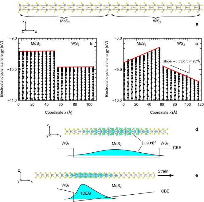
Next, the same heterostructure is uniformly strained in the direction perpendicular to the heterojunction, i.e., along -axis (Fig. 1, a). The magnitude of strain is deliberately chosen high (10%) in order to magnify observed effects. The Poisson’s contraction is simulated by relaxing the second lateral dimension of the supercell to eliminate the macroscopic stress , accompanied by a full relaxation of internal degrees of freedom. It is found that, after relaxation, the macroscopic strain of 10% is non-uniformly distributed among both material domains. The effective strain in \ceMoS2 is 10.5%, while \ceWS2 accommodates only 9.5%. This result can be attributed to differences in stiffness between two materials.
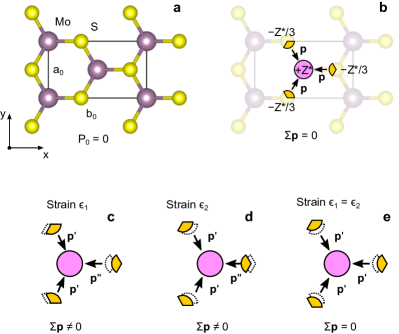
It is also noticed that the external strain breaks 3-fold rotational symmetry, which is responsible for the absence of spontaneous polarisation in \ceMoS2 and \ceWS2 due to the cancellation of polarisation dipoles (Fig. 2). The symmetry breaking is evident from the disparity in Mo-S bond lengths: 2.52 Å vs 2.41 Å for the bonds oriented along or tilted with respect to the strain direction. The electrostatic potential profile plotted in Fig. 1(c) reveals the presence of an electric field in \ceMoS2 and \ceWS2 domains of approximately equal magnitude, but the opposite direction. The magnitude of electric field varies (%) depending on the coordinates of the line scan (see Supplementary information for more details); the average field is approximately mV/Å. The created saw-like potential confines charge carriers in the vicinity of the \ceMoS2/\ceWS2 interface (Fig. 1,e) producing a narrow 1D conduction channel along -axis of the width a few interatomic spacings.
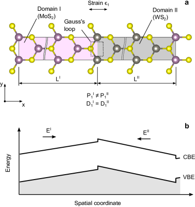
Qualitatively, an origin of the electric field can be attributed to heterogeneity in polarisation induced by the strain in \ceMoS2 and \ceWS2 domains (see Fig. 3). To gain a quantitative understanding of the observed effects in 2D materials, a model that couples continuum mechanics and Poisson equation is developed below.
Continuum model
The purpose of this model is to describe the electric field profile induced due to piezoelectric effects in 2D strained heterostructures. The problem is similar to that solved by Ambacher et al. Ambacher_JAP_87_2000 for AlGaN/GaN heterostructures, however, there are peculiarities related to 2D character of the materials in question, which warrant repeating some basic steps.
The free electro-elastic energy density stored in a linear medium can be expressed as meitzler1988ieee
| (1) |
where are components of the strain tensor written in the Voigt’s matrix notations, is the electric field projection along axis, are components of the stiffness matrix, are components of the electrical permittivity tensor of the material, and the range of indices , is adapted to 2D. Oftentimes, the macroscopic strain is found by minimising the elastic energy only Ambacher_JAP_87_2000 (first term in Eq. (1)). However, it should be emphasised that the electric field and strain are coupled through the electric displacement, which takes the form
| (2) |
Here is the permanent (spontaneous) polarisation and are components of piezoelectric strain tensor. In the absence of free charges, the Gauss’s law requires
| (3) |
This implies continuity of the electric displacement at the interface of two domains (see Fig. 3,a)
| (4) |
which includes contributions from permanent, strain-induced, and field-induced electric dipoles in the material. The strain and electric field distributions can be found by minimising the total electro-elastic energy
| (5) |
subject to boundary conditions, e.g., an applied macroscopic strain.
2D materials pose a challenge related to defining the integration volume required to evaluate the total free energy in Eq. (5). There are attempts in the literature Huang_PRB_74_2006 to assign an effective thickness to atomically thin monolayers to compare their properties (strength, elastic modulus, or dielectric constant) to bulk materials. However, such analysis always bares the element of ambiguity. Alternatively, it seems more logical for 2D materials to use area rather than volume for normalising their specific properties. As a result, the stiffness coefficients acquire units of N/m, whereas the piezoelectric coefficients are expressed in units of C/m in 2D Duerloo_JPCL_3_2012 . To remain consistent, an effective 2D dielectric permittivity needs to be defined. Then Eqs. (1)–(5) can be readily extended to 2D materials, provided the free energy in Eq. (5) is integrated over the surface area, which eliminates ambiguities associated with the layer thickness.
| \ceMoS2 | \ceWS2 | ||||
|---|---|---|---|---|---|
| Parameter | Units | Calculated | Other sources | Calculated | Other sources |
| Å | 3.185 | 3.16111Experimental Wilson_AP_18_1969 , 3.19222Calculated with DFT/GGA Duerloo_JPCL_3_2012 | 3.188 | 3.15, 3.19 | |
| N/m | 133 | 130 | 146 | 144 | |
| N/m | 33 | 32 | 32 | 31 | |
| pC/m | 359 | 333Experimental Zhu_NN_10_2015 , 364 | 249 | 247 | |
| F | 444Obtained using Eq. (6) based on \ceMoS2 bulk in-plane relative dielectric permittivity of 15 and the interlayer separation of 6.02 Å Liang_N_6_2014 . | 555Obtained using Eq. (6) based on \ceWS2 bulk in-plane relative dielectric permittivity of 14 and the interlayer separation of 6.06 Å Liang_N_6_2014 . | |||
Structural, elastic, piezoelectric, and dielectric properties of monolayer \ceMoS2 and \ceWS2 are gathered in Table 1. The structural unit and orientation of coordinate axes are illustrated in Fig. 2(a). The calculated lattice parameters are in agreement with experiment and other calculations reported in the literature. The hexagonal symmetry of a single layer (point group D) reduces the number of independent coefficients in the stiffness matrix down to two: and NyeJ_1985_Physical_prop_crystals . Our values of and listed in Table 1 agree with those obtained in previous DFT calculations. The piezoelectric tensor is characterised by a single independent element , due to symmetry arguments. The calculated values agree well with prior theoretical studies. However, approximately 20% deviation from existing experimental data is observed. This deviation is acceptable giving the large uncertainty of experimental measurements.
The static dielectric permittivity is one of the least studied properties of single-layer transition metal dichalcogenides. The present calculations yield the value of for the in-plane relative dielectric permittivity of a single-layer \ceMoS2, with being the permittivity of free space. It should be emphasised that is an extensive property, which is determined by the thickness of the vacuum layer that is used for separation between periodical images in the direction perpendicular to the planar structure. To represent a free-standing layer of \ceMoS2, the value of Å was chosen, which is approximately by a factor of four greater than the spacing between layers in bulk. Berkelbach et al. Berkelbach_PRB_88_2013 proposed evaluation of the effective 2D polarizability of planar materials using the following relationship
| (6) |
which yields the effective in-plane polarizability of F, as compared to the value of F obtained for bulk \ceMoS2 (see Table 1).
Potential energy profile scans similar to those shown Fig. 1 reveal the presence of a zig-zag electric field even in the middle of the vacuum region due to periodic boundary conditions along -axis (see Supplementary information). To capture the energy stored in the vacuum due to the finite electric field, the effective 2D dielectric permittivity used in calculation of the free energy density in Eq. (1) is expressed as
| (7) |
The additional term contributes approximately 25% to the value of .
Minimization of the total free energy for the 2D strained lateral heterostructure of \ceMoS2 and \ceWS2 was performed using a Lagrange multiplier approach with respect to the strain tensor and electric field in both domains (see Methods for details). The quasi-2D continuum model with material parameters listed in Table 1 yields the strain distribution of and , which is in excellent agreement with DFT results. The greater strain in \ceMoS2 (domain I) is due to its lower stiffness as compared to \ceWS2 (see Table 1). The continuum model also properly captures magnitude of the electric field V/m, which coincides with the average slope of the electrostatic potential profile obtained from first-principle calculations.
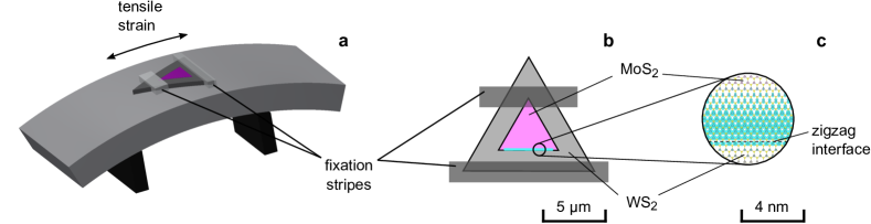
Finally, we would like to comment on a practical realisation of the strained heterostructures discussed in this paper. \ceMoS2/\ceWS2 lateral heterostructures usually have a morphology of equilateral triangular flakes of the size of a few micrometres Gong_NM_13_2014 ; Huang_NM_13_2014 . \ceMoS2 forms an inner core surrounded by the \ceWS2 outer layer Bogaert_NL_16_2016 . Gong et al.Gong_NM_13_2014 reported achieving an atomically sharp \ceMoS2/\ceWS2 in-plane interface. The interface is preferentially formed along “zigzag” direction (the y-axis in Fig. 3,a), which is consistent with the structural model studied here. The strain can be applied employing a setup shown in Fig. 4 previously used by Conley et al.Conley_NL_13_2013 to measure the band gap shift of \ceMoS2 with strain. The method involves clamping of a specimen at the surface of a mechanically bent substrate, which allows applying of a uniform strain up to 2% in a highly controlled manner. The strain magnitude much less than 10% can be sufficient giving a much larger length of real heterostructures in comparison to that modelled here. The presence of a strain-induced electric field can be verified by measuring a photoluminescence (PL). In unstrained \ceMoS2/\ceWS2 lateral heterostructures, the PL intensity is enhanced at the \ceMoS2/\ceWS2 interface Gong_NM_13_2014 ; Huang_NM_13_2014 due to the type-II band alignment Kang_JPCC_119_2015 . The PL intensity at the interface that develops 1DEG is expected to diminish when the strain is applied due to the induced electric field that separates charge carriers.
Conclusions
One-dimensional conductivity channel is obtained in a lateral \ceMoS2/\ceWS2 heterojunction. Conducting electronic states are confined along the interface by an inhomogeneous electric field that is induced by differences in the piezoelectric and elastic response of two materials thereby creating a one-dimensional electron gas. An effective model that captures interactions between electric and elastic degrees of freedom in low-dimensional heterostructures is developed. The model accurately predicts the magnitude of macroscopic electric field induced in the strained heterostructure as verified by ab initio calculations. This realisation of 1D electron gas creates an alternative to a quasi 1D conducting channel formed in the 2D electron gas of GaAs/(AlGa)As heterostructures by electrostatic gating Thornton_PRL_56_1986 ; Berggren_PTRSA_368_2010 that can be potentially used for low-power switching applications.
Methods
Calculation of structural, elastic, and dielectric properties. Electronic structure calculations of single-layer hexagonal \ceMoS2 and \ceWS2 have been performed in the framework of the density functional theory (DFT) Kohn_PR_140_1965 using Perdew-Burke-Ernzerhof generalized gradient approximation (GGA-PBE) for the exchange-correlation functional Perdew_PRL_77_1996 . Structural, elastic, and dielectric properties were modelled using the Vienna ab initio simulation program (VASP) and projector augmented-wave (PAW) potentials Kresse_PRB_54_1996 ; Kresse_PRB_59_1999 ; Blochl_PRB_50_1994 . The structure was represented by a single layer of \ceMoS2 or \ceWS2 with a vacuum separation, which is approximately equal to a quadruple value of the equilibrium spacing between layers of the bulk 2H-\ceMoS2. The structural optimisation was carried out in conjunction with relaxation of the in-plane lattice parameter . The structure was considered optimised when the magnitude of Hellmann-Feynman forces acting on atoms dropped below 2 meV/Å. The Brillouin zone of the primitive unit cell was sampled using Monkhorst-Pack grid Monkhorst_PRB_13_1976 . The mesh was appropriately scaled when supercells are considered.
A hard PAW potential was used to represent sulphur (S_h). Semi-core electrons were included as valence electrons in molybdenum (Mo_sv) and tungsten (W_pv). The cutoff energy for a plane wave expansion was set at 500 eV, which is 25% higher than the value recommended in the pseudopotential file. The higher cutoff energy was essential for obtaining accurate, converged lattice parameters.
The elastic tensor was determined using a finite differences technique from the strain-stress relationship calculated in response to finite distortions of the lattice taking into account relaxation of the ions. The total of eight strained structures that represent various permutations of the strain were considered.
The relaxed-ion dielectric tensor was calculated using the finite external electric field of the magnitude 1 meV/Å. The tight energy convergence of eV was required to achieve the accuracy of 0.1 for the relative dielectric permittivity.
Calculation of piezoelectric coefficients. Calculations of piezoelectric coefficients were performed using a full potential linear augmented plane wave method implemented in Wien2k package Blaha_2001 in conjunction with BerryPI extension Ahmed_CPC_184_2013 that utilises a Berry phase approach King-Smith_PRB_47_1993 for computing macroscopic polarization. Piezoelectric strain coefficients are conventionally defined as
| (8) |
where is the change in macroscopic polarisation along -axes observed in response to the increment in ’s strain component . It seems straightforward to evaluate the coefficients using a finite difference, which involves computing the polarisation of strained and unstrained structures. However, this approach introduces complications related to the choice of a reference structure that must remain commensurate with the strained cell to serve as a reference. A similar approach was introduced by Posternak et al. Posternak_PRL_64_1990 to assess the spontaneous bulk polarisation of wurtzite BeO, where the zinc blende structure served as a reference due to symmetry arguments.
In the case of hexagonal transition metal dichalcogenides, the polarisation of an unperturbed layer can be taken as a reference zero due to the cancellation of local dipoles resulted from the 3-fold rotational symmetry as illustrated in Fig. 2. Any strain tensor that preserves this symmetry (e.g., ) produces no change in polarisation. This result translates into a symmetry of the piezoelectric coefficients NyeJ_1985_Physical_prop_crystals
| (9) |
which is inherent to D3h point group. It turns out that no change in the Berry phase results from the strain . However, there is a sizeable change in polarisation originated from the increment in the cell volume that is incompatible with symmetry-imposed constraints in Eq. (9). To resolve this contradiction, the piezoelectric coefficients were redefined in terms of the Berry phase
| (10) |
Here is the lattice parameter associated with the crystallographic axis , is the volume of the unperturbed unit cell, and is the Berry phase along direction that includes both ionic and electronic components. A least square fit technique was used to calculate piezoelectric coefficients for the total of eight strained structures that represent various permutations of the strain (the same as for elastic properties). Additional relaxation of atomic positions was performed for each stained structure.
Visualization of atomic structures was performed using VESTA 3 package Momma_JAC_44_2011 .
Free energy minimization. The objective is to find a set of strains and electric fields
| (11) |
that minimise the internal energy of the system defined by Eq. (5) for a specific case of the strained lateral heterostructure shown in Fig. 3. The optimization is subject to constrains, such as an applied macroscopic strain , continuity of both the electric displacement (Eq. 4) and matter. From the mathematical standpoint, it is a constrained optimisation of an objective function represented by a quadratic form (Eq. 1). The problem can be solved using a method of Lagrange multipliers.
First, a matrix is constructed to represent linear coefficients of the partial derivatives , where is any variable from the list (11). When strain variables in the first domain are concerned, the linear coefficients are simply components of the elastic stiffness matrix
| (12) |
which is written taking into account symmetry imposed by the lattice. Similarly, the dielectric permittivity tensor
| (13) |
represents the linear coefficients of the partial derivatives for variables that correspond to the electric field components. Generalising to all optimisation variable related to the domain I, the matrix of linear coefficients takes the form
| (14) |
Our objective function is not the energy density , but rather the total internal energy of the system , which takes into account the individual area occupied by each domain. For the lateral junction of two domains that share the same width but may have different length and (Fig. 3), linear coefficients of the partial derivatives form a matrix
| (15) |
Now the following boundary conditions need to be incorporated
| (16a) | ||||
| (16b) | ||||
| (16c) | ||||
The first condition stems from Eqs. (2) and (4) that capture the essence of piezoelectric coupling between the strain and electric field. It is implied that the spontaneous polarisation is zero in both materials when unstrained. The second and third requirements account for the continuity of the heterostructure along the direction of the applied strain and perpendicular to that. The difference corresponds to a lattice mismatch between two materials. The left-hand-side of Eq. (16) can be transformed into a matrix form
| (17) |
where columns correspond to the optimisation variables in Eq. (11). The symmetry of piezoelectric strain coefficients is taken into account during this transformation.
Finally, the energy terms and constraints are combined in a matrix
| (18) |
that represents Lagrangian of the problem . Unknowns
| (19) | |||||
are obtained by solving a linear equation
| (20) |
with the right hand side being a column vector
| (21) | |||||
The first ten elements of are zero due to the requirement of at the optimum for each variable listed in Eq. (11). The remaining elements represent the right hand side of Eq. (16). Here ’s are Lagrange multipliers.
Data availability. Crystallographic information files (CIF) with atomic structures used in calculations can be accessed through the Cambridge crystallographic data centre (CCDC deposition numbers 1520213–1520216).
References
- (1) Klitzing, K. v., Dorda, G. & Pepper, M. New method for high-accuracy determination of the fine-structure constant based on quantized hall resistance. Phys. Rev. Lett. 45, 494–497 (1980).
- (2) Dimitrijev, S., Han, J., Moghadam, H. A. & Aminbeidokhti, A. Power-switching applications beyond silicon: Status and future prospects of SiC and GaN devices. MRS Bulletin 40, 399–405 (2015).
- (3) Kumar, A., Csáthy, G. A., Manfra, M. J., Pfeiffer, L. N. & West, K. W. Nonconventional odd-denominator fractional quantum hall states in the second landau level. Phys. Rev. Lett. 105, 246808 (2010).
- (4) Dingle, R., Störmer, H. L., Gossard, A. C. & Wiegmann, W. Electron mobilities in modulation-doped semiconductor heterojunction superlattices. Appl. Phys. Lett. 33, 665–667 (1978).
- (5) Khan, M. A., Kuznia, J. N., Van Hove, J. M., Pan, N. & Carter, J. Observation of a two-dimensional electron gas in low pressure metalorganic chemical vapor deposited GaN-AlxGa1-xN heterojunctions. Appl. Phys. Lett. 60, 3027–3029 (1992).
- (6) Ambacher, O. et al. Two dimensional electron gases induced by spontaneous and piezoelectric polarization in undoped and doped AlGaN/GaN heterostructures. J. Appl. Phys. 87, 334–344 (2000).
- (7) Radisavljevic, B., Radenovic, A., Brivio, J., Giacometti, V. & Kis, A. Single-layer MoS2 transistors. Nat. Nanotechnol. 6, 147–150 (2011).
- (8) Kim, S. et al. High-mobility and low-power thin-film transistors based on multilayer MoS2 crystals. Nat. Commun. 3, 1011 (2012).
- (9) Radisavljevic, B. & Kis, A. Mobility engineering and a metal insulator transition in monolayer MoS2. Nat. Mater. 12, 815–820 (2013).
- (10) Duerloo, K.-A. N., Ong, M. T. & Reed, E. J. Intrinsic piezoelectricity in two-dimensional materials. J. Phys. Chem. Lett. 3, 2871–2876 (2012).
- (11) Wu, W. et al. Piezoelectricity of single-atomic-layer MoS2 for energy conversion and piezotronics. Nature 514, 470–474 (2014).
- (12) Zhu, H. et al. Observation of piezoelectricity in free-standing monolayer MoS2. Nat. Nanotechnol. 10, 151–155 (2015).
- (13) Geim, A. K. & Grigorieva, I. V. Van der Waals heterostructures. Nature 499, 419–425 (2013).
- (14) Huang, C. et al. Lateral heterojunctions within monolayer MoSe2–WSe2 semiconductors. Nat. Mater. 13, 1096–1101 (2014).
- (15) Meitzler, A. H. et al. IEEE standard on piezoelectricity (1988).
- (16) Huang, Y., Wu, J. & Hwang, K. C. Thickness of graphene and single-wall carbon nanotubes. Phys. Rev. B 74, 245413 (2006).
- (17) Wilson, J. A. & Yoffe, A. D. The transition metal dichalcogenides discussion and interpretation of the observed optical, electrical and structural properties. Adv. Phys. 18, 193–335 (1969).
- (18) Liang, L. & Meunier, V. First-principles Raman spectra of MoS2, WS2 and their heterostructures. Nanoscale 6, 5394–5401 (2014).
- (19) Nye, J. F. Physical properties of crystals: their representation by tensors and matrices (Oxford university press, 1985).
- (20) Berkelbach, T. C., Hybertsen, M. S. & Reichman, D. R. Theory of neutral and charged excitons in monolayer transition metal dichalcogenides. Phys. Rev. B 88, 045318 (2013).
- (21) Gong, Y. et al. Vertical and in-plane heterostructures from ws2/mos2 monolayers. Nat. Mater. 13, 1135–1142 (2014).
- (22) Bogaert, K. et al. Diffusion-mediated synthesis of MoS2/WS2 lateral heterostructures. Nano Letters 16, 5129–5134 (2016).
- (23) Conley, H. J. et al. Bandgap engineering of strained monolayer and bilayer MoS2. Nano Letters 13, 3626–3630 (2013).
- (24) Kang, J., Sahin, H. & Peeters, F. M. Tuning carrier confinement in the MoS2/WS2 lateral heterostructure. J. Phys. Chem. C 119, 9580–9586 (2015).
- (25) Thornton, T. J., Pepper, M., Ahmed, H., Andrews, D. & Davies, G. J. One-dimensional conduction in the 2D electron gas of a GaAs-AlGaAs heterojunction. Phys. Rev. Lett. 56, 1198–1201 (1986).
- (26) Berggren, K.-F. & Pepper, M. Electrons in one dimension. Phil. Trans. R. Soc. A 368, 1141–1162 (2010).
- (27) Kohn, W. & Sham, L. J. Self-consistent equations including exchange and correlation effects. Phys. Rev. 140, A1133 (1965).
- (28) Perdew, J. P., Burke, K. & Ernzerhof, M. Generalized gradient approximation made simple. Phys. Rev. Lett. 77, 3865 (1996).
- (29) Kresse, G. & Furthmüller, J. Efficient iterative schemes for ab initio total-energy calculations using a plane-wave basis set. Phys. Rev. B 54, 11169 (1996).
- (30) Kresse, G. & Joubert, D. From ultrasoft pseudopotentials to the projector augmented-wave method. Phys. Rev. B 59, 1758 (1999).
- (31) Blöchl, P. Projector augmented-wave method. Phys. Rev. B 50, 17953 (1994).
- (32) Monkhorst, H. J. & Pack, J. D. Special points for Brillouin-zone integrations. Phys. Rev. B 13, 5188 (1976).
- (33) Blaha, P., Schwarz, K., Madsen, G. K. H., Kvasnicka, D. & Luitz, J. Wien2k: An Augmented Plane Wave + Local Orbitals Program for Calculating Crystal Properties (Karlheinz Schwarz, Techn. Universität Wien, Austria, 2001).
- (34) Ahmed, S. et al. BerryPI: A software for studying polarization of crystalline solids with WIEN2k density functional all-electron package. Comput. Phys. Commun. 184, 647–651 (2013).
- (35) King-Smith, R. D. & Vanderbilt, D. Theory of polarization of crystalline solids. Phys. Rev. B 47, 1651–1654 (1993).
- (36) Posternak, M., Baldereschi, A., Catellani, A. & Resta, R. Ab initio study of the spontaneous polarization of pyroelectric BeO. Phys. Rev. Lett. 64, 1777–1780 (1990).
- (37) Momma, K. & Izumi, F. VESTA3 for three-dimensional visualization of crystal, volumetric and morphology data. J. Appl. Crystallogr. 44, 1272–1276 (2011).
Acknowledgments
Funding was provided by the Natural Sciences and Engineering Research Council of Canada under the Discovery Grant Program RGPIN-2015-04518. The work was performed using computational resources of the Thunder Bay Regional Research Institute, Lakehead University, and Compute Canada (Calcul Quebec).
Additional information
Supplementary information is available in the online version.
Competing financial interests
The author declares no competing financial interests.