Current-phase relation of ballistic graphene Josephson junctions
Abstract
The current-phase relation (CPR) of a Josephson junction (JJ) determines how the supercurrent evolves with the superconducting phase difference across the junction. Knowledge of the CPR is essential in order to understand the response of a JJ to various external parameters. Despite the rising interest in ultra-clean encapsulated graphene JJs, the CPR of such junctions remains unknown. Here, we use a fully gate-tunable graphene superconducting quantum intereference device (SQUID) to determine the CPR of ballistic graphene JJs. Each of the two JJs in the SQUID is made with graphene encapsulated in hexagonal boron nitride. By independently controlling the critical current of the JJs, we can operate the SQUID either in a symmetric or asymmetric configuration. The highly asymmetric SQUID allows us to phase-bias one of the JJs and thereby directly obtain its CPR. The CPR is found to be skewed, deviating significantly from a sinusoidal form. The skewness can be tuned with the gate voltage and oscillates in anti-phase with Fabry-Pérot resistance oscillations of the ballistic graphene cavity. We compare our experiments with tight-binding calculations which include realistic graphene-superconductor interfaces and find a good qualitative agreement.
The past few years have seen remarkable progress in the study of graphene-superconductor hybrids. This surge in interest has primarily been driven by the ability to combine high-quality graphene with superconductors via clean interfaces, and has led to several experimental breakthroughs. These include the observation of specular Andreev reflection Efetov et al. (2016), crossed Andreev reflections Lee et al. (2016), and superconducting proximity effects in ballistic graphene Josephson junctions (JJs) Calado et al. (2015); Shalom et al. (2016); Allen et al. (2016); Amet et al. (2016); Borzenets et al. (2016). In a majority of these studies the device comprises of graphene encapsulated in hexagonal boron nitride (BN) contacted along the edge by a superconductor. The encapsulation in BN keeps the graphene clean, while the edge contacting scheme provides transparent interfaces. In particular, ballistic JJs fabricated in this manner have been central to recent studies of novel Andreev bound states in perpendicular magnetic fields Shalom et al. (2016), edge-mode superconductivity Allen et al. (2016), and supercurrents in the quantum Hall regime Amet et al. (2016). However, to date there have been no measurements of the Josephson current phase relation (CPR) in these systems.
The CPR is arguably one of the most basic properties of a JJ, and provides information about the Andreev bound state (ABS) spectrum in the junction. While typical superconductor-insulator-superconductor (SIS) JJs exhibit a sinusoidal CPR, deviations from this behavior can be present in superconductor-normal-superconductor (SNS) junctions. Examples of this include JJs with high transmission such as nanowires Murani et al. (2016) and atomic point contacts Miyazaki et al. (2006); Della Rocca et al. (2007), where the CPR contains significant higher frequency components. Furthermore, the periodicity of the CPR itself can be different from for more exotic systems such as topological JJs Wiedenmann et al. (2016). For graphene JJs there have been several numerical estimates of the CPR which take into account its linear dispersion relation Titov and Beenakker (2006); Hagymási et al. (2010); Black-Schaffer and Doniach (2008); Black-Schaffer and Linder (2010); Rakyta et al. (2016). More recently, ballistic graphene JJs operated in large magnetic fields have been predicted to undergo a topological transition San-Jose et al. (2015) which should be detectable via direct CPR measurements. However, the experimental determination of the CPR in graphene has been restricted to junctions which are either in the diffusive limit English et al. (2016) or in a geometry which does not allow gate control of the junction properties Lee et al. (2015).
Here, we use a dc superconducting quantum interference device (SQUID) to directly determine the CPR in encapsulated graphene JJs. These graphene SQUIDs stand out from previous studies Girit et al. (2008, 2009) in two important ways. Firstly, the superconducting contacts are made with Molybdenum Rhenium (MoRe), which allows us to operate the SQUID up to 4.2 K. More importantly, our SQUID consists of graphene JJs which are ballistic and independently tunable, thereby allowing full electrostatic control over the SQUID response. By applying appropriate gate voltages we can continuously tune from a symmetric to an asymmetric SQUID. We show that the asymmetric configuration allows us to directly extract the CPR from flux periodic oscillations in the critical current of the SQUID. The CPR is found to be non-sinusoidal, displaying a prominent forward skewing. This skewness can be tuned over a large range with the gate voltage and shows correlations with Fabry-Pérot (FP) resistance oscillations in the ballistic cavity. We complement our experiments with tight-binding simulations which go beyond the short junction limit and explicitly take into account realistic graphene-superconductor interfaces.
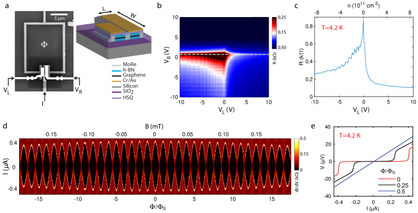
Figure 1a shows a scanning electron micrograph and cross-sectional schematic of a device. It consists of two encapsulated graphene JJs contacted with MoRe, incorporated in a SQUID loop. The fabrication strategy is similar to earlier work Calado et al. (2015) and further details are provided in the Supplementary Information (SI). The left (L-JJ)/right (R-JJ) JJs can be tuned independently by applying voltages (/) to local top gates. The junctions are intentionally designed to have a geometrical asymmetry, which ensures that the critical current of R-JJ () is larger than that of L-JJ () at the same carrier density. We report on two devices (Dev1 and Dev2) both of which have the same lithographic dimensions (L W) for L-JJ (400 nm 2 m). The dimensions of R-JJ for Dev1 and Dev2 are 400 nm 4 m and 400 nm 8 m respectively. All measurements were performed using a dc current bias applied across the SQUID, in a dilution refrigerator with a base temperature of 40 mK.
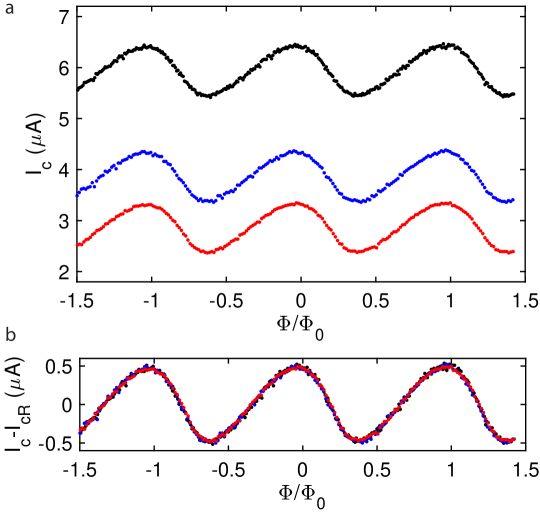
Figure 1b shows the variation in the normal state resistance () of the SQUID with and at K. The device was biased with a relatively large current of 500 nA, which is larger than the critical current of the SQUID for most of the gate range. Figure 1c shows a single trace taken along the white dashed line of Figure 1b, where R-JJ is held at the charge neutrality point (CNP). We see clear FP oscillations on the hole () doped region due to the formation of junctions at the superconductor-graphene interfaces Calado et al. (2015); Shalom et al. (2016). Furthermore, the criss-cross pattern seen in the lower left quadrant of Figure 1b indicates that both graphene junctions are in the ballistic limit and that there is no cross-talk between the individual gates. We note that when V the critical current of the SQUID () is larger than the applied current bias, and a zero-resistance state is thus visible even at 4.2 K. Having established the fact that our JJs are in the ballistic regime, we now look in more detail at the behavior of the SQUID. At K we first tune the gate voltages ( V, V) such that the SQUID is in a symmetric configuration and . Figure 1d shows the variation in differential resistance with current bias and magnetic field , where we observe clear oscillations in with magnetic flux. In this configuration, the modulation in is nearly 100 %, as seen by the individual traces in Figure 1e. The slow decay in the maximum value of arises due to the (Fraunhofer) magnetic field response of a single junction. The devices were designed such that this background was negligible around (i.e., the SQUID loop area was kept much larger than the JJ area). Minimizing this background is important for a reliable determination of the CPR, as we will see below.
We now turn our attention to the flux-dependent response of a highly asymmetric SQUID (), a condition which can be readily achieved by tuning the gate voltages appropriately. To outline the working principle of the device, we start with the assumption that both JJs have a sinusoidal CPR (a more general treatment can be found in the SI). So, the critical current of the SQUID can be written as , where () is the phase drop across L-JJ (R-JJ). When an external magnetic flux () threads through the SQUID loop, the flux and phase are related by , assuming the loop inductance is negligible. Now, when the phase difference across R-JJ is very close to . Thus, and the flux-dependence of directly represents the CPR of L-JJ, i.e., , where is the supercurrent through L-JJ and is the phase drop across it. This principle of using an asymmetric SQUID to probe the CPR has been employed in the past for systems such as point contacts Miyazaki et al. (2006); Della Rocca et al. (2007) and vertical graphene JJs Lee et al. (2015), where an SIS junction (with a well known sinusoidal CPR) was used as the reference junction. In our case, the reference junction is also a graphene JJ, where the CPR is not known a priori. We show (see SI) that this does not affect our ability to probe the CPR, provided time reversal symmetry is not broken, meaning that the CPR satisfies the condition Golubov et al. (2004). Throughout the remainder of the text we use R-JJ as the reference junction (larger critical current), and L-JJ is the junction under study (smaller critical current).
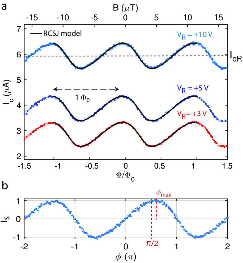
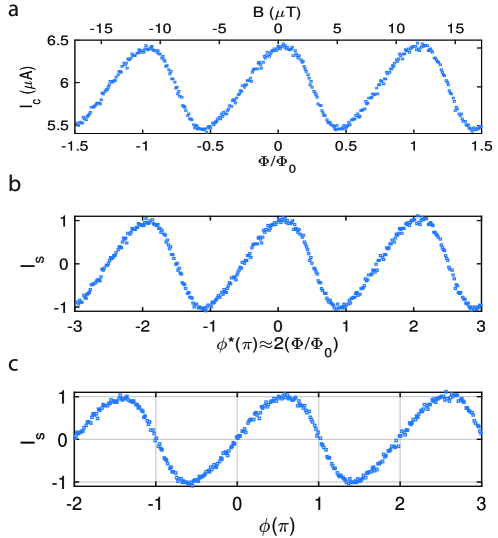
Figure 2a shows the typical magnetic response of the asymmetric SQUID at mK, with V (fixed) and different values of . For the most asymmetric configuration ( V) oscillates around a fixed value of roughly 6 A () with an amplitude of about 500 nA (). Using the arguments described above, this curve can be converted to , as shown in Figure 2b. Here is the normalized supercurrent defined as . We note that there is an uncertainty (less than one period) in the exact position of zero . This, combined with the unknown CPR of the reference graphene JJ, makes it important to do this conversion carefully, and we describe the details in the SI. The CPR shows a clear deviation from a sinusoidal form, showing a prominent forward skewing (i.e., peaks at ). We define the skewness of the CPR as English et al. (2016), where is the phase for which the supercurrent is maximum.
To be certain that we are indeed measuring the CPR of L-JJ, we perform some important checks. We keep fixed and reduce (by reducing ). Figure 2a shows that reducing merely shifts the downwards and therefore does not affect the extracted CPR, as one would expect. Furthermore, we use the experimentally determined CPR (from Figure 2b), the junction asymmetry, and loop inductance as inputs for the resistively and capacitively shunted junction (RCSJ) model to compute the expected SQUID response (see SI for details of the simulations). These plots (solid lines) show an excellent agreement between simulations and experiment, thus confirming that the asymmetry of our SQUID is sufficient to reliably estimate the CPR of L-JJ. Furthermore, it shows that there are no significant effects of inductance in our measurements, which could potentially complicate the extraction of the CPR from in an asymmetric SQUID Fulton et al. (1972).
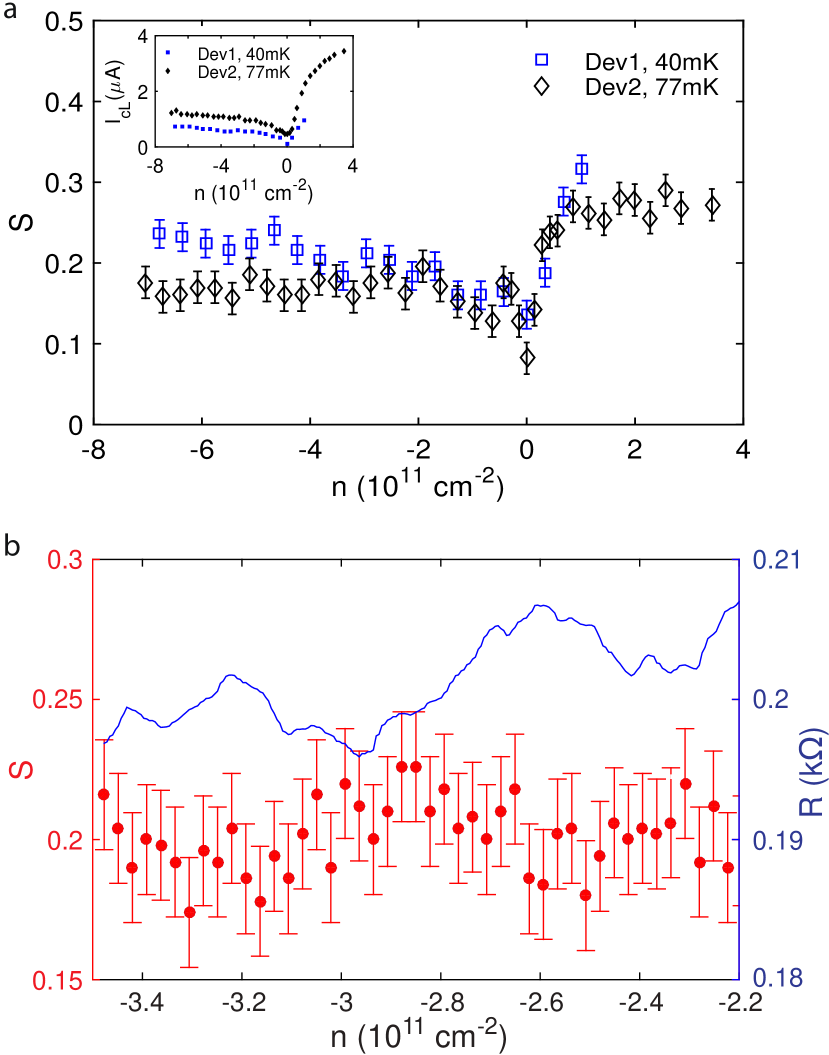
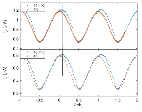
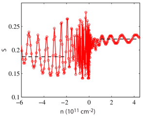
To study the gate dependence of the CPR we fix at +10 V (to maximize ) and study the change in with (Figure 3a) for Dev1 and Dev2. For both devices we find that is larger on the n-side as compared to the p-side, showing a dip close to the CNP. We note that Dev2 allows us to probe the CPR up to a larger range on the n-side due to its larger geometric asymmetry (see SI for other measurements on Dev2). We expect the skewness to depend strongly on the total transmission through the graphene JJ, which should depend on (a) the number of conducting channels in the graphene, as well as (b) the transparency of the graphene-superconductor interface. The gate voltage obviously changes the Fermi wave vector, but it also changes the contact resistance Wang et al. (2013), which plays a significant role in determining . This can be seen most clearly for Dev2 for high n-doping, where saturates, despite the fact that continues to increase up to the largest measured density (see inset). At large p-doping also seems to saturate, but a closer look (Figure 3b) shows that oscillates in anti-phase with the FP oscillations in resistance. This clearly indicates that in this regime the CPR is modulated by phase coherent interference effects similar to the FP oscillations which affect the total transmission.
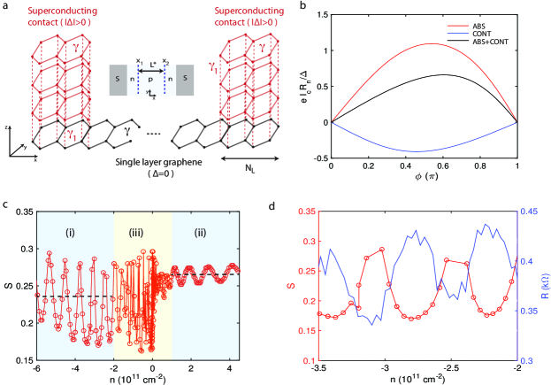
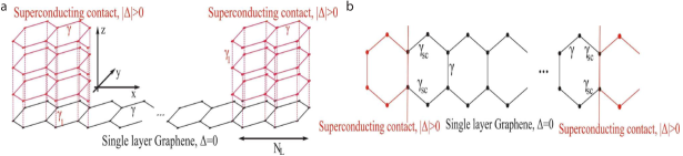
We complement our measurements with a minimal theoretical model by solving the corresponding Bogoliubov-de Gennes (BdG) equations to calculate the CPR in graphene JJs. To set the stage, we note that SNS junctions can be characterized by the quasiparticle mean free path in the normal (N) region and the coherence length , where is the Fermi velocity in N. In our devices , i.e., they are in the ballistic regime, and therefore we neglect impurity scattering in our calculations. Taking m/s for graphene and meV for MoRe, one finds nm, which means that in our junctions , i.e., they are not in the strict short junction limit . Consequently, the Josephson current is carried not only by discrete Andreev bound states (ABSs), but also by states in the continuum (CONT) Svidzinsky et al. (1973); Giuliano and Affleck (2013); Perfetto et al. (2009). To this end we numerically solve the BdG equations using a tight-binding (TB) model (see Figure 4a) and a recently developed numerical approach Rakyta et al. (2016); Equ which handles the ABSs and states in the continuum on equal footing. The description of both the normal region and the superconducting terminals is based on the nearest-neighbor TB model of graphene Wakabayashi et al. (1999). The on-site complex pair-potential is finite only in the superconducting terminals and changes as a step-function at the N-S interface. The results presented here are calculated using the top-contact geometry (Figure 4a), a model with perfect edge contacts is discussed in the SI. As observed experimentally, we take into account -doping from the superconducting contacts (see Figure 4b). If the junction is gated into hole-doping, a FP cavity is formed by the two junctions in the vicinity of the left and right superconducting terminals. The length of this FP cavity depends on the gate voltage Shalom et al. (2016), for stronger hole-doping the n-p junctions shift closer to the contacts. For further details of the model see SI.
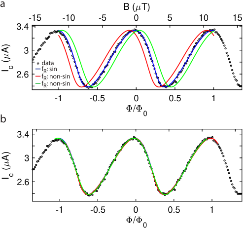
Turning now to the CPR calculations, Figure 4b shows separately the contribution of the ABS and the continuum to the supercurrent. Since , the latter contribution is not negligible and affects both the value of the critical current and the skewness of the CPR. In Figure 4c we show the calculated skewness as a function of the doping of the junction at zero temperature. We consider three regimes: (i) strongly -doped junction; (ii) large -doping, (iii) the region around the CNP. We start with the discussion of (i). It is well established that in this case the - junctions lead to FP oscillations in the normal resistance as well as in the critical current Calado et al. (2015); Shalom et al. (2016) of graphene JJs. Our calculations, shown in Figure 4d, indicate that due to FP interference the skewness also displays oscillations as a function of doping around an average value of . As already mentioned, similar oscillations are present in the normal state resistance , however, we find that oscillates in antiphase with the skewness. Compared to the measurements (Figure 3b), our calculations therefore reproduce the phase relation between the oscillations of the skewness and and give a qualitatively good agreement with the measured values of the skewness. In the strong -doped regime (case ii) the calculated average skewness of is larger than for -doped junctions, and very close to the measured values. Small oscillations of are still present in our results and they are due to the - interfaces, i.e., the difference in the doping close to the contacts (for and ) in Figure 4a and the junction region (), which enhances backscattering. Our calculations therefore predict smaller skewness for -doped than for -doped junctions. The enhancement of in the -doped regime can be clearly seen in the measurements of Figure 3a. We note that previous theoretical work Black-Schaffer and Linder (2010), which calculated the spatial dependence of the pairing amplitude self-consistently, predicted a skewness of for -doped samples with , while a non-self-consistent calculation which took into account only the contribution of the ABS yielded Black-Schaffer and Linder (2010). The comparison of these results to ours, and to the measurements, suggest that the skewness may depend quite sensitively on the S-N interface as well as on the ratio and that our approach captures the most important effects in these junctions. Finally, we briefly discuss the case (iii), where the measurements show a suppression of the skewness as the CNP is approached. The measured values of are similar to those found in diffusive junctions English et al. (2016), but significantly lower than the theoretical prediction of in the short junction limit Titov and Beenakker (2006) at the CNP. This suppression of is not reproduced in our calculations, instead, we find rapid oscillations as the CNP is approached from the -doped regime. This discrepancy is likely to be due to effects that are not included in our ballistic model, such as charged scatterers which are poorly screened in this regime, or scattering at the edges, which is more relevant at low densities when only a few open channels are present.
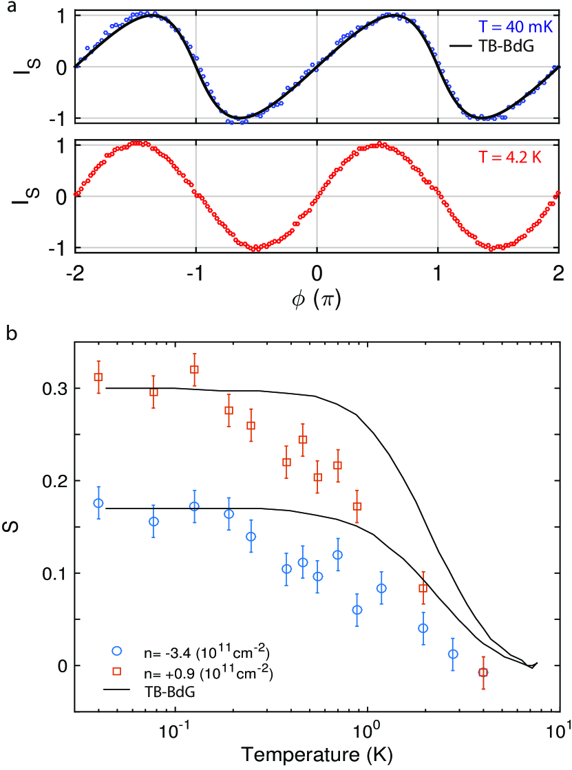
Finally, we study the effect of temperature on the CPR of these JJs. In Figure 5a, we compare the CPR in the n-doped regime ( V; cm-2) at 40 mK and 4.2 K. One clearly sees that at 4.2 K the CPR is sinusoidal. This is consistent with our observation that the critical current modulation of the SQUID is nearly 100 % at 4.2 K (Figure 1d), a condition which can only be achieved if the CPR is sinusoidal. Figure 5b shows the full temperature dependence of for two representative values of electron and hole doping. The reduction in skewness with temperature is a consequence of the fact that the higher frequency terms in the CPR arise due to the phase coherent transfer of multiple Cooper pairs and involve longer quasiparticle paths Heikkilä et al. (2002), thereby making them more sensitive to temperature. As a result, their amplitude decreases quickly with increasing temperature Hagymási et al. (2010); Black-Schaffer and Linder (2010); Rakyta et al. (2016); English et al. (2016). Numerical estimates show the same qualitative behavior, however the experimentally determined skewness reaches zero (sinusoidal CPR) faster than the numerics. At this point it is difficult to ascertain the exact reason for this discrepancy, but one possible explanation for this is that the induced superconducting gap in the graphene is somewhat smaller than the bulk MoRe gap, resulting in a faster decay.
In conclusion, we have used a fully gate-tunable graphene based SQUID to provide measurements of the current-phase relation in ballistic Josephson junctions made with encapsulated graphene. We show that the CPR is non-sinusoidal and can be controlled by a gate voltage. We complement our experiments with tight binding simulations to show that the nature of the superconductor-graphene interface plays an important role in determining the CPR. We believe that the simplicity of our device architecture and measurement scheme should make it possible to use such devices for studies of the CPR in topologically non-trivial graphene Josephson junctions.
Acknowledgements: We thanks A. Geresdi and D. van Woerkom for useful discussion. S.G. and L.M.K.V acknowledge support from the EC-FET Graphene flagship and the Dutch Science Foundation NWO/FOM. A.K. acknowledges funding from FLAG-ERA through project ’iSpinText’. P.R. acknowledges the support of the OTKA through the grant K108676, the support of the postdoctoral research program 2015 and the support of the János Bolyai Research Scholarship of the Hungarian Academy of Sciences. K.W. and T.T. acknowledge support from the Elemental Strategy Initiative conducted by the MEXT, Japan and JSPS KAKENHI Grant Numbers JP26248061,JP15K21722 and JP25106006.
References
- Efetov et al. (2016) D. K. Efetov, L. Wang, C. Handschin, K. B. Efetov, J. Shuang, R. Cava, T. Taniguchi, K. Watanabe, J. Hone, C. R. Dean, and P. Kim, Nature Physics 12, 328 (2016).
- Lee et al. (2016) G. H. Lee, K. F. Huang, D. K. Efetov, D. S. Wei, S. Hart, T. Taniguchi, K. Watanabe, A. Yacoby, and P. Kim, arXiv:1609.08104 (2016).
- Calado et al. (2015) V. E. Calado, S. Goswami, G. Nanda, M. Diez, A. R. Akhmerov, K. Watanabe, T. M. K. T. Taniguchi, and L. M. K. Vandersypen, Nature Nanotechnology 10, 761 (2015).
- Shalom et al. (2016) M. B. Shalom, M. J. Zhu, V. I. Fal’ko, A. Mishchenko, A. V. Kretinin, K. S. Novoselov, C. R. Woods, K. Watanabe, T. Taniguchi, A. K. Geim, and J. R. Prance, Nature Physics 12, 318 (2016).
- Allen et al. (2016) M. T. Allen, O. Shtanko, I. C. Fulga, A. R. Akhmerov, K. Watanabe, T. Taniguchi, P. Jarillo-Herrero, L. S. Levitov, and A. Yacoby, Nature Physics 12, 128 (2016).
- Amet et al. (2016) F. Amet, C. T. Ke, I. V. Borzenets, J. Wang, K. Watanabe, T. Taniguchi, R. S. Deacon, M. Yamamoto, Y. Bomze, S. Tarucha, and G. Finkelstein, Science 352, 966 (2016).
- Borzenets et al. (2016) I. V. Borzenets, F. Amet, C. T. Ke, A. W. Draelos, M. T. Wei, A. Seredinski, K. Watanabe, T. Taniguchi, Y. Bomze, M. Yamamoto, S. Tarucha, and G. Finkelstein, Phys. Rev. Lett. 117, 237002 (2016).
- Murani et al. (2016) A. Murani, A. Kasumov, S. Sengupta, Y. Kasumov, V.T.Volkov, I. Khodos, F. Brisset, R. Delagrange, A. Chepelianskii, R. Deblock, H. Bouchiat, and S. Guéron, arXiv:1609.04848 (2016).
- Miyazaki et al. (2006) H. Miyazaki, A. Kanda, and Y. Ootuka, Physica C 437, 217 (2006).
- Della Rocca et al. (2007) M. L. Della Rocca, M. Chauvin, B. Huard, H. Pothier, D. Esteve, and C. Urbina, Phys. Rev. Lett. 99, 127005 (2007).
- Wiedenmann et al. (2016) J. Wiedenmann, E. Bocquillon, R. S. Deacon, S. Hartinger, O. Herrmann, T. M. Klapwijk, L. Maier, C. Ames, C. Brüne, C. Gould, A. Oiwa, K. Ishibashi, S. Tarucha, H. Buhmann, and L. W. Molenkamp, Nature Communications 7, 10303 (2016).
- Titov and Beenakker (2006) M. Titov and C. W. J. Beenakker, Phys. Rev. B 74, 041401 (2006).
- Hagymási et al. (2010) I. Hagymási, A. Kormányos, and J. Cserti, Phys. Rev. B 82, 134516 (2010).
- Black-Schaffer and Doniach (2008) A. M. Black-Schaffer and S. Doniach, Phys. Rev. B 78, 024504 (2008).
- Black-Schaffer and Linder (2010) A. M. Black-Schaffer and J. Linder, Phys. Rev. B 82, 184522 (2010).
- Rakyta et al. (2016) P. Rakyta, A. Kormányos, and J. Cserti, Phys. Rev. B 93, 224510 (2016).
- San-Jose et al. (2015) P. San-Jose, J. Lado, R. Aguado, F. Guinea, and J. Fernández-Rossier, Phys. Rev. X 5, 041042 (2015).
- English et al. (2016) C. D. English, D. R. Hamilton, C. Chialvo, I. C. Moraru, N. Mason, and D. J. Van Harlingen, Phys. Rev. B 94, 115435 (2016).
- Lee et al. (2015) G. H. Lee, S. Kim, S. H. Jhi, and H. J. Lee, Nature Communications 6, 6181 (2015).
- Girit et al. (2008) Ç. Girit, V. Bouchiat, O. Naaman, Y. Zhang, M. F. Crommie, A. Zettl, and I. Siddiqi, Nano Letters 9, 198 (2008).
- Girit et al. (2009) Ç. Girit, V. Bouchiat, O. Naaman, Y. Zhang, M. F. Crommie, A. Zettl, and I. Siddiqi, Phys. Status Solidi B 246, 2568 (2009).
- Golubov et al. (2004) A. A. Golubov, M. Y. Kupriyanov, and E. Il’ichev, Rev. Mod. Phys. 76, 411 (2004).
- Fulton et al. (1972) T. A. Fulton, L. N. Dunkleberger, and R. C. Dynes, Phys. Rev. B 6, 855 (1972).
- Wang et al. (2013) L. Wang, I. Meric, P. Y. Huang, Q. Gao, Y. Gao, H. Tran, T. Taniguchi, K. Watanabe, L. M. Campos, D. A. Muller, J. Guo, P. Kim, J. Hone, K. L. Shepard, and C. R. Dean, Science 342, 614 (2013).
- Svidzinsky et al. (1973) A. V. Svidzinsky, T. N. Antsygina, and E. N. Bratus, J. Low Temp. Phys. 10, 131 (1973).
- Giuliano and Affleck (2013) D. Giuliano and I. Affleck, J. Stat. Mech. , P02034 (2013).
- Perfetto et al. (2009) E. Perfetto, G. Stefanucci, and M. Cini, Phys. Rev. B 80, 205408 (2009).
- (28) The numerical calculations were performed with the EQuUs software, see http://eqt.elte.hu/equus/home.
- Wakabayashi et al. (1999) K. Wakabayashi, M. Fujita, H. Ajiki, and M. Sigrist, Phys. Rev. B 59, 8271 (1999).
- Heikkilä et al. (2002) T. T. Heikkilä, J. Särkkä, and F. K. Wilhelm, Phys. Rev. B 66, 184513 (2002).
I Supplementary Information
II 1. Device Fabrication
Graphene flakes are exfoliated onto silicon chips with 90 nm SiO2. Next, h-BN is exfoliated separately on a glass slide covered by a 1-cm2 piece of PDMS coated with an MMA/MAA copolymer layer. This glass slide is baked for 20 minutes on a hot plate at , prior to h-BN exfoliation. The glass slide is mounted on a micromanipulatior in a home-built set-up (similar to Ref Steele_s ) equipped with a heating stage. Next, a h-BN flake on the slide is aligned with the target graphene and the substrate is heated to C. The flakes are brought into contact, after which the glass slide is released smoothly such that the graphene flake is picked up by the h-BN flake on the glass slide. Finally, the graphene/h-BN stack is transferred onto another h-BN flake (exfoliated onto a silicon chip with 285 nm SiO2), at a temperature of C.
The processing flow is outlined in Figure S1. First MoRe contacts are made to the stack via an etch fill technique Calado_s using standard e-beam lithography. The sample is plasma-etched for 1 min in a flow of 40/4 sccm CHF3/O2 with 60 W power, and bar pressure. After etching, we immediately sputter 70 nm MoRe using a DC plasma with a power of 100 W in an Argon atmosphere. Next, the MoRe lift-off is completed in hot () acetone for about 3-4 hours. The two JJs are shaped using another e-beam lithography in which the intended graphene geometry is defined via a PMMA/hydrogen-silsesquioxane (HSQ) mask, followed by CHF3/O2 etching. In order to isolate the contacts from the top gate, we use 170 nm of HSQ as a dielectric. Finally, top gates are fabricated by e-beam evaporation of 5nm Cr + 120 nm Au, and subsequent lift off in hot acetone.
III 2. Ballistic transport in Dev2
IV 3. Magnetic field to phase conversion
In the main text we pointed out that one must take care in converting the flux-periodic oscillations of the critical current of the SQUID to the CPR of L-JJ . Figure S3 shows how this is done. We start with the upper plot in Figure 2a of the main text, which is shown here again for convenience (Figure S3a). We then subtract a constant background () about which the curve oscillates and normalize it with respect to the oscillation amplitude (). Also, the flux is converted to phase by . This is not the true phase for two important reasons. Firstly, the zero of the magnetic field is not known precisely. Secondly, the flux to phase conversion is only possible up to a constant offset, which is determined by the CPR of R-JJ (which is a-priori unknown). In order obtain the CPR we then offset the curve in Figure S3b along the axis such that the supercurrent at zero phase difference is zero, which finally gives us the CPR. We note that this procedure is only valid for systems where and , both of which are reasonable assumptions for our graphene JJs.
V 4. Eliminating inductance effects
In an asymmetric SQUID inductance effects can give rise to skewed curves. It is therefore important to establish that such effects do not dominate the response of the SQUIDs described in this study. To do so, we first provide some qualitative arguments which make it evident that the skewness arises only from a non-sinusoidal CPR. Furthermore, we extract the loop inductance of our SQUID, use it as an input for the RCSJ model and confirm that (within our experimental resolution) the inductance does not play an important role in determining the shape of the curves, and hence does not affect our ability to measure the CPR.
V.1 Large asymmetry
We have shown that for large asymmetry (i.e., ), we probe the CPR of L-JJ. We define the asymmetry parameter . Figure S4a shows three traces at mK, where A is kept fixed and is varied from 6 A (black trace, ) to 2.8 A (red trace, ). Figure S4b shows that all three curves collapse despite the fact that the maximum critical current () changes by a factor of two. If the skewness was dominated by inductance effects, we would have not expected this collapse, since the screening parameter increase by a factor of two (going from the red trace to the blue trace). In other words, the combined effect of large asymmetry and inductance should have resulted in a larger skewing of the black trace (maximum and ) as compared to the red one.
V.2 Intermediate asymmetry
We have shown in the main text (Figure 5) that the skewness of the CPR decreases with increasing temperature, resulting in a sinusoidal CPR at 4.2 K. One might argue that this is consistent with inductance effects, whereby an increase in temperature reduces the critical currents and hence . To eliminate this possibility, we compare at 40 mK and 4.2 K. Figure S5a,b show two such data sets. In each case the gate voltages were tuned such that both and were roughly the same for both temperatures. We see that at 40 mK the curves are noticeably skewed as compared to 4.2 K. The asymmetry here is not sufficient to directly extract the CPR, but it clearly demonstrates that the non-sinusoidal CPR also manifests itself in skewed curves at intermediate asymmetry. We note that this argument is made stronger by the fact that the inductance at 4.2 K should in fact be larger than that at 40 mK, since the inductance of the MoRe loop is dominated by kinetic inductance, which increases at higher temperatures. In other words, one would expect inductance related effects to be enhanced at higher temperatures, rather than become suppressed.
V.3 Estimating the loop inductance
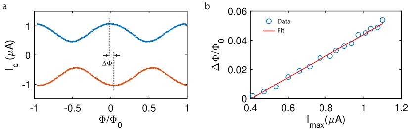
Figure S6a shows measurements of an asymmetric SQUID at 4.2 K, where we have established that the CPR is sinusoidal. The position of maximum for positive and negative current bias are offset along the flux axis due to self-flux effects Goswami_s . This shift is given by: , where and are the critical current of right and left junction respectively. Figure S6b shows the variation of with . These values are obtained by keeping A fixed and varying from 0.2 A (symmetric configuration) to 0.9 A (highly asymmetric). Since , a linear fit (red line) allow us to extract pH. Since MoRe is a highly disordered superconductor, its inductance is dominated by the kinetic inductance and the low temperature inductance , giving pH at mK. We use this inductance to compare our experiments with the RCSJ simulations described below.
VI 5. RCSJ Model
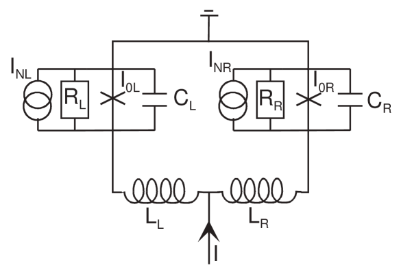
To model the asymmetric SQUID we consider the circuit shown in Figure S7. The Josephson junctions are described by the resistively and capacitively shunted junction (RCSJ) modelMcCumber_s ; Stewart_s by Josephson currents with phases and and amplitudes and , resistors and , and capacitors and . The Josephson currents are given by and , where are the normalized current-phase relations of the left and right JJ, respectively. The Nyquist noise arising from the two resistors is described by two independent current noise sources and having white spectral power densities 4 and 4, respectively. The two arms of the SQUID loop have inductances and . The total inductance is the sum of the geometric (Lg) and the kinetic (Lk) inductance. The loop is biased with a current , and a flux is applied to the loop.
In the following we are interested only in static solutions and normalize currents by . The currents and through the left (right) arm of the SQUID are then given by:
| (1) |
| (2) |
Assuming for simplicity that (a reasonable assumption based on our device geometry) the normalized circulating current j is given by:
| (3) |
and the maximum current across the SQUID is . From Equation 3 we obtain
| (4) |
Let us consider the case , i.e., the right junction has a much larger critical current than the left one. As we will see, in this case the modulation of the SQUID critical current reflects the CPR of the left junction, provided that .
| (5) |
From Equation 4, for , we obtain . Thus
| (6) |
Let us assume that . Then the task is to maximize with respect to , to obtain ic,SQUID vs . If the critical current of the right JJ is much bigger than the critical current of the left JJ, the value of will be close to the value where the CPR of the right JJ has its maximum. We thus Taylor expand:
| (7) |
Note that in Equation 7 the first derivative of is zero, because we look for the maximum of this CPR. If the second derivative is reasonably peaked, will be very close to and we obtain:
| (8) |
This means that ic,SQUID vs. probes the CPR of the left JJ up to a phase shift . can be evaluated further if one assumes that at and that min() = - max().
In Figure 2a of the main text we have compared our experiments with a full RCSJ simulation, as described above. These simulations involve no free parameters since we use the experimentally determined inductance, asymmetry (), and CPR of L-JJ as input parameters. For simplicity, the numerical plots were generated assuming a sinusoidal CPR for the reference junction R-JJ, shown as the blue curve in the Figure S8a. The red curve shows how changes when R-JJ is assumed to have a non-sinusoidal CPR (with a functional form similar to that extracted for L-JJ). The only effect this has is to offset the simulated curves along the flux axis. This is a consequence of the fact that (as described above) is different for the two cases. However, we see in Figure S8b that these two cases perfectly overlap with an appropriate offset along the flux axis. This confirms the fact that an incomplete knowledge of the CPR of R-JJ is (in practice) equivalent to an unknown offset in magnetic field, and therefore does not affect our ability to accurately determine the functional form of the CPR of L-JJ. The green curve in Figure S8a is a simulation with (i.e., in the limit where the loop inductance is negligible). Looking carefully at Figure S8b shows that this has a slightly different shape as compared to the blue/red curves. However, this difference is well within the error bars for our estimation of the skewness, and we can conclude that the functional form of the curves is not dominated by the inductance effects, but by the non-sinusoidal CPR of L-JJ. This is in agreement with the conclusions drawn from more qualitative arguments presented in the previous section.
VII 6. Tight Binding-Bogoliubov-de Gennes Calculations
VII.1 Details of the theoretical model
In this Section we provide further details of the theoretical model that we used in our numerical calculations. As it will be clear from the following discussion, we found that in order to obtain a good qualitative agreement with the measurements, a realistic and detailed model of the Josephson junction, especially the interface between the superconductor and the normal regions, is needed.
We assume that the graphene flake which serves as a weak link is perfectly ballistic and scattering processes only occur at the interfaces between regions of different doping in the normal part of the junction or between the superconductor and the normal region. The normal (N) and superconducting (S) regions are of the same width in our calculations. This allows us to use periodic boundary conditions perpendicular to the transport direction. The transverse momentum is a good quantum number and the DC Josephson current can be calculated as a sum over all :
| (9) |
where is the momentum resolved Josephson current calculated for a specific transverse momentum via the contour integral method developed recently in Reference method_s . For wide junctions and high dopings, when there are many transverse momenta, the exact form of the boundary conditions is not important and therefore we used the infinite mass boundary condition to obtain : where and is the width of the junction.
The description of both the N region and the S terminals is based on the nearest-neighbour tight-binding model of graphenegraphene-TB_s
| (10) |
where is the on-site energy on the atomic site , eV is the hopping amplitude between the nearest-neighbor atomic sites in the graphene lattice, and ( ) is a creation (annihilation) operator for electrons at site . We considered two junction geometries. Most of our results were obtained using the top-contact geometry, which is shown in Figure 4(a) of the main text and for convenience repeated here in Figure S9(a). The S terminals are described by vertically stacked graphene layers (AA stacking) where the inter-layer hopping is given by eV. The same inter-layer hopping was also used between the S terminals and the N region. The S leads are coupled to the normal graphene sheet over unit cells. The result do not depend strongly on the exact value of , therefore we used in our calculations.
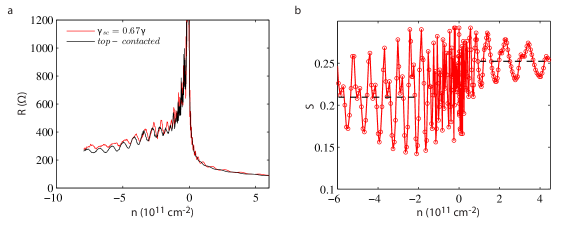
To mimic metallic leads with many open channels, the S terminals are highly -doped. This is described by an on-site potential and we used meV in our calculations. For high -doping of the N region we calculated an average transparency of for the junction, see the Supplementary of Reference Falko_s for the precise definition of . We find that the calculated does not depend very sensitively on the precise value and because most of the backscattering taking place at the interface of the S leads and the N region is due to a “geometric” effect: the electron trajectories have to turn at right angle to arrive from the lead into the N region. Moreover, we find that for the calculated dependence of the normal state resistance on the doping of the N region agrees qualitatively well with the measurements where the right JJ was kept at the charge neutrality point [c.f. Figure 1(c) in the main text and Figure S12(a) below]. (We did not try to achieve quantitative agreement for because in the experiments the resistance of the two junctions are always measured in parallel, whereas we used single junctions in the calculations.)
As shown in Figure S9(b) and discussed further later on, we have also made calculations using the side-contact geometry. For both geometries we used open boundary conditions for the leads in the transport direction (which is the direction in top-contacted geometry and the direction in the side-contacted one, see Figure S9).
In contrast to the S leads, which are always n-doped in our calculations, the normal region of the JJ can be either or doped depending on the gate voltage. This is modeled by a doping potential . Experimentally, it was shown that the superconducting terminals -dope the normal region of the JJ Calado_s ; Falko_s . This -doped region extends to a distance () from the left (right) terminal, where is the distance between the two S leads. The potential profile in the junction can be therefore either or . The exact value of the and , and hence the cavity length , however, depends on the gating of the JJ. In the regime, where clear FP oscillations can be measured in the normal state resistance in our devices, we extracted the experimental cavity length using the relation , where is the density difference between consecutive peaks in rickhaus_s .
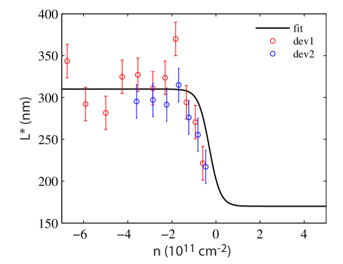
The results of this analysis are summarized in Figure S10. We find that nm is roughly constant for , but it decreases for densities approaching the CNP. In order to extract the theoretical cavity length for , we fitted the experimental results by the function
| (11) |
Here is the cavity length for strongly doped junctions which could not be determined from the measurements, therefore we used nm. As mentioned above, a good qualitative agreement between the calulated and measured normal state resistance is achieved using this value of . We have also checked that for nm the calculation results do not depend strongly on the exact value of . The two fitting parameters in Eq. (11) are and and we found and , see Figure S10. Once is determined, the parameters and are given by and . The total potential profile along the junction, which describes the smooth transition between the highly doped regions ( and ) and the central part of the junction () is modeled by
| (12) |
where the parameter controls the smoothness of the transition. We used in our calculations corresponding to a relatively sharp transition. Larger values of would effectively mean that the leads dope the N region of the junction and the doping there would therefore not be determined by .
Finally, superconductivity in the S terminals is modelled by a on-site, complex pair-potential which goes to zero as a step-function at the S-N interface. We made sure that that the Fermi-wavelengths and in the N and S regions, respectively, satisfy . This ensures that the exact spatial dependence of the superconducting pair potential at the N-S interface is not very important in the calculationsbeenakker-sgs_s .
VII.2 Soft vs hard superconducting gap
Following Reference soft_gap_s , we also considered the effect of quasiparticle broadening in the superconducting terminals by introducing a complex energy shift in the self-energy calculations. Such a broadening, described by the parameter , can arise due to scattering with phonons or other electrons or due to other effects leading to quasiparticle poisoning.
We find that a finite can considerably affect the value of the calculated critical current . Since is not the main focus of this work, we do not discuss the details here. Instead, we present results to illustrate the effect of on the skewness. We repeated the calculations using and the results are shown in Figure S11. Comparing Figure 4(d) in the main text and Figure S11, one can notice that the results are qualitatively very similar, but for the average skewness is larger for both and doping than for . We note that in the regime the calculated average skewness for is closer to the measured one than the result for . The opposite is true in the regime, where the calculations with () yielding () give better agreement with the measurements (). We were not able to achieve an equally good agreement in both the and regimes using a single value of . This may indicate that depends on the doping of the junction, but one would need a more microscopic understanding of the processes that contribute to .
We emphasize, however, that is not the only parameter which can affect the value of the skewness. Generally, the value of the skewness depends on the interface between the S and N regions. Calculations not shown here indicated that the presence/absence of a smooth transition between the highly doped leads and the normal graphene region (the parameter in Eq.12) and the value of the hopping amplitude in Figure S9(b) between the S and N regions can also affect the results. However, we fixed the value of the parameters describing the junction such that we obtain a qualitatively good agreement for (as discussed previously) and did not changed these parameters in the skewness calculations.
VII.3 Calculations using the side contact geometry
We also performed calculations using the side-contact geometry, which is shown in Figure S9(b). This contact geometry has recently been employed, e.g., in Reference bouchiat_s to model diffusive graphene JJs both in the short and in the long junction regime. The most important results of our calculations are shown in Figure S12. We have used the same doping profile along the junction as in the top-contact geometry. As it can be seen in Figure S12(a), by choosing , the doping dependence of the normal state resistance is qualitatively very similar for both models. One can notice, however, that the amplitude of the oscillations for doping is larger in the side-contact geometry. In the regime the amplitude of the FP oscillations is somewhat different, but the oscillations are in the same phase, except for large doping.
The skewness calculation for the side contact geometry is shown in Figure S12(b). We used the same and as for the corresponding calculation in the top-contact geometry. The result are qualitatively similar to those shown in Figure S11 and Figure 4(c) of the main text. In particular, the average skewness is different in the and doping regime, but the obtained values are larger than the ones calculated in the top-contact geometry for . However, the amplitude of the skewness oscillations is larger in the side-contact geometry, especially for doping, where they are three times larger than in Figure 4(c) of the main text. Such large oscillations are not present in the experimental data and for this reason we find a better overall agreement between the experiments the the calculations using the top-contact geometry. Finally, we briefly note in the vicinity of the CNP one can see large oscillations in the skewness and therefore both models fail to reproduce the experimental results in this regime.
References
- (1) A. Castellanos-Gomez, M. Buscema, R. Molenaar, V. Singh, L. Janssen, H. S. J. van der Zant, G. A. Steele, 2D Materials 1, 011002 (2014).
- (2) V. E. Calado, S. Goswami, G. Nanda, M. Diez, A. R. Akhmerov, K. Watanabe, T. Taniguchi, T. M. Klapwijk, L. M. K. Vandersypen, Nature Nanotechnology 10, 761 (2015).
- (3) S. Goswami, E. Mulazimoglu, A. M. R. V. L. Monteiro, R. Wölbing, D. Koelle, R. Kleiner, Ya. M. Blanter, L. M. K. Vandersypen, A. D. Caviglia, Nature Nanotechnology 11, 861 (2016).
- (4) W. C. Stewart, Appl. Phys. Lett. 12, 277 (1968).
- (5) D. E. McCumber, J. Appl. Phys. 39, 3113 (1968).
- (6) P. Rakyta, A. Kormányos, J. Cserti, Phys. Rev. B 93, 224510 (2016).
- (7) K. Wakabayashi, M. Fujita, H. Ajiki, and M. Sigrist, Phys. Rev. B 59, 8271 (1999).
- (8) M. Ben Shalom, M. J. Zhu, V. I. Fal’ko, A. Mishchenko, A. V. Kretinin, K. S. Novoselov, C. R. Woods, K. Watanabe, T. Taniguchi, A. K. Geim and J. R. Prance, Nature Physics 12, 318 (2016).
- (9) P. Rickhaus, R. Maurand, M-H. Liu, M. Weiss, K. Richter, and C. Schönenberger, Nature Communications 4, 2342 (2013).
- (10) M. Titov and C. W. J. Beenakker, Phys. Rev. B 74, 041401 (2006).
- (11) S. Takei, B. M. Fregoso, H. Y. Hui, A. M. Lobos, and S. Das Sarma, Phys. Rev. Lett. 110, 186803 (2013).
- (12) C. Li, S. Guéron, A. Chepelianskii, and H. Bouchiat, Phys. Rev. B 94, 115405 (2016).